A 674 nm External Cavity Diode
Laser for a
8 8
Sr+ Ion Trap
by
Susanna M. Thon
Submitted to the Department of Physics
in partial fulfillment of the requirements for the degree of
Bachelor of Science in Physics
- - l
ab bile
MASSACHUSETTS INSTITUTE OF TECHNOLOGY
June 2005
(2> .RQ n n \/ Th, a \/rTIlT All rirrbhQ rocorrlJ
w~k LL0b1-111uU V1L. -l "ki l- IVL.VlV . L lIl FllO L -)-1V -.
The author hereby grants to MIT permission to reproduce and
distribute publicly paper and electronic copies of this thesis document
in whole or in part.
/-.~/
Author
.
.
.
...
...
Dep] tment of Physics
[) l May 12, 2005
Certified
by ..,
...
...
Isaac. Chuang
Associate Professor
Thesis Supervisor
Accepted
by ...
..-...
David Pritchard
Thesis Coordinator
ARCHIVES MASSACHUSETTS INSTIUE OF TECHNOLOGY JUN 0 7 2005 LIBRARIES IA 674 nm External Cavity Diode
Laser for a
88Sr+ Ion Trap
by
Susanna M. Thon
Submitted to the Department of Physics
on May 12, 2005, in partial fulfillment of the requirements for the degree of
Bachelor of Science in Physics
Abstract
Atomic ion traps are a promising candidate for scalable quantum information pro-cessing. In this thesis, a 674 nm extended cavity diode laser is built to address an optical quantum bit in 88Sr+ with the goal of testing such traps. To find this transi-tion, a depletion experiment is performed in which the 674 nm transition depopulates the principal 422 nm transition, causing a dip in the ion fluorescence signal. Our preliminary results suggest that this depletion signal has been observed.
Thesis Supervisor: Isaac L. Chuang
Acknowledgments
I gratefully thank Professor Isaac Chuang for his guidance and for teaching and
in-spiring me to be an experimentalist. Many thanks go to Ken Brown for his constant
patience, proofreading, and advice and for making my undergraduate research
expe-rience meaningful.
I would like to thank Rob Clark who is always helpful and entertaining. I also thank Jarek Labaziewicz for fixing everything that broke and for telling me to go
home at 2 a.m.
Finally, I would like to thank the rest of the members of the Quanta group for their advice and support.
Contents
1 Introduction
1.1 M otivation . . . . 1.2 O verview . . . .
1.3 Contributions to This Work ...
2 Background
2.1 Atomic Ion Trapping ... 2.2 The Strontium Ion ...
2.2.1 `SSr+ Energy Levels . . . . .
2.2.2 Uses of the 674 nm Line . . .
2.2.3 Specifics of the 674 nm Line .
2.3 External Cavity Diode Lasers .... 2.3.1 Laser Theory and Properties .
2.3.2 Diode Lasers ...
2.3.3 External Cavity Diode Lasers
3 Construction of the Laser Apparatus
3.1 Selection of the Laser Diode ....
3.2 The Diode Laser Box ...
3.3 Laser Performance ...
3.4 The Temperature Controller .... 3.5 Optical Breadboard Layout ....
11 11 12 13 15 15 17 17 18 21 21 21 24 26 29 29 30 31 32 34
...
...
...
...
...
...
...
...
...
...
...
...
...
...
4 Tuning the Laser 37
4.1 Temperature Dependence ... 37
4.2 Tuning with the Grating ... 39
4.3 Piezo Tuning ... 41
4.4 The Fabry-Perot Resonator . . . 42
5 The Depletion Experiment 45 5.1 Theoretical Predictions ... 45
5.2 Experimental Method ... 47
5.3 Data and Results ... 48
6 Conclusion 53
List of Figures
2-1 Electrode configuration in a linear Paul trap . . ... 16
2-2 Photograph of the electron gun and oven used in the ytterbium ion trap. 17 2-3 Image of a trapped strontium ion crystal produced by the CCD camera. 18 2-4 Energy level diagram for the 88Sr+ ion ... 19
2-5 Three and four energy level systems for producing population inversion. 22 2-6 Experimental set-up of a generic laser ... . 23
2-7 Illustration of a diffraction limited beam ... 24
2-8 Diagram of a laser diode package ... 25
2-9 A laser diode made from a p-n junction ... ... . 26
2-10 Diagram of the components involved in an external cavity diode laser. 27 2-11 The ECDL mode structures that determine the single mode laser wave-length ... 28
3-1 The laser diode package ... 30
3-2 Diagram of the laser box layout . . ... 31
3-3 Photograph of the inside of the laser box . . ... 32
3-4 Power output vs. injection current at 10.8°C, 20°C, and 30°C. .. 33
3-5 Photograph of the temperature controller ... 34
3-6 Graph of the set temperature and actual temperature vs. time .... 35
3-7 Photograph of the optical breadboard ... 36
4-1 Temperature dependence of the threshold lasing current . . ... 38
4-3 Diffraction grating used in the external cavity to tune the laser
wave-length ... 39
4-4 Diagram of the grating, lens, incident beam, and reflected beams. . . 40
4-5 Graph of the diffraction grating tuning profile . ... 41
4-6 Graph of laser wavelength vs. piezo voltage ... 42
4-7 A Fabry-Perot cavity consisting of two mirrors ... 43
4-8 Photograph of the Fabry-Perot resonator ... 44
4-9 Frequency and Fabry-Perot signal vs. piezo voltage . ... 44
5-1 Example of the first type of depletion experiment scan ... 48
5-2 Example of the second type of depletion experiment scan . ... 49
Chapter 1
Introduction
1.1 Motivation
Atomic ion traps are a promising architecture for quantum information processing. The basic requirements for quantum computing, which are quantum state
prepara-tion, manipulaprepara-tion, and read-out, have all been achieved in ion trap systems. [KMW02]
In order to achieve the goal of building a quantum computer out of atomic ion traps, it is necessary to test trap designs. The project described in this thesis con-tributes to the eventual goal of using an optical qubit in strontium to test ion trap designs. This thesis seeks to answer the question, what are the frequency stability requirements for building a laser that can be used to manipulate the optical qubit in strontium?
There are several preliminary steps that must be taken in order to answer this question. First, an atomic ion trap must be built. In this thesis, we look at a linear
Paul trap for 88Sr+ ions. Second, a laser system must be constructed. The main goal of this thesis is the design, construction, and stabilization of a 674 nm laser. This is the wavelength of the 52S1/2 - 42D5/2 transition in 88Sr+ which will be used as
our optical qubit. Finally, the laser system must be tested by using it to manipulate trapped ions. In the final section of this thesis, we describe the process of and present
1.2
Overview
This thesis begins with a chapter explaining some of the concepts involved with ion trapping and the construction of lasers. Section 2.1 briefly presents the theory of atomic ion traps, concentrating on the linear Paul trap design. Section 2.2 describes the electronic structure of 88Sr+ and also outlines some past and potential uses of the 674 nm line. Chapter 2 concludes with a section on laser theory. In particular, the
external cavity diode laser design is described.
Chapter 3 is concerned with the construction of the 674 nm laser. Section 3.1 describes the laser diode used as the lasing medium. Section 3.2 presents the design
of the laser box, including the setup of the external cavity. The next section gives the results of a test of the laser performance. Finally, the operation of the temper-ature controller is described, followed by a presentation of the layout of the optical breadboard.
After the laser was constructed and became operational, it had to be tuned to the correct wavelength. Chapter 4 describes the process of tuning the laser. First, the temperature dependence of the wavelength is described. In addition to finding the
exact wavelength of the 52S1/2 - 42D5/2 transition, we needed to be able to tune the
laser wavelength over a range of several picometers. This was accomplished using a diffraction grating and piezo-electric actuator, as described in Sections 4.2 and 4.3. Chapter 4 concludes with a section on the use of a Fabry-Perot resonator.
The final step of this thesis project was to find the 52S1/ 2 +- 42D5/2 transition in s8sSr+. Chapter 5 describes an experiment to search for depletion in the trapped ion fluorescence signal that should correspond to population of the 674 nm transi-tion. Theoretical predictions are given, followed by a description of the experimental
method and the presentation of some preliminary results in which we believe we see a depletion signal.
1.3 Contributions to This Work
The work described in this thesis was performed in the laboratory of Professor Isaac Chuang. It is part of a broad project to build atomic ion traps that is a collaboration between Professor Chuang's group and Professor Vladan Vuletic's group at MIT.
The initial phase of the ion trap project was the design and construction of linear Paul traps for strontium and ytterbium ions. The design work was done primarily by Professor Chuang, and the trap components were machined and constructed by Professor Chuang and Postdoctoral Associate Ken Brown. Under the guidance of Dr. Brown, I was able to make small contributions to the ion trap building process including the construction of the oven and electron gun discussed in Section 2.1.
The 422 nm and 1092 nm lasers were built and tuned by Dr. Brown and graduate students Rob Clark and Jarek Labaziewicz. Professor Vuletic and members of his group provided invaluable design ideas and advice on all aspects of the laser system.
Although the 674 nm laser was primarily my project, I received much help and
advice from all of the above mentioned people. In particular, Clark built the current
controller for the red laser based on a design by Professor Chuang. Clark also put
together the temperature controller box. Labaziewicz helped me to trouble-shoot var-ious electronic components of my project. Dr. Brown, Labaziewicz, and Clark spent many hours trapping and cooling ions which allowed me to perform the depletion ex-periment, and they also helped me take the scans mentioned in Sections 5.2 and 5.3. My main contributions to this project were the building of the 674 nm laser box, the layout of the optical breadboard, the tuning of the laser described in Chapter 4, and the depletion experiment.
Chapter 2
Background
This chapter describes the theory behind the components necessary to construct a laser system for an atomic ion trap. First, the theory of atomic ion traps is briefly presented, concentrating on the linear Paul trap design. Next, a description of energy levels and transitions of the strontium ion is given in order to present the information necessary to build a laser system around the transitions. This chapter concludes with
a section on laser theory including the basics of laser operation, information on diode
lasers in particular, and external cavity diode laser principles of operation.
2.1 Atomic Ion Trapping
Atomic ion traps are a promising architecture for quantum information processing.
In an ion trap, the electronic or hyperfine states of ions confined in electromagnetic
potentials form the quantum bits. Pulses of laser light are used for manipulation and control.
The first phase involved in building an atomic ion trap is the construction of the
trap itself. There are several different kinds of ion traps; this section will concentrate
on linear Paul, or radio-frequency (rf) traps. The strontium trap used in the experi-ment in question is a linear Paul trap. These kinds of traps are advantageous because
they can store a large number of ions with minimal micromotion and provide good
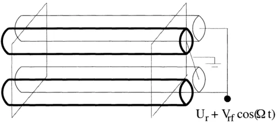
Linear Paul traps consist of four rod electrodes and two endcaps, as shown in
Figure 2-1. Rf voltages are applied to the four parallel electrodes to confine the ions
f
cos(Q t)
I I I I
Figure 2-1: Electrode configuration in a linear Paul trap. Oscillating voltages are applied to one pair of diagonal rods, while DC voltages are applied to the two
endcaps. [WMI+98]1
radially in an oscillating quadrupolar electric field. The ions sit at or near the nodal line of the rf field. The voltages applied to the endcap electrodes create a static potential which confines the ions axially.[Ber01] The entire trap is under ultra high
vacuum of pressures less than 10-10 Torr to avoid loss of trapped ions due to collisions.
The ions are produced by pointing an electron gun at a strontium oven within the trap. The electron gun is made from tungsten wire, and the oven contains solid
strontium enclosed in a sheet of tantalum foil. Heating the oven fills the trap chamber
with neutral strontium vapor. Electrons produced by the electron gun ionize the vapor, and the ions are then trapped. A picture of the electron gun and strontium oven used in our ytterbium trap is shown in Figure 2-2. The strontium trap electron
gun and oven are of the same design.
The second phase involved in building an ion trap is the construction of a laser
system. This step will be described in detail in sections 2.2 and 2.3. The final step necessary to build a working ion trap is the implementation of a detection system. Our
strontium system uses two different detection schemes. The first is a high resolution CCD camera which images the ion cloud. Figure 2-3 contains a CCD image of a
' /
ff ,
Figure 2-2: Photograph of the electron gun and oven used in our ytterbium ion trap which is a copy of the strontium trap. In the upper figure, the leftmost object is the gun, the middle object is a shield used to collimate the ions leaving the oven, and the rightmost object is the ytterbium oven. The lower figure shows the actual ion trap. The oven is above the central rods and the electron gun is below the rods.
trapped strontium ion crystal. The second is a photomultiplier tube which measures
ion fluorescence.
2.2 The Strontium Ion
In order to build a laser system for a strontium ion trap, it is necessary to understand the electronic structure of the strontium ion.
2.2.1
88Sr+ Energy Levels
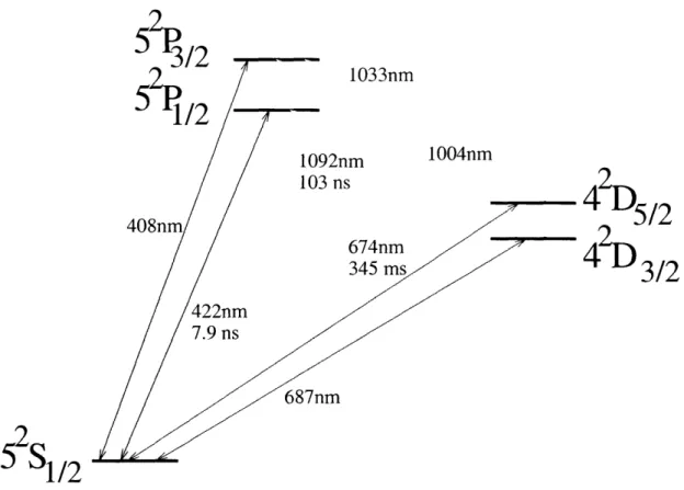
A diagram of the partial valence energy level structure for the 8Sr+ ion is given in
x -.5_ -0 1 2 3 4 5 6 7 B 9 10 trap x-axis (mm)
Figure 2-3: Image of a trapped strontium ion crystal produced by the CCD camera.
line is the 5251/2 52P1/2 transition. This line has a wavelength of 422 nm and is
the fluorescing transition. It is used for ion detection and cooling.
Ions in the 52P1/2 state have a finite probability of decaying to the 42D3/2 state
instead of fluorescing to the 52S1/
2 state. Therefore, it is necessary to have a repump laser tuned to this transition at 1092 nm in order to avoid depopulating the principal transition.
The final transition of interest is the 52S1 /2 -- 42D5/2 transition at 674 nm. The
laser built for this line is the focus of this thesis, and the specifics of this line are described in Section 2.2.3. This line will be used as a temperature probe and an
optical qubit in our experiment.
2.2.2
Uses of the 674 nm Line
The 674 nm transition is of particular interest because of its many potential and
previous uses. The 674 nm line was used to test the randomness of quantum mechanics in an experiment performed by D.J. Berkeland, D.A. Raymondson, and V.M. Tassin that is described in detail in Reference [BRT04]. In this experiment, single 8 8Sr+ ions were trapped in a linear Paul trap. Three lasers of wavelength 422 nm, 1092 nm, and
674 nm were applied to the trap, and the fluorescence at 422 nm was continuously
521 , 3 10Q2n 1033nm m 1004nm 2D
D512
4% 3/2
I2--'
1/2
Figure 2-4: Energy level diagram for the SSSr+ ion. The exact wavelengths of the three
transitions of interest in our experiment are: 421.671 nm in vacuum, 421.552 nm in air for the blue transition, 1091.787 nm in vacuum, 1091.488 nm in air for the infrared
transition, nd 674.026 nm in vacuum, 673.842 nm in air for the red transition.
at 422 nm was observed, whereas if the ion was not in the D5/2 state, fluorescence
was observed. According to quantum mechanics, the results of such a measurement
should be unpredictable. By applying statistical tests to the fluorescence signal data, this experiment reduced the uncertainty in the randomness of the quantum jump
effect by over an order of magnitude.
The 674 nm line of 8SSr+ is also a promising candidate for use in an optical clock, which works on the same principle as an atomic clock.[MBH+05] In an optical clock,
the oscillator is a laser stabilized to an atomic transition in the visible spectrum, while
in atomic clocks, the transition is in the microwave regime. Visible transitions have
higher frequencies than microwave transitions, but the two types of transitions have similar widths. Therefore, optical clocks offer greater stability than atomic clocks.
The 52S1/2
,-
42D5/2 transition in 88Sr+ is currently the most accurately measuredoptical frequency standard in the world. Its frequency is known to an accuracy of 1.5 Hz, or 3.4 parts in 101 5.[KBG+03] Work is being done at the National Physical
Laboratory of the United Kingdom and elsewhere to show that this standard is more stable than the cesium standard. This work could lead to an optical redefinition of
the second based on the 674 nm line of 8 8Sr+.[MBH+05]
Another use of the 674 nm line is as a temperature probe for trapped ions. The 52S1/2 -> 42D5/2 transition is useful for this purpose because it is not a cooling
tran-sition. After the trapped strontium ions have been laser cooled to a low temperature, the 674 nm laser can be swept. In the many ion regime, the temperature can be
calculated from the Doppler width of the spectrum. In the single ion regime, there should be a sharp peak at zero detuning and smaller peaks at integer multiples of
the secular frequency of the ions. The temperature of the ions can be calculated by
measuring the ratio of the peaks.[DBIW89]
Finally, the 674 nm line can be used as an optical quantum bit, or qubit, with
the 52S1/2state acting as the logical '0' and the 42D5/2 state acting as the logical '1.' This is the most important application of the 674 nm transition for the purpose of
building an ion trap quantum computer. The 52S1/2 -* 42D5/2 transition is a good
candidate for a qubit because it has a very long lifetime.
There are actually two lines in 8 8Sr+ that could be used as the optical qubit. Initially, we chose the 52S1/2 - 52P1/2 transition to use as the imaging and cooling
transition because the 52P1/2state only decays to the 42D3/2state, whereas the 52P3/2
state decays to both the D states. By using the 422 nm transition, we only need one
repump laser instead of two. Given this initial set-up, the 52S1/2 -+ 42D5/2transition
is a better candidate for use as a qubit than the 52S1/2 -÷ 42D5/2 transition, even
though both have long lifetimes, because the 42D
3/2 state is being repumped to the
2.2.3
Specifics of the 674 nm Line
The most accurate frequency measurement of the 52S1/2 -4 42D5/2 transition is
444 779 044 095 484.6(1.5) Hz [MBH+05], corresponding to a vacuum wavelength of 674.025591 nm and a wavelength in air of 673.842 nm. The 52S1/2 - 42D5/2
tran-sition is an electric quadrupole trantran-sition, making it 108 times less likely than an
electric dipole transition. Therefore, it has an extremely long lifetime of 345 ms and an extremely small linewidth of 0.4 Hz.
2.3 External Cavity Diode Lasers
External cavity diode lasers have a number of useful properties that make them suited for the 674 nm laser in our experiment. This section describes the theory and properties of external cavity diode lasers.
2.3.1 Laser Theory and Properties
In order to understand how lasers work, one must understand the ways in which
light interacts resonantly with matter: spontaneous emission, stimulated emission,
and absorption. Spontaneous emission occurs when an atom decays from the higher energy level to the lower energy level of a two-level system without any outside stimuli
inducing this energy change. The change can occur through the emission of a photon
of frequency v, where
=
(E2 - El)/h.
(2.1)
E2 is the energy of the upper state, E is the energy of the lower state, and h is Planck's constant. Non-radiative decay is also possible due to collisions, etc. with the extra energy increasing the kinetic energy of the atom. This process does not contribute to lasing, however. If a photon is emitted during spontaneous emission, its direction and phase are random.[Sve89]
Stimulated emission occurs when an electromagnetic wave of frequency v is inci-dent upon an atom in the higher energy level. The atom switches from the higher
energy state to the lower energy state by emitting an electromagnetic wave that is
in phase with the incident wave. In this way, the emitted wave adds to the incident
wave.
Electromagnetic radiation can also be absorbed by an atom, of course. In the absorption process, a photon of frequency v is absorbed by an atom in the lower
level, thereby raising the atom to the upper energy level.
In order to make a laser, population inversion, in which the number of atoms in
the excited energy level exceeds the number in the ground state, must be achieved. Population inversion cannot be achieved by absorption alone because stimulated and
spontaneous emission decrease the number of atoms in the upper energy level. In addition, population inversion cannot be achieved in a two-level system because the
probabilities for absorption and stimulated emission are the same. In order to produce
population inversion, a higher number of levels must be used. Figure 2-5 illustrates three-level and four-level systems for producing laser action. In a three-level system,
A
3
A4
fast decay
', fast decay
pump
3
-
23
<
-pump
2p3
laser
pump
laser
1
'~
2
, ,~~~/
'fast decay
1
Figure 2-5: Three and four energy level systems for producing population inversion.
the atoms are pumped from level one to level three where they undergo fast decay to level two. The laser action occurs between levels two and one. In a four-level system, the atoms are pumped from level one to level four where they undergo fast
undergo fast decay from level two to level one. The four level system is more efficient
for producing population inversion because the laser action occurs between excited energy level states, states two and three, and state two is initially unpopulated..
Figure 2-6 contains a diagram of the basic materials needed to make a laser. The
RI K V V V V V
mirror
-
-1-
partially reflective
mirror
Figure 2-6: Experimental set-up of a generic laser.
active material is placed in a resonant cavity between two mirrors, one of which is
partially reflective. The cavity is designed so that the laser wavelength corresponds
to one of its resonant modes. Once the threshold population inversion is achieved,
spontaneous emission will start the lasing action. The threshold population inversion,
N2 -N1, is
N2 - N - (RR2 ) (2.2)
2al
where R1 and R2 are the power reflectivities of the mirrors, r is the stimulated
emission cross section, and is the length of the active material.[Sve89] Each time an
electromagnetic wave passes through the active material, it is amplified.
There are four properties of lasers which make them useful sources of light for
experimental purposes. The first property is monochromaticity. Only electromagnetic
waves of frequency v corresponding to the difference in energy between the two laser states and to a resonant frequency of the cavity can be amplified, resulting in a very
narrow linewidth of laser light. Lasers also produce both spatially and temporally
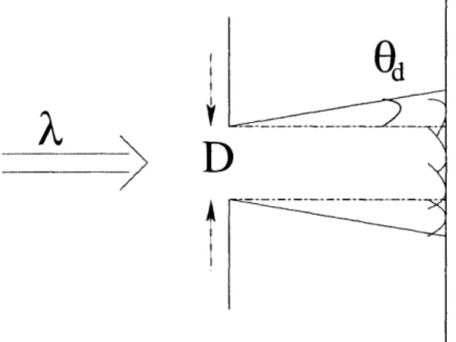
coherent light. Lasers have a third property of directionality. Laser beams are in
theory diffraction limited, meaning their angle of divergence is
Od = /A/D (2.3)
where A is the laser wavelength, D is the width of an opening through which the beam
passes, and d is a parameter which depends on the shape of the amplitude distribution
(see Figure 2-7). The final important property of lasers is brightness, defined as
__ D
I
Figure 2-7: Illustration of a diffraction limited beam.
the power per surface area per solid angle. Lasers have orders of magnitude higher brightness than conventional light sources because of their high directionalities. [Sve89]
2.3.2 Diode Lasers
Diode lasers offer several advantages over other laser mediums which make them a suitable choice for the 674 nm laser. Diode lasers are inexpensive, small, and
compact. The diode chip itself has typical dimensions of 300x250x125 ,um, and the
package is typically about xlx0.5 cm[L'H05] (see Figure 2-8). Diode lasers have high efficiencies up to or above 20% and long life expectancies usually on the order of 50,000 hours.[L'H05] They have no internal optical elements and require no
spe-cial laboratory facilities to operate. They are also inherently capable of terahertz
[e
Window
Figure 2-8: Diagram of a laser diode package, reprinted from [L'H05] without per-mission.
15 nm).[Cam85]
A laser diode is an electronic device made from a semiconductor p-n junction.
Laser action can be achieved in a p-n junction formed by two or more doped semi-conductor layers, as shown in Figure 2-9. If an injection current is applied through
the p-n junction, carrier recombination will occur in the depletion area between the p-type and n-type layers.[L'H05] The recombination process in the junction produces incoherent light. Above a certain current threshold, photons moving parallel to the junction can stimulate emission and initiate laser action.[NavO5]
Laser diodes produce highly divergent light because the cross-sectional
dimen-sions of the lasers' active regions are on the same order of magnitude as the lasing
wavelength. Therefore, collimation of the beam is required.
Diode lasers have typical linewidths of ten to one hundred megahertz.[Cam85]
This linewidth can be reduced by using an external cavity diode laser apparatus as
described in Section 2.3.3.
The 674 nm laser is made from a multi-quantum well laser diode. Quantum well laser diodes are made by reducing the thickness of the active region to 10 nm or less.
Highly Partially
reflective reflective
end end
De
re
Figure 2-9: A laser diode made from a p-n junction reprinted from [NavO5] without
permission.
important because the energy levels in the band gap are quantized. The degrees of
freedom of the charge carriers are limited to two dimensions.[L'H05] This produces a
higher gain at much lower threshold currents.[Sil96]
2.3.3 External Cavity Diode Lasers
Diode lasers typically have linewidths on the order of ten megahertz or greater. The
use of a diffraction grating in an external cavity can provide better resolution, based
on the relation
Av x L 2 (2.4)
where Lop is the optical length of the cavity. [L'H05] This typically reduces the linewidth
to around one megahertz, although linewidths as small as one hundred kilohertz can
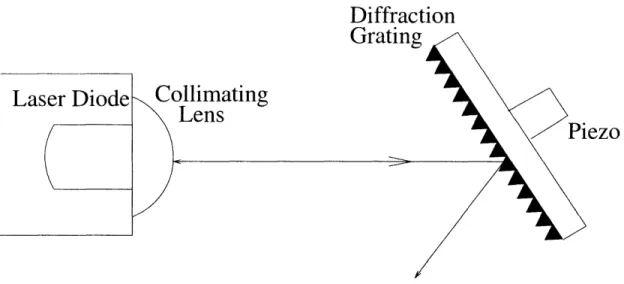
be achieved. This setup is known as an external cavity diode laser (ECDL), and is illustrated in Figure 2-10. In an ECDL, the collimated beam leaving the laser diode
travels through an external cavity and bounces off a diffraction grating. The grating
diffracts certain wavelengths back into the diode. The desired wavelength can be
Diffraction
d ) a,
Collimating
\ Lens
Figure 2-10: Diagram of the components involved in an external cavity diode laser. A grating is used in an external cavity to select a wavelength with fine resolution.
The first order is used as feedback and the zeroth order is used as the output.
a piezo-electric device, as shown in Figure 2-10. The first order is fed back into the
diode and the zeroth order is used as the output.
In atomic physics experiments, picometer precision of the laser wavelength is often
needed. Therefore, tuning is an essential element of building a laser. There are several factors that determine the single mode lasing frequency of an ECDL. The laser diode medium gain has the broadest profile with typical widths on the order of 5000 GHz. The grating profile has a width of about 50 GHz. The internal cavity modes are separated by about 60 GHz. The external cavity modes offer the finest resolution with separations of about 10 GHz.[AG01] The interplay of these structures determines the
lasing wavelength, as shown in Figure 2-11.
There are several controls which can be used to adjust the previously mentioned structures i order to select a particular wavelength. The grating profile can be shifted by adjusting the position of the grating manually. Applying a voltage to the piezo-electric device changes the external cavity length by changing the distance from the laser diode to the grating. Changing the temperature of the laser environment shifts all of the previously mentioned profiles. Finally, the injection current can be adjusted for fine-tuning. The current affects the internal diode cavity length by changing its
~FREUENCY . I < EMITED FEOUENCY
FREQ::UENCY
--Figure 2-11: The ECDL mode structures that determine the single mode laser wave-length, reprinted from [AG01] without permission.
temperature as a result of Joule heating. Below threshold, the current has a larger effect on the internal cavity length because the laser's refractive index depends on the charge carrier density. Above threshold, however, the carrier density is saturated, and the current can only affect the cavity length through Joule heating.[Sve89]
I4EDIUMGAf4
WIDTH- 5M0 GHz `
GRATING PROFILE
INTERNAL MODE /- NA MO
Chapter 3
Construction of the Laser
Apparatus
This chapter describes the process of building the laser apparatus. It begins with a description of the selection of the specific laser diode used. Next, the setup and design of the laser diode box are described. The performance of the laser, specifically, the power output, is presented, followed by a section on the construction of the temperature controller. Finally, the optical breadboard layout is shown and the individual components used to tune and collimate the beam before it enters the ion trap are explained.
3.1 Selection of the Laser Diode
The selection of the specific laser diode to use for the 674 nm laser was made easy by the availability of a very convenient choice. The selected diode is a Hitachi HL6724NIMG
AlGaInP laser diode that is available commercially for approximately twenty dollars. Figure 3-1 contains a picture of the diode package.
The selected diode had a multi-quantum well structure. Its typical output power is 5 mW, and its typical wavelength is 670 nm. The expected threshold current is 25 to 35 mA, and the typical operating current is 35 to 50 mA.[Hit97]
Figure 3-1: The laser diode package, reprinted from [Hit97] without permission.
3.2 The Diode Laser Box
The setup of the diode laser box is based on a design by Viadan Vuletic outlined in Reference [RWE+95]. The dimensions of some of the components involved are shown in the diagram in Figure 3-2. The laser diode package sits in a small mount. The diode
mount is glued to an aluminum mount containing a collimating lens. The collimating
lens sits about one millimeter away from the edge of the glass window on the diode
package (see Figure 2-8). The diode mount is attached to the upper aluminum base
plate by a nut and bolt. The edge of the lens mount is 1.3 cm away from the edge of
the diffraction grating. The grating is glued to a piezo-electric actuator. The other
end of the piezo-electric actuator is glued to an adjustable mount which is affixed to
the opposite end of the upper base plate with a nut and bolt.
The upper base plate is attached to the lower base plate by four plastic nuts and bolts so that the two plates are electrically and thermally isolated. A thermoelec-tric cooler (TEC) sits between the two plates. A thermistor, used to monitor the
temperature, is glued in a small hole in the upper base plate.
The thermistor, TEC, piezo-electric actuator, and laser diode are all connected to
external BNC cables mounted on the walls of the laser box. A capacitor is connected
(a)
/1,
A ku) , t~~~~~~~~~~~~~~~~~~~~~~~~~~~~~~~~~A 1.4 cm: 4 | sou. cm 10.8 cm 1.2 cm l.. 6.60 cm I ... 'AA IM - - -- 5.69 cm < 6, 36 em- - - - -- - - - --~-:~ V --- 11.47 cm---.Figure 3-2: Diagram of the laser box layout. (a) The inside of the box. (b) The lens mount. (c) The box cover.
across the terminals of the thermistor to filter out high frequency noise. The laser
diode is connected to a switch for protection. A photograph of the inside of the laser box with the components labeled is shown in Figure 3-3.
An aluminum cover encases the laser box. It has a small hole drilled in the side
to let out the laser beam (see Figure 3-2).
3.3 Laser Performance
The laser performance was tested by measuring the power output as a function of injection current for several different temperatures. According to theory, the power should behave as a linear function of injection current both at currents lower than the threshold and higher than the threshold. The slope of the power output vs. injection
current curve should be much smaller for currents below the threshold. [Cam85] There-fore, a graph of power output vs. injection current should have two linear regions
with a kink at the threshold lasing current.
. 5 cm ---upper plat diode mlunt
, _
Ž< )collmdting
0.9 cmI\< lens m unt 7.5 cnj 1.3 cn jezoratig lower te -f
gaigount
lower plte- 5.03 cm , __ .--- .1 33 cm T7 : 2.52 cm V I FA 11 14 1 -I I JFigure 3-3: Photograph of the inside of the laser box.
The 674 nm laser behaved exactly as expected. Figure 3-4 contains graphs of
the power OluLtpUt vs. injection current at three different temperatures. Two linear fits have been applied to each graph; one for the data at currents below threshold,
and one for the data at currents above threshold. The slope of the data for currents above threshold is higher than the slope of the data for currents below threshold,
as predicted. Our typical operating current is 50 mA in order to achieve an output power of about 5 mW.
3.4 The Temperature Controller
The TEC is controlled by a Wavelength Electronics PID 1500 temperature controller.
A TH10K thermistor from Thorlabs is used to monitor the temperature. The TH10K is a 10 kQ thermistor with a 1"C accuracy. A photograph of the temperature controller
is shown in Figure 3-5.
E 6 S o 4 CQ current 30 (mA)2 4 current (mA) 6 Es o ,Es U) 0 current (mA) 0 I 20 c 30 40 current (mA)
Figure 3-4: Power output vs. injection current at 10.8°C, 20°C, and 30°C (left to right). The red line is a linear fit of the data below threshold; the green line is a
linear fit of the data above threshold.
y = 0.3310*x -10.7174 y = 0.0009884'x -0.005312 . y = 0.3386*x -11.7797 y = 0.001177'x -0.007963 _ y = 0.3786x -14.6288 y = 0.001525'x -0.01325 I J _ : 5 _ I 10 20 30 40 5 ! . 2 n o)0 . 50 6 7 2 8 ; 50 6
Figure 3-5: Photograph of the temperature controller.
PID stands for proportional with integral and derivative control. PID controllers
work by turning the output on and off in a ratio of the measurement difference from
the set point temperature in the proportional band, set by the parameter p. The integral control integrates the deviation signal with respect to time. The integral is summed with the deviation signal to shift the proportional band. The derivative control shifts the proportional band to compensate for rapidly changing temperature. The amount of shift is proportional to the rate of the temperature change.[Eng00]
The Wavelength Electronics PID 1500 allows the user to set p, and it automati-cally determines the integral and derivative parameters. With p set to 30, the laser
box temperature stabilized to an offset of 0.007 V, corresponding to 0.16°C, from
the set point temperature. Fluctuations in the temperature of less than 0.0001 V,
corresponding to less than 0.002°C, were observed. Figure 3-6 contains a graph of
the temperature of the laser box as a function of time, illustrating the behavior of the temperature controller.
3.5 Optical Breadboard Layout
The final step in the construction of the 674 nm laser was the design and layout of the
optical breadboard. A photograph of the optical breadboard is shown in Figure 3-7.
The laser box is attached to the optical breadboard using a block of sorbothane to minimize vibrations. The beam leaves the laser box and is raised to a height of
0 U) CU > U) E U) O 5 0 01 150 20 250 300 350 4OO 450 O time (seconds)
Figure 3-6: Graph of the set temperature and actual temperature vs. time. Blue is the set temperature; red is the actual temperature. 1 Volt corresponds to 25°C, and
a difference of 0.01 Volts in this regime is equal to approximately 0.2°C.
13.8 cm by a two-mirror periscope. The beam travels through an optical isolator and through the first beam splitter. The first beam splitter sends 10% of the beam to a mirror and the rest of the beam through the second beam splitter. The beam reflects off the mirror into a Fabry-Perot cavity. The output of the Fabry-Perot cavity is monitored by a photodiode. The second beam splitter sends 10% of the beam to the
first optical fiber and the rest of the beam to a mirror. The first optical fiber sends the beam to the wavelength meter (Coherent WaveMaster). The rest of the beam
reflects off of the mirror into the second optical fiber. The second optical fiber sends
the beam to the ion trap.
There are two other components on the optical breadboard as well. The first is the temperature controller, and the second is a motorized shutter located in between the final mirror and the second optical fiber. The shutter can be configured so that it either blocks the beam or lets it into the second optical fiber.
1. . . . -1- ; . :1 YI I 11- j i i: . I ji 1%1 II f LI -1- I
Figure 3-7: Photograph of the optical breadboard.
36
IR
Chapter 4
Tuning the Laser
This chapter describes the process of tuning the 674 nm laser to the precise wavelength of 673.842 nm in air. Four variables used to tune the laser are described in detail. First, the temperature dependence of the threshold lasing current and wavelength is
explored. Second, the processes of using the grating and the piezo voltage to
fine-tune the laser are described. The chapter concludes with a section on the Fabry-Perot resonator in which theory and measurements are explained.
4.1 Temperature Dependence
Temperature is a very important parameter for tuning an ECDL because all of the factors that determine the laser wavelength depend on the temperature (see Sec-tion 2.3.3). A diode laser's threshold current is a sensitive funcSec-tion of temperature as
a result of several different mechanisms. Therefore, there is no single expression for
the temperature dependence of the threshold lasing current, although the relationship
is often approximated as a simple exponential:
Ith (T) = I T/o (4.1)
where Ith is the threshold lasing current, T is the temperature, and Io, and To are
threshold lasing current vs. temperature. Approximating the data by an exponential
yields a fit with 1% error.
38 37 : 36 u 35 34 33 y = 29.06,e"',1°9 I I I ~~~~~~'/ II I 10 12 14 16 18 20 22 24 26 28 30 temperature (C)
Figure 4-1: Temperature dependence of the threshold lasing current.
An analytical relationship between the wavelength and temperature of a diode laser is also difficult to calculate. The internal cavity modes are temperature
de-pendent because of the temperature dependence of the refractive index. The gain
profile is also temperature dependent because of the temperature dependence of the bandgap. As a diode laser's temperature is raised, the gain curve shifts to higher wavelengths faster than the cavity modes. When a particular mode no longer has enough gain to lase, the wavelength mode hops to a mode where the gain is sufficient. Therefore, the wavelength vs. temperature curve should have a 'staircase' shape with mode hops corresponding to cavity mode spacings. [Cam85] Figure 4-2 contains a plot of lasing wavelength vs. case temperature taken from the Hitachi HL6724MG speci-fication sheets. [Hit97] This plot was made before the laser was locked to a diffraction grating or external cavity. The staircase shape is evident.
I---,.-.,,,-,,- . .. . ...-. ... ... ... . ... ... ...
682 E
c
o.. U) -:5 : ¢ a)a) (/) ._ M 680 678 676 674 672 670 668 0UU -10 0 10 20 30 40 50 Case temperature, T (C)Figure 4-2: Plot of the lasing wavelength vs. case temperature reprinted without
permission from the Hitachi HL6724MG specification sheets.[Hit97]
4.2 Tuning with the Grating
The external cavity uses a GR13-1850 ruled refractive grating from Thorlabs pictured in Figure 4-3. The grating has 1800 grooves per millimeter and a blaze wavelength
Figure 4-3: Diffraction grating used in the external cavity to tune the laser wave-length, reprinted from [Tho05] without permission.
of 500 nm. The diode itself is a distance of approximately 2.2 cm from the face of the grating (see Section 3.2 for a diagram). According to the grating equation for the
Littrow configuration, the first order diffracted wavelength as a function of grating
I I PO= 5 mW
_r
// / . . . aizaposition is
A(0) = - sin(01) (4.2)
g
where g is the number of grating lines per meter, and 01 is the angle between the
incident beam and the grating normal.[SewO4] Figure 4-4 contains a diagram which illustrates the relevant parameters.
Grating
A
Len
Len
Figure 4-4: Diagram of the grating, lens, incident beam, and reflected beams.
The grating tuning profile is governed by the phase overlap, or interference, of the
incident and reflected beams. The magnitude of the phase overlap is given by
P
= de-i(k1-k2)xdx (4.3)where L is the size of the output mode, k is the wave vector in the x-direction for the exact reflection, and k2 is the wave vector for small angle reflection. To a good
approximation, k = 0, and k2 = ksin(02). Using this approximation, Equation 4.3
simplifies to
L 2
p =
J
e-i2 /sin(O)xdx (4.4) This relationship is graphed in Figure 4-5 for small angles. Equations 4.2 and 4.4 canol 08 ,/ 07 / 03 / 0o Cd) -105 -1 -05 0,r~ias 05 1 01 5 -( r adans) ,1o
Figure 4-5: Graph of the diffraction grating tuning profile.
673.842 nm, the grating profile has a width of about 70 GHz.
4.3 Piezo Tuning
The piezo-electric actuator is used to fine tune the laser wavelength with picometer or smaller resolution. The piezo transforms an electrical signal into mechanical motion.
Applying a voltage to the piezo causes the position of the grating to change by a small
amount, and therefore the length of the external cavity changes by a small amount.
In this way, the laser wavelength can be tuned.
When we first tried to tune the 674 nm laser wavelength using the piezo, chang-ing the piezo voltage caused discrete mode hops of the laser wavelength instead of
continuous tuning. This problem was solved by inserting an optical isolator into the
beam path, as described in Section 3.5. Optical isolators remove back reflections by allowing light to travel in only one direction. Back reflections create feedback and
act as an unintentional external cavity. This prevents continuous tuning of the laser
wavelength.
After the optical isolator was inserted, the laser wavelength tuned continuously with the piezo voltage. The maximum continuous tuning range is about 9 pm be-tween mode hops. Under a wide variety of conditions, the tuning rate was measured to be between 0.38 and 0.48 GHz/V. These conditions included different operating
temperatures, injection currents, and output powers. Figure 4-6 contains an example
of a wavelength vs. piezo voltage tuning curve.
55 5.
o
4.5 4 ., = y -0.48*x + 1.69 4 P 35. LL O 2 I,,1.
5
IE
m;I
-7 6 -5 -4 -3 -2 -1 0 Piezo Voltage (V)Figure 4-6: Graph of laser wavelength vs. piezo voltage. The blue points are the data,
and their staircase form is due to the limited resolution of the wavelength meter. The
red line is a linear fit to the data.
4.4 The Fabry-Perot Resonator
A Fabry-Perot resonator is an extremely useful and important component of a laser
system. Fabry-Perot resonators offer high resolution of the laser frequency and can
function as interferometers. We hope to eventually frequency lock the 674 nm laser
to a Fabry-Perot cavity. The type of Fabry-Perot cavity used in our experiment
consists of two partially reflective spherical mirrors, as shown in Figure 4-7. In this configuration, the two mirrors are often in a confocal arrangement in which they are
located a distance apart that is equal to their radius of curvature. The interference fringes at the output of the mirrors form concentric circles.
The free spectral range, defined as the frequency distance between two spectral
maximums of interference, is an important parameter used to describe Fabry-Perot cavities. The path difference for beams traveling close to the center of the mirrors is 4 times the distance between the mirrors (see Figure 4-7). The free spectral range,
d
Figure 4-7: A Fabry-Perot cavity consisting of two mirrors. The arrows illustrate the beam path.
then, is given by
C
d>= 4d (4.5)
4d
where c is the speed of light, and d is the distance between the two mirrors. A second important parameter is the finesse which is a measure of the resolving power of the Fabry-Perot interferometer. The finesse is defined as
3v
F= A, (4.6)
AV
where /v is the full width at half maximum of a resonant peak.[Hau84] Based on this definition, the finesse can also be expressed as a function of the reflectivity, R, of the mirrors (see Reference [Hau84]):
F= 1R (4.7)
Figure 4-8 is a photograph of our Fabry-Perot resonator. The distance between the two mirrors is approximately 14.3 cm. This arrangement is not quite confocal. The reflectivity of the mirrors is 95%. According to Equations 4.5 and 4.7, the free
spectral range should be 524 MHz, and the finesse should be 61.
We took several scans to determine the experimental free spectral range and finesse of our Fabry-Perot resonator. We scanned the piezo voltage to modulate the laser wavelength and monitored the output of the photodiode. Figure 4-9 is a plot of one
such scan. The average resonant peak spacing of the Fabry-Perot signal shown in Figure 4-9 is 519 MHz. Considering that our wavelength meter has a resolution of
Figure 4-8: Photograph of the Fabry-Perot resonator. The photodiode is on the left and a mirror is on the right.
Frequency and Fabry-Perot Signal vs. Piezo Voltage - 0.40 GHzN
7 -Ci IL Cr 3 0 -8 -7 -6 -5 -4 -3 -2 -1 Piezo Voltage (v)
Figure 4-9: Frequency and Fabry-Perot signal vs. piezo voltage. The green curve is
the Fabry-Perot signal, the blue points are frequency vs. piezo voltage data, and the
red line is a linear fit to the data.
only 100 MHz, this value of the free spectral range compares well to the prediction.
Our cavity has a relatively low finesse of about 10, which is much smaller than
the predicted value. This is almost certainly due to the fact that our mirrors are not
confocal, and, therefore, the limiting finesse is lower than the reflection finesse.
The resonant peaks in Figure 4-9 are not spaced exactly evenly. This is mostly due to the fact that the laser wavelength was drifting continuously at a rate of about
15 MHz per minute in addition to the drift caused by scanning the piezo voltage.
In the future, we hope to isolate the laser from ambient temperature fluctuations in order to reduce this drift and lock the laser to the Fabry-Perot cavity.
Chapter 5
The Depletion Experiment
This chapter describes the experiment to find the 674 nm transition in 88Sr+. As described in Chapters 3 and 4, the red laser is tunable to the predicted wavelength of the transition in air. The next step is to find the transition in the trapped stron-tium ions with the eventual goal of using the 674 nm laser in quantum information experiments.
The idea of the depletion experiment uses both the blue and red transitions in
88Sr+. The blue transition fluoresces at 422 nm. When the red laser is on, the red
transition depopulates the blue transition, decreasing the fluorescence. We should be
able to turn the red laser on and off and see the ion signal "blink" as a result of the changes in fluorescence.
This chapter begins with some theoretical predictions associated with the deple-tion experiment including the predicted linewidth broadening values of the red laser and the required resolution. Next, the experimental procedure is described. Finally, some preliminary data and results are given.
5.1 Theoretical Predictions
Before performing the experiment, we needed to determine its feasibility by calcu-lating the resolution required to produce an observable change in fluorescence signal. The Doppler broadened linewidth of the trapped ions at room temperature is about
1 GHz. Linewidths as low as 30 MHz have been achieved with laser cooling, however.
The linewidth of the 674 nm laser is broadened by several mechanisms. The first is power broadening. Power broadening occurs in a two-level system by shortening the
lifetime of the excited state due to stimulated emission.[Tis96] The power broadened linewidth can be expressed in terms of the saturation intensity:
7'= 7V/1
+ I/Is
(5.1)
where y' is the power broadened linewidth, 7-y is the natural linewidth, I is the intensity, and I is the saturation intensity. [MvdS99] The saturation intensity is the intensity at which spontaneous emission is equal to absorption in the system and can be calculated
from
i-hc
I= 3A3'- (5.2)
where h is Planck's constant, c is the speed of light, A is the wavelength, and T is the
lifetime of the transition.[MvdS99]
The 674 nm transition has a very long lifetime (see Section 2.2.3), so its saturation intensity is very low: I = 2 x 10- 1 ° W/cm 2 compared to 0.03 W/cm2 for the 422 nm transition. This gives the 674 nm atomic transition a very low power broadened linewidth of about 2 kHz at a power of 1 mW, compared with about 100 MHz for the 422 nm laser at the same power.
If power broadening were the only broadening mechanism involved, we would need extremely high laser and ion stability in order to observe depletion in the ion signal, because the 674 nm laser could only interact with on the order of one ten-thousandth
of the Doppler broadened ion sample at a time. However, there are other broadening mechanisms associated with the physics of the laser diode itself that increase the
674 nm laser linewidth to about 1 MHz. The actual linewidth of the laser is described by the Schalow-Townes formula (see Reference [Sve89]). The spectral broadening of
the laser arises from phase and amplitude fluctuations of the output power due to
spontaneous emission noise. [Sve89]. In diode lasers, the linewidth is broadened by an
index of refraction changes that result from changes in the carrier density. This leads to approximately an order of magnitude increase in the linewidth.[Cam85]
The actual laser linewidth is broadened to about 1 MHz by the previously
men-tioned mechanisms. Therefore, with some cooling of the ions, we would need a laser stability of about one part in one hundred to see a change in the fluorescence signal. It should be noted that a change of one part in one hundred in the ion signal repre-sents a tiny change in the frequency of the 422 nm and 1092 nm lasers, making the depletion experiment difficult without first frequency locking the lasers. For example, change of 10 MHz in the blue laser frequency can cause up to a 15% change in the ion signal intensity.
5.2 Experimental Method
Three different kinds of scans were taken in order to search for depletion in the fluorescence signal. The first step of the experimental procedure is the same for all three scans. Ions must be loaded into the trap, and the fluorescence signal is
monitored. The 422 nm and 1092 nm lasers are fed into the trap, but the 674 nm
laser light is blocked. In the first type of scan, the red laser light is then unblocked and the piezo voltage is slowly scanned to modulate the red laser wavelength. Once every second, the ion fluorescence signal is measured and recorded by the CCD camera. The red laser frequency is also recorded. If the 674 nm transition has depopulated
the 422 nm transition, there should be a dip in the ion intensity signal at a particular
frequency of the red laser.
In the second type of scan, the blue laser is used to cool the trapped ions before the red laser light is unblocked. Next, the red laser light is unblocked, and the red laser
wavelength and blue laser wavelength are scanned simultaneously while measuring the ion fluorescence with the photomultiplier tube. The ion intensity signal is graphed as
a function of both red and blue wavelength.
In the third type of scan, an ion crystal is formed before unblocking the red laser. Crystallizing the ions should help to decrease losses and improve ion signal stability.
The red laser is then unblocked, its wavelength is scanned, and the ion intensity signal
is measured and recorded over the length of the scan by the photomultiplier tube.
5.3 Data and Results
An example plot of the first type of scan is shown in Figure 5-1. The bottom plot
50 100 150 X 10 50 100 150 200 1 6 , , , , , , , , c 4 Q)1 C .c 2 - -
/
0
-T 9 CD 0 -T r-a) ET ,_= ,;L 7 8 9 10 11 12 13 14 ( X 105 E 9.5 , , , , , , Cx 9 .. '~ -9 . ..~ ~ ~ ~ ~..."--:,-
. ... . ... :...-... 8.5 . . 8O 7 8 9 1 0 1 1 12 13 1 4 7 8 9 10 11 12 13 14 Piezo voltage [V]Figure 5-1: Example of the first type of depletion experiment scan. The top graph is
an image of the ion cloud taken by the CCD camera. The second graph from the top
is a plot of ion intensity vs. trap position. The third graph from the top is a plot of
piezo voltage vs. red laser frequency. The bottom graph is a plot of ion intensity vs. piezo voltage.
in the figure is a graph of ion intensity vs. red laser piezo voltage. There are no dips in the ion signal that are significant compared to the noise in the signal. Also, this scan was performed both by scanning the piezo voltage from high values to low values and from low values to high values, and none of the dips occurred at the same
voltages in both scans. The lack of depletion is probably due to two main factors. First, the CCD camera was averaging the signal over too long of a period, eliminating
any chance of seeing a small but significant decrease in ion intensity. Second, the ion
signal was dlecreasing with time, making it difficult to see a depletion signature over the background drift.
Figure 5-2 contains a plot of the second type of depletion experiment scan. The
Blue vs. Red Frequency Scan
0
a) 0 II m -2 -1 0 1 2 Red Frequency (GHz)Figure 5-2: Example of the second type of depletion experiment scan. The blue laser
frequency and red laser frequency are in units of GHz from their center frequencies. The red laser center frequency is 444778 GHz. The color scale indicates ion intensity,
with blue being the most intense and red being the least intense.
color scale indicates ion intensity, with blue representing the highest intensities and
red representing the lowest intensities. A depletion signal is also lacking from this scan. This is probably due to the steady ion loss over time which can be seen from
the lower amount of blue area on the right of the plot.
Several mportant changes occurred before the third type of scan was taken. First, we were able to crystallize the ions, as previously mentioned. Second, both the 422 nm
and 1092 nm lasers were frequency locked to Fabry-Perot cavities. Both of these
events increased the stability of the trapped ions. The third type of scan has yielded
promising results. Figure 5-3 contains plots of two scans in which a depletion signal may have been seen. The blue laser frequency is also plotted in these scans to show how ion signal loss occurs with detuning of the blue laser. There is a dramatic dip in the ion intensity signal around a piezo voltage of 9.0 to 9.1 V in both plots. The
drastic drop in the ion signal is due to decrystallization of the ions.
One possible mechanism for this decrystallization is depletion of the fluorescing
transition. The red laser causes about one half of the ions to leave the 422 nm transi-tion, and they therefore become uncooled. The rf heating then decrystallizes the ions.
However, other mechanisms could be responsible for the observed decrystallization. On average, decrystallization is seen in about 80% of all of the experiments
in-volving ion crystals. Therefore, there is about a 64% chance that decrystallization
would be seen in two successive scans. If the red laser is not depleting the 422 nm
transition, the decrystallization should, in theory, occur at a random value of the red
laser piezo voltage. However, decrystallization not caused by depletion of the blue
transition is probably correlated with time, which is correlated with the red laser
piezo voltage in our scans. The random decrystallization almost always occurs when the 422 nm and 1092 nm lasers become unlocked from their frequency references. The
reason for optimism about the scans in Figure 5-3 is that the blue and infrared lasers stayed locked to their cavities during the decrystallization. We do not have data on the probability that decrystallization occurs while the blue and infrared lasers remain
frequency locked to their references, but we can say with certainty that this occurs in less than half of all instances of decrystallization. Therefore, we can conservatively estimate that there is an 80% chance that the signal we see is due to depletion by the 674 nm transition.
The preliminary results from the third type of scan are promising. However, more data needs to be taken to determine with certainty that the dip is due to depletion of
the 422 nm transition. We also need to take more scans to determine the exact red wavelength at which this dip occurs.
-_o If 0 15 *1 C E E O.J0L ).05
Red laser piezo [V]
.2) E _i 5 C CiZ En !5
Red laser piezo [V]
Figure 5-3: Plots of possible depletion signals. The blue curves are plots of the signal from a rubidium cell used to monitor the 422 nm laser wavelength vs. the red laser piezo voltage. The green curves are plots of ion intensity vs. the red laser piezo
voltage. The arrows indicate the direction of the scan. The parallel drift in the rubidium and ion signal is due to blue cavity drift. There is a possible depletion
regions in both graphs located near a piezo voltage of 9.05 V when the ions become
Chapter 6
Conclusion
Atomic ion traps are one of the most promising architectures for quantum information processing. Laser systems are an integral part of atomic ion traps. The immediate
goals of this project were to build a 674 nm laser for a 88Sr+ ion trap, tune the laser to the exact wavelength of the 52S1/2 -* 42D5/2 transition in 8Sr+, and find the 674 nm
line in trapped strontium ions by performing a depletion experiment.
The first goal was accomplished as described in Chapter 3. A diode laser was used
in an external cavity with a diffraction grating. The external cavity diode laser was built and tested. Its output power vs. injection curves displayed characteristic laser behavior.
Chapter 4 described the accomplishment of the second goal. The laser
wave-length depended strongly on temperature and the wave-length of the external cavity. These two variables were manipulated to produce the desired operating wavelength
of 673.842 nm in air. The laser could also be continuously tuned over a range of 9 pm
centered at the desired wavelength by adjusting the voltage applied to a piezo-electric actuator attached to the diffraction grating. A Fabry-Perot cavity was also built and tested. Eventually, we hope to lock the laser frequency to this cavity.
Progress toward the final goal of finding the 52S1/2 *- 42D5/2 transition in 88Sr+
has also been made. The red laser beam was directed into the ion trap, and several
different types of scans of its frequency were made in order to find a depletion signal in the ion intensity, as explained in Chapter 5. 8 8Sr+ fluoresces at 422 nm. A dip in


![Figure 2-8: Diagram of a laser diode package, reprinted from [L'H05] without per- per-mission.](https://thumb-eu.123doks.com/thumbv2/123doknet/13808285.441604/25.940.261.690.134.425/figure-diagram-laser-diode-package-reprinted-l-mission.webp)
![Figure 2-9: A laser diode made from a p-n junction reprinted from [NavO5] without permission.](https://thumb-eu.123doks.com/thumbv2/123doknet/13808285.441604/26.940.292.619.136.439/figure-laser-diode-p-junction-reprinted-navo-permission.webp)