A Dual-Laser Interferometry System for Thin
Film Measurements in Thermal Vapor Deposition
Applications
by
Allen Shiping Yin
B.S. Massachusetts Institute of Technology (2011)
Submitted to the Department of Electrical Engineering and Computer
Science
in partial fulfillment of the requirements for the degree of
Master of Engineering in Computer Science and Engineering
at the
MASSACHUSETTS INSTITUTE OF TECHNOLOGY
September 2012
c
Massachusetts Institute of Technology 2012. All rights reserved.
Author . . . .
Department of Electrical Engineering and Computer Science
Aug 10, 2012
Certified by . . . .
Marc A. Baldo
Associate Professor of Electrical Engineering
Thesis Supervisor
Accepted by . . . .
Dennis M. Freeman
Chairman, Master of Engineering Thesis Committee
A Dual-Laser Interferometry System for Thin Film
Measurements in Thermal Vapor Deposition Applications
by
Allen Shiping Yin
Submitted to the Department of Electrical Engineering and Computer Science on Aug 10, 2012, in partial fulfillment of the
requirements for the degree of
Master of Engineering in Computer Science and Engineering
Abstract
Lithography processes harnessing the phase change of the chemically inert carbon dioxide as a resist have been shown as a possible alternative to patterning thin film organic semiconductors and metals. The ability to control the resist’s growth would make the lithography process more reliable and efficient. This thesis seeks to control and observe the physical properties of the carbon dioxide resist via the optical tech-nique of dual-laser interferometry in conjunction with a quartz crystal micro balance (QCMB).
Thesis Supervisor: Marc A. Baldo
Acknowledgments
I would like to first thank my research advisor, Marc Baldo, for his belief in me in the past three years, and for giving me the opportunity and freedom to tackle such a project. I want to thank Matthias Bahlke for his incredible patience in teaching me about vacuum systems and the dry lithography process, his unwavering support and encouragements, and for being an amazing officemate/mentor who seeks to spread his vegetarianism and love for Patagonia gears. I want to thank Phil Reusswig for challenging me to always think rigorously, pushing me in my research and the valuable discussions. Nick Thompson, whose labview knowledge saved me massive efforts; and Carmel Rotschild, who taught me the art of optical alignment inside glovebox were my first research mentors in the Soft Semiconductor group. Hiroshi Mendoza taught me to always be optimistic. I want to acknowledge everyone in the Soft Semiconductor group for showing me what research and scientific rigor is like.
Outside of those that assisted with theory and experimental work, I couldn’t have done this without my roommates and friends, Joe Lane and Nathaniel Salaz-zar, who always supported me during my times at MIT. I’d also like to thank my fellow bboys/friends/mentors, Donny Yi and Joshua Archbold for their support and confidence.
Finally, I’d like to dedicate this thesis to my family, especially my father who has always believed in me.
Contents
1 Introduction 17
1.1 Organic Light-Emitting Diode (OLED) Displays . . . 18
1.2 Motivations for an Alternative Patterning Process . . . 18
1.2.1 Shadowmasking . . . 19
1.2.2 Inkjet Printing . . . 20
1.2.3 Soft Lithography . . . 20
1.3 The Sublimable Mask Lithographic Process . . . 20
1.3.1 Theory of Practice . . . 21
1.3.2 Process Flow . . . 21
1.3.3 Motivation to Control CO2 Deposition . . . 22
2 Theory of Operation 23 2.1 Physical Vapor Deposition . . . 23
2.2 Bragg Interference . . . 24
2.3 Quartz Crystal Microbalance (QCMB) . . . 29
3 Experimental Setup and Procedures 33 3.1 Experimental Setup . . . 33
3.1.1 Vacuum Chamber . . . 33
3.1.2 Chuck and Substrate Holder Design, and Substrate Cooling . 39 3.1.3 Optics . . . 42
3.1.4 Gas Addition . . . 44
3.2 Experimental Procedures . . . 50 3.2.1 Laser Alignment . . . 50 3.2.2 Substrate Cooling . . . 52 3.2.3 Gas addition . . . 53 3.2.4 Data Collection . . . 54 4 Discussion 57 4.1 Experimental Data . . . 57
4.2 Results and Comparison . . . 59
4.2.1 Refractive Index . . . 61
4.2.2 Density . . . 61
4.2.3 Deposition Rate and Crystal Quartz Frequency . . . 62
4.3 For future use . . . 64
5 Conclusion 65
A Figures 67
List of Figures
1-1 A fine-metal mask used for OLED patterning. Each white shape cor-responds to an OLED sub-pixel [20] . . . 19 1-2 Simplified process flow for sublimation lithography (not to scale) (a)
Begin with a colled substrate to facilitate resist deposition. (b) De-sposit resist. (c) Selectively pattern resist. (d) Deposit desired thin film. (e) Lift-off resist leaving patterned thin film. (f) Repeat as nec-cessary to complete device.[1] . . . 21 1-3 A micrograph of the 115µm-tall pillar SU-8 stamp (top) used to pattern
circles of Alq3 (bottom) [1] . . . 22
2-1 Schematic of a typical vacuum thermal evaporation system with a shadow mask to pattern the substrate. . . 25 2-2 Schematic of the light scattering model.The dashed lines are normals
to all the interfaces. . . 26 2-3 An example of dual laser interference signals. The red and blue
wave-forms represent the fluctuating photodetector signals from two laser beams of different incidence angles. Note the difference in periods of the two waveforms, as well as the roughly constant peroid length within a waveform that is the hallmark of constant deposition rate. . . 29 2-4 Quartz crystal as used for QCMB in the experiments. The gray circular
quartz crystals are coated with gold electrodes by vapor deposition. When used in a QCMB, the active area is only the circular part in the center of the front electrode (left: back electrode, right: front electrode). 30
2-5 Typical crystal monitor feedthrough package. The steel tubes provide cooling for the electronics, passing through the steel vacuum flange on the left. The square blocks on the right end contains the driving and sensing electronics, as well as the quartz crystal (the round golden circle) 31
3-1 Functional schematic of the entire system: The box represents the vac-uum chamber and any components inside or within the 6 planes of the box represent the components either within the chamber, or interfaced with the chamber walls (such as flanges). Green lines represent liquid nitrogen (LN2) flow along the arrows’ directions. Red lines represent electrical connections and the signals flow in the arrows’ directions. Blue lines represent the optical signals. Gray lines represent the flow of gas, which follows the direction of the arrows nominally. . . 34
3-2 A: 3D cad drawing of the vacuum chamber mated with the glovebox. B: 3D cad drawing of the complete chamber. C: Photo of the front of the entire assembly. . . 35
3-3 Front-shot photo of the entire assembly. . . 35
3-4 A: Cad drawing of the back panel of the chamber and the cryogenic pump placement. B: Front of the chamber without door handles. C: Front door sliding mechanism. D: Photo of the back of the chamber showing the gate valve and cryo pump placement. E: Photo of the sliding door inside the glovebox. . . 36
3-5 A: Cad drawing of the top of the chamber, showing locations of valves, flanges and feedthroughs. B: Photo of the top of the chamber. C: Cad drawing of the bottom of the chamber, showing locations of the K-cell flange. D: Photo of the bottom of the chamber. . . 37
3-6 A: Cad drawing of the left side of the chamber, showing locations of valves, flanges, and feedthroughs. B: Photo of the left side of the chamber. C: Cad drawing of the right side of the chamber, showing locations of valves, flanges, and feedthroughs. D: Photo of the right side of the chamber. . . 38 3-7 A: Schematic for the chuck. B: Schematic for the substrate holder. . . 40 3-8 A: The chuck is attached onto the top of the chamber via nylon screws
and nuts. The substrate holder is screwed onto the bottom of the chuck. LN2 flows through the insulated inlet (see Figure 3-6) to the feedthrough, into the chuck’s througholes via brazed copper tubes and out of the feedthrough again. The copper tubes are connected to the feedthrough and each other via swageloks. B: Looking up at the chuck-substrate-holder assembly. The substrate mirror is secured onto the holder via spring clips. The thermocouple is secured via screws. Two aluminum pieces across the top of the crystal monitor casing are screwed into the substrate holder, securing the housing and allowing it to be cooled. . . 41 3-9 The power output of a 1mW, 632nm Thorlabs CPS180 diode laser
inside high vacuum over time as measured by a Newport-818 Photode-tector interfaced with a Keithley 2600 source meter . . . 42 3-10 Photos showing the laser setup, the blue arrows show the laser beam’s
direction. A: The 408nm laser, chopper, and a 45◦ mirror are mounted on an optical table below the glovebox/chamber to provide stability. B: The laser table setup seen from the back of the chamber assembly. 43 3-11 Photos showing the viewport setup, blue arrows indicate laser
direc-tion. A: The laser is directed vertically through the gap between the chamber and glovebox. B: The mirror setup is clamped onto the view-port flange by tightening aluminum tabs along a threaded rod. C: The mirror is able to slide parallel of the viewport and rotate around the rod to adjust reflection angle. . . 45
3-12 Photos showing the optics setup inside the chamber. A: The red and blue arrows originate from the beamsplitter. Red indicates the front beam hitting the substrate with α > 45◦ while blue indicates the right beam hitting the substrate with β < 45◦. The photodetectors are on the right side of the chamber with blue wires coming out. Note the optical breadboards. B: The beamsplitter is mounted right in front of the viewport. C: A closer view of the front beam optic setup. Also indicated is the camera perch (see the instrumentation section) . . . . 46 3-13 The gas addition system. A: CO2 flows from the tank to the stop
valve, then through the variable leak valve. The support plate prevens the bending of the gas leak feedthrough. B: The first gas addition method used a nozzle connected to the leak opening, pointing toward the substrate. . . 47 3-14 The instrumention feedthroughs are connected to a single flange on top
of the chamber. . . 49 3-15 Top: Screenshot of Labview program dashboard monitoring the
out-puts of the lockin amplifiers. Bottom: Screenshot of the qpod software with the graph plotting qpod frequency. . . 50 3-16 Results of venting the chamber while the substrate is still cold in
reg-ular atmosphere: the substrate is covered by water ice . . . 51 3-17 Liquid nitrogen cooling setup. . . 52 3-18 Photodetector signal showing varying periods as a result of varying
leak-rate. . . 54 3-19 Left: Webcam shot of the laser reflection off the substrate before
depo-sition. Right: Laser reflection off the substrate during depodepo-sition. The deposits make the reflection more diffuse, spreading across the entire substrate. This is a very useful tool in diagnosing deposition problems. 55
4-1 A typical deposition data. The red and blue curves are the photode-tector signals. The green and magenta curves are the crystal monitor
frequency change and its linear fitting, respectively. . . 58
4-2 Pressure vs. Density . . . 59
4-3 Pressure vs. abs(Quartz Crystal Frequency Slope) . . . 60
4-4 Pressure vs. Refractive index . . . 60
4-5 Pressure vs. Deposition rate . . . 61
A-1 Cad drawings showing the dimensions of the vacuum chamber, dimen-sions are in inches. A: Back panel and gate valve flange. B: Front door without door handles. C: Right panel and the flange placements. D: Top view of the inside the chamber. . . 67
A-2 7/23/2012 deposition . . . 68 A-3 7/24/2012 deposition . . . 68 A-4 7/26/2012 deposition . . . 69 A-5 7/30/2012 deposition 1 . . . 69 A-6 7/30/2012 deposition 2 . . . 70 A-7 7/31/2012 deposition 1 . . . 70 A-8 7/31/2012 deposition 2 . . . 71 A-9 8/2/2012 deposition . . . 71 A-10 8/3/2012 deposition . . . 72
List of Tables
3.1 Leak Valve Opening vs. Chamber Pressure when the base pressure is less than 6 × 10⁻⁷ torr . . . 53
Chapter 1
Introduction
Organic semiconductor devices have a number of advantages over the conventional silicon electronics. Yet they have yet to become the basis for cheap optoelectronic applications mainly because of the difficulties in patterning organics for large-scale fabrication. In the works of [1] and [6], an alternative manufacturing technique has been demonstrated, employing a phase change resist–dry ice, that may allow for the retirement of the fine-metal-masking methods currently used in the fabrication of Organic Light-Emitting Diode (OLED) displays. A prototype designed specifically to explore this process has also been started. The ability to observe and control the resist deposition on the substrate is useful in refining this lithography technique. This work presents an optical method to monitor the resist growth, and derives parameters useful for future development of the lithography process.
This chapter provides a brief background on the working principles and current production status of OLED displays. It also explains the dry lithography process developed by [1] and [6] and how the work presented can help refine it.
Chapter two introduces the optical principles on which the dual-laser interferom-etry system is based, the physical vapor deposition system in which the lithography process takes place, and the measurement of resist mass via a quartz crystal monitor. Chapter three describes the experimental setup, including modifications and addi-tions to the system introduced in [6]. The experimental procedures are also presented. Chapter four presents the experimental results and compare them against existing
literature in terms of dry ice refractive index and density. Calibration for measuring the resist growth via solely a quartz crystal monitor is derived. Other applicatioins for the optical technique as well as potential sources of error are described as well.
1.1
Organic Light-Emitting Diode (OLED) Displays
The dominant display technology currently is the liquid crystal display (LCD), which is manufactured using the conventional photolithography patterning process. In con-trast, OLED displays, which have wider viewing angles, improved brightness and contrast, higher efficiency, lighter weight and thinner size, use organic semiconductor materials.
OLEDs are essentially light-emitting diodes in which layers of organic compound semiconductors are sandwiched between two electrodes as the emissive electrolumin-scent material. As the electrodes apply a current that runs through the organics, the holes from the anode and the electrons from the cathode meet at a charge recombi-nation interface between the organic layers. As a result, the compounds emit light through at least one transparent electrode [14].
1.2
Motivations for an Alternative Patterning
Pro-cess
Despite the advantages of OLED display, it has not become common place because the organic semiconductor materials used are incompatiable with the solvents used in the photolithography process, the dominant patterning process used in semiconductor manufacture. The production of OLED displays thus require an alternative patterning process. Three main alternatives are described below.
1.2.1
Shadowmasking
Current OLED patterning technology used in commerical production utilizes pat-terned thin steel sheets to define the individual pixels during the physical vapor deposition of organic semiconductors and metals onto the display substrates. This is known as shadowmasking.
In physical vapor deposition (PVD), organic material is heated in high vacuum. The low pressure then allows the evaporated organic molecules to travel relatively un-obstructed, and eventually condense onto surfaces they encounter. PVD is discussed in more details in Chapter Three1.
In shadowmasking, the patterned metal sheets are placed onto the glass substrates during PVD, which then act as masks while the molecules ’spray paint’ the exposed substrate underneath.
Figure 1-1: A fine-metal mask used for OLED patterning. Each white shape corre-sponds to an OLED sub-pixel [20]
While these fine-metal masks (FMM) allow for production of displays with sub-pixel feature size on the order of 10µm, a number of complications accompany their usages. After a number of growths, the FMMs must be cleaned to prevent mask defects due to the deposited debris. The FMMs used in production cost on the order of $200,000 and need to be replaced every one to two months. Further, temperature deviations during deposition can cause thermal expansion and contraction, varying feature size [12]. Finally, because the mask is not projected as the case of pho-tolithography, fabricating large displays require tedious alignment of multiple masks, bottlenecking production speed and costs.
1In this thesis, physical vapor deposition (PVD) and thermal vapor depostion (TVD), which
1.2.2
Inkjet Printing
Another potential method for full-scale commerical fabrication of organic electronics is modified injet printing. The advantages over shadowmasking include its independence from a vacuum system, lower operating costs, high material-use efficiency, and high production throughput. Further, an inkjet head operating on linear stages allows for pattern programming.
However, this method also has several limitations. Like any printing process, it requires a great number of efficient printing heads to allow for reasonable throughput [11]. The ’ink’ used in the process often requires mixing the organic semiconduc-tor molecules into solutions, resulting in the replacement of many industry-leading small molecule organics with molecules of poorer performance. The solvent deposited onto the substrate during printing must be evaporated afterwards. This evaporation process can cause drop-uniformity issues due to surface tension [7][4].
1.2.3
Soft Lithography
A third method that has been explored is soft lithography. This technique typically uses a patterened elastomer to transfer a single layer of material to the substrate at a time [19]. This method is limited by the ability to reduce contamination of the elastomer ’stamp’, and the adhesion of the organic materials to the elastomer.
1.3
The Sublimable Mask Lithographic Process
The examination of the current OLED display patterning processes in the previous section provides the motivation for efficient alternative patterning techniques. The sublimable mask lithographic process using carbon dioxide as a chemically inert resist is an attempt to fill this need. This process, which this work seeks to refine, is briefly described here. For more details see [1].
1.3.1
Theory of Practice
Below a certain pressure and above a certain temperature, materials sublime, transi-tioning directly from a solid to gas without passing through a liquid phase. Deposition is the reverse process. Since organic semiconductors are sensitive to traditional pho-tolithography solvents, chemically inert materials such as carbon dioxide are good candidates for versatile, clean, and dry resist for patterning processes.
1.3.2
Process Flow
By controlling the pressure and temperature of the deposition environment, subli-mation and deposition of an substance can be induced. In practice, the substrate is initially kept at high pressures and temperature well below CO2 sublimation point
in a vacuum chamber equipped for TVD. Carbon dioxide gas then flows toward and over the substrate, solidifying and forming a resist layer of dry ice. The mask is then patterned by a stamping process, in which the stamp provides the thermal energy to selectively sublime the dry ice away. The stamping thus exposes the substrate to subsequent vapor deposition of organic semiconductor materials and metals. Fi-nally, the substrate temperature is increased to sublime away the mask as well as the materials on top. These steps can be performed repeatedly to build multi-layer and multi-patterned devices.
An illustration of the process is shown below:
Cooled
(a) (b) (c)
(d) (e) (f)
Glass Phase-change resist Organic 1 Organic 2 Metal
Figure 1-2: Simplified process flow for sublimation lithography (not to scale) (a) Begin with a colled substrate to facilitate resist deposition. (b) Desposit resist. (c) Selectively pattern resist. (d) Deposit desired thin film. (e) Lift-off resist leaving patterned thin film. (f) Repeat as neccessary to complete device.[1]
1.3.3
Motivation to Control CO
2Deposition
The results of resist stamping from the lithography prototype are shown below:
Figure 1-3: A micrograph of the 115µm-tall pillar SU-8 stamp (top) used to pattern circles of Alq3 (bottom) [1]
As can be seen, the resulting pattern has very rough edges and the feature shapes can be imprecise. This is most likely due to stamping inaccuracies: the stamp might have twisted and shifted during the process, the resist layer might have been too thick/thin, or the the resist layer might not have been dense enough to form defined features.
In a viable production system, the stamping process would be repeated very fre-quently, making imprecise patterning especially undesirable. One way to improve the stamping process is to control the resist deposition. The method described in the following chapters can measure the thickness, refractive index, mass, and density of the deposited carbon dioxide resist layer. Knowing these parameters and how to control them can then help to make the lithography process more efficient.
Chapter 2
Theory of Operation
The theory of operation of the techniques and systems used in the experiements are presented here. Note that the same optical technique of using Bragg interference to measure the refractive index, density, and thickness of CO2 have previously been used
in studying thin films for astrophysics applications [8][5], space simulations [15][16], and general CO2 properties [10]. But this work is the first time that the technique
is used to optimize a dry lithography process within the context of a physical vapor deposition system.
2.1
Physical Vapor Deposition
Physical vapor deposition (PVD) is a variety of vacuum deposition and is a general term used to describe any of a variety of methods to deposit thin films by the conden-sation of a vaporized form of the desired film material onto various substrates. PVD processes allow for precise control of thin film layers on the order of Angstroms.
The specific PVD system on which the sublimable lithography process is based uses evaporative deposition, also known as Thermal vapor Deposition (TVD). This process utilizes the fact that evaporated hot source materials will condense onto cooler substrates. This PVD process takes place inside a vacuum chamber such that vapors of all but the source materials are removed before the process begins. The metal or organic sources in metal or ceramic boats are then evaporated by resistive heating.
In high vacuum (with pressure less than 10−6 torr), evaporated particles can travel directly to the deposition target without colliding with the background gas. Upon reaching the cooler substrate surface, the source vapors then condense to form a thin film.
Evaporated molecules that collide with foreign contaminant particles may react with them and reduce the amount of vapor that reaches the substrate, making the thin film thickness difficult to control.
Evaporated materials deposit nonuniformly if the substrate has a rough surface. Because the evaporated material reaches the substrate mostly from a single direction, protruding features block the evaporated material from some areas. This phenomenon is called “shadowing” or “step coverage”, which both the shadowmasking and the sublimable lithography process utilize.
When evaporation is performed in poor vacuum or close to atmospheric pressure, the resulting deposition is generally non-uniform and tends not to be a continuous or smooth film. Thus the quality of vacuum is essential to the quality of deposited thin films. A schematic of a typical thermal evaporator is shown in Fig 2-1.
2.2
Bragg Interference
Traditionally, the thickness of the deposited thin films in thermal evaporation process is calculated by measuring the total mass deposited onto a quartz crystal microbal-ance (QCMB), whose active surface area along with the source material’s density are known. However, since the density of deposited CO2 varies according to the substrate
temperature and the vacuum chamber pressure, it must be measured in the context of our PVD prototype and process flow by a combination of measuring mass with the QCMB and thickness with other techniques. Further, any measurement of the deposit thickness and density should minimize contact with the substrate surface to avoid thermal conduction as condensation of CO2 in high vacuum requires a
temper-ature below 110◦K. Therefore, the optical Bragg Interference technique is choosen for this work.
Figure 2-1: Schematic of a typical vacuum thermal evaporation system with a shadow mask to pattern the substrate.
It has been shown that a specularly reflecting surface will reflect light diffusely when coated with a CO2 cryodeposit if it is transparent in that particular wavelength
[15]. Using this fact and a few other assumptions, the reflection patterns from the substrate can be used to calculate the thickness of deposit on it–this technique is known as Bragg Interference. For the rest of this work, the following assumptions have been made:
• The incident light beam is perfectly collimated and monochromatic, this is accomplished through the use of a laser as the light source.
• The substrate is a perfect specular reflector.
• The CO2 deposits refract light according to Snell’s law.
• When light passing through one media is reflected by another with a higher refractive index, it experiences an abrupt 180-degree phase shift [3].
A schematic illustrating the technique is shown below:
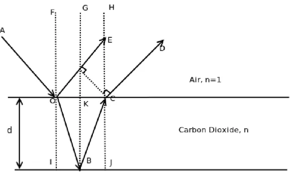
Figure 2-2: Schematic of the light scattering model.The dashed lines are normals to all the interfaces.
In the figure, the dent light beam AO hits the CO2 deposit surface at point O.
Part of it is reflected as OE according to the law of reflection such that θ1 =6 AOF = 6 F OE. The other part is transmitted through the CO
2-vacuum/air interface as OB.
The transmission follows the Snell’s law such that
nairsinθ1 = nCO2sinθ2 (2.1)
where θ2 =6 IOB, nair= 1 is the vacuum atmosphere’s refractive index, and nCO2 is
the carbon dioxide deposit’s yet unknown refractive index. The index of air will be dropped in the following derivations and n shall refer to the refractive index of just CO2. OB is then reflected from the CO2-substrate interface according to the law of
reflection as BC, and transmitted out as CD following Snell’s Law again such that θ3 =6 ECD = θ1. Of course part of BC can be reflectd at the air-CO2 interface back
into the cryodeposits, but we limit our derivation to only the first order reflection here.
Because the incident light beams AO and OB both experiences an 180-degrees phase shift at point O and B, respectively, then the conditions for OE and CD to constructively interfere is
lOD − nlOBC = mλ (2.2)
where m is any integer, lOD represents the length of OD, and n represents the
refrac-tive index of carbon dioxide, since nair = 1.
By inspection, we also have
cosθ2 = 2d lOBC (2.3) and, sinθ3 = lOE lOC = lOD 2dtanθ2 (2.4) finally, with the help of Snell’s law:
nsinθ2 = sinθ1 = sinθ3 (2.5)
we derive the following relationship between the thickness of carbon dioxide layer, its refractive index, and the incidence angle:
d = mλ 2n q 1 −sin2θ1 n2 (2.6)
This means the signal from a photodetector receiving the reflected light from the resist surface will fluctuate, and reaches local maximums every time the resist grows a thickness of d. Thus with two light sources hitting the surface with two different incidence angles, we get the following system of equations:
d1 = mλ 2n q 1 − sinn22α (2.7a) d2 = mλ 2n q 1 − sinn22β (2.7b)
where d1, α and d2, β are the thicknesses required for peaks and incidence angles for
the different light sources, respectively.
The increase in resist thickness by d1 or d2 is related to the deposition rate dddt and
elapsed deposition time ∆t by
d1 =
dd
dt · ∆t (2.8)
Equating this with 2.7, we have: dd dt · ∆t = λ 2n q 1 −sinn22θ (2.9)
where θ is either α or β. If we control the deposition rate dddt to be constant, then we can solve for both the refractive index and the deposition rate with the following:
n2 = sin2β − ∆tα ∆tβ 2 sin2α 1 − ∆tα ∆tβ 2 (2.10a) dd dt = 1 ∆tα · λ 2n q 1 − sinn22α (2.10b) = 1 ∆tβ · λ 2n q 1 −sinn22β (2.10c)
where ∆tα and ∆tβ correspond to the measured time between the photodetector
signal peaks for the two different incidence angles during deposition.
Once the deposition rate, which needs to be constant throughout a deposition, is obtained, it can then be used to calculate the total thickness of the resist layer. [15][8]. A constant period is a hallmark of constant deposition rate. An example of the dual laser interference signals is shown in Fig 2-3.
Finally, as shown by [5], picking incidence angles such that α − β is as big as possible minimizes the effect of mechanical/environmental noise has on the deposition rate and refractive index measurements. The incidence angles in the experiments are picked with this principle in mind.
Figure 2-3: An example of dual laser interference signals. The red and blue waveforms represent the fluctuating photodetector signals from two laser beams of different in-cidence angles. Note the difference in periods of the two waveforms, as well as the roughly constant peroid length within a waveform that is the hallmark of constant deposition rate.
2.3
Quartz Crystal Microbalance (QCMB)
Quartz is one member of a family of crystals that experience the piezoelectric ef-fect. Applying alternating current to the quartz crystal will induce oscillations. This property can then be exploited to make highly stable oscillators from quartz crystals. The frequency of the quartz crystal resonators is inversely proportional to mass. This relationship is summarized by the Sauerbrey’s equation[9]:
∆f = −2∆mf 2 0 A√ρqµq = − 2f 2 0 A√ρqµq ∆m (2.11) , where
• f0 is the resonance frequency of the oscillator’s quartz crystal. It is 6M Hz for
Figure 2-4: Quartz crystal as used for QCMB in the experiments. The gray circular quartz crystals are coated with gold electrodes by vapor deposition. When used in a QCMB, the active area is only the circular part in the center of the front electrode (left: back electrode, right: front electrode).
• ∆f is the frequency change.
• A is the piezoelectrically active crystal area. In the picture shown above of the typical crystal resonator, it is the area of the center circle of the front electrode. The active area is roughly equal 0.3177cm2 for the resonators ued in this work.
• ρq is the density of quartz (2.648g/cm3).
• µq is the shear modulus for the crystal (2.947e11g/cm · s2).
In applications, the quartz crystal resonator is usually housed within a sensor pack-age containing the osciallator driving electronics as well as frequency sensing circuits (QCMB refers to the housing in combination with the coated crystal). The crystal monitor housing often comes as part of a vacuum chamber feedthrough, allowing easy installation and interface with monitoring software.
Figure 2-5: Typical crystal monitor feedthrough package. The steel tubes provide cooling for the electronics, passing through the steel vacuum flange on the left. The square blocks on the right end contains the driving and sensing electronics, as well as the quartz crystal (the round golden circle)
Chapter 3
Experimental Setup and
Procedures
3.1
Experimental Setup
This section describes the experimental setup of the double laser interferometry sys-tem, as well as the design and modifications of the vacuum chamber started in [6]. A functional schematic of the entire system is shown in Figure 3-1.
3.1.1
Vacuum Chamber
Since the dry lithography process needs to be able to thermally evaporate and deposit organics and metals, a vacuum chamber with thermal sources is integrated with a glovebox filled with N2 gas. The only way to access the chamber interiors is through
the glovebox, this prevents unwanted moisture and oxygen from entering the chamber, as they can react with organic semiconductor materials and contaminate the carbon dioxide resist layer.
The vacuum chamber is made of stainless steel. Stainless steel was chosen because of its low degas rate which aids in high vacuum operations (pressure around 10−7torr). The chamber was machined by MIT Machine shop. The glovebox was constructed by and purchased from LC Tech Inc [6]. A 3D schematic of the integrated system
Figure 3-1: Functional schematic of the entire system: The box represents the vacuum chamber and any components inside or within the 6 planes of the box represent the components either within the chamber, or interfaced with the chamber walls (such as flanges). Green lines represent liquid nitrogen (LN2) flow along the arrows’ directions. Red lines represent electrical connections and the signals flow in the arrows’ directions. Blue lines represent the optical signals. Gray lines represent the flow of gas, which follows the direction of the arrows nominally.
is shown in Figure 3-2. For dimensions of the chamber, see Figure A-1. Note that since the chamber is built for PVD purposes, the inside walls are lined with aluminum panels made of steelwire frames wrapped by UHV aluminum foils. The panels are attached to the walls mainly by the wireframes’ flexing outward.
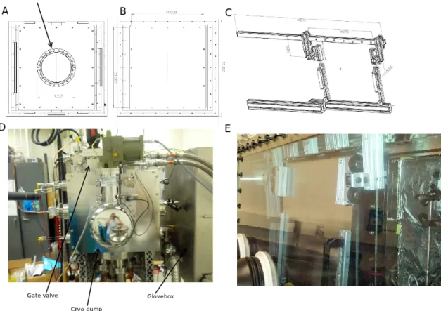
Figure 3-2: A: 3D cad drawing of the vacuum chamber mated with the glovebox. B: 3D cad drawing of the complete chamber. C: Photo of the front of the entire assembly.
Figure 3-4 to Figure 3-6 show the chamber construction in more details, along with the corresponding photos.
Figure 3-4: A: Cad drawing of the back panel of the chamber and the cryogenic pump placement. B: Front of the chamber without door handles. C: Front door sliding mechanism. D: Photo of the back of the chamber showing the gate valve and cryo pump placement. E: Photo of the sliding door inside the glovebox.
The vacuum in the chamber is achieved through the combined efforts of a rough pump and a cryogenic pump. A Busch Fossa scroll vacuum pump is used as the dry rough pump able to maintain the chamber at 10−3 torr. The pump accesses the chamber through the rough valve on the chamber’s left side. After reaching the low 10−2 torr, the rough valve is closed and rough pump turned off. The gate valve can then be opened to give the CTI-Cryogenics cryogenic pump access to the chamber. The cryogenic pump works by trapping gases by condensing them on a cold surface, achieving a pressure down to 10−8 torr. The gate valve is located on the back panel of the chamber (as shown in Figure 3-3 and 3-4), separating the cryopump (visible in
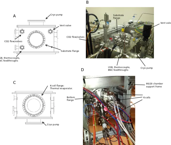
Figure 3-5: A: Cad drawing of the top of the chamber, showing locations of valves, flanges and feedthroughs. B: Photo of the top of the chamber. C: Cad drawing of the bottom of the chamber, showing locations of the K-cell flange. D: Photo of the bottom of the chamber.
Figure 3-6: A: Cad drawing of the left side of the chamber, showing locations of valves, flanges, and feedthroughs. B: Photo of the left side of the chamber. C: Cad drawing of the right side of the chamber, showing locations of valves, flanges, and feedthroughs. D: Photo of the right side of the chamber.
3-4) from the chamber interior. The sliding door is pushed against the front of the chamber by the pressure differential during vacuum. To gain access to the chamber interior, both the gate and rough valves are closed, and the vent valve (visible in Figure 3-5) is turned on, allowing the inert nitrogen gas from the glovebox to refill the chamber and increase its pressure.
A convectron gauge is used to measure pressure down to 10−3 torr while an ion-ization gauge is used for pressure below that. All the valves and gauges described in this section so far are intalled via a 2.500 flange/feedthrough.
The 1000 K-Cell flange is installed on the bottom of the chamber, through which the K-Cells and related wiring/cooling tubes are attached (Figure 3-5).
3.1.2
Chuck and Substrate Holder Design, and Substrate
Cooling
In past works studying dry ice, the low temperature needed for condensation was achieved either through using the cryopump surface as a substrate [8][5], or making more permanent substrate setups [16][13]. These approaches are not viable in a PVD setting because the substrate needs to be easily replaced as devices are made.
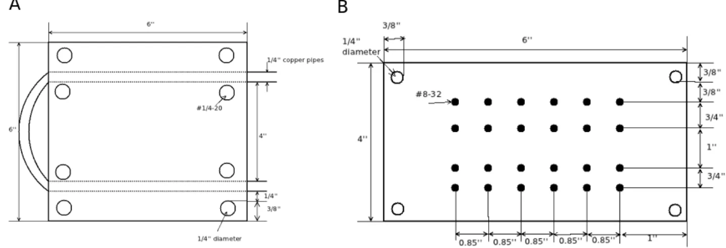
With this in mind, a chuck and a substrate holder were designed, a combination that is rather common in PVD chambers. The chuck is attached to the 1000 top flange of the chamber by nylon screws and nuts. Nylon screws and nuts are used to isolate the chuck thermally from the rest of the system. The substrate holder is attached to the chuck via steel 1/4 − 20 screws. Finally, the substrate, thermocouple, and crystal monitor can be mounted onto the substrate holder via 8 − 32 screws. See Figure 3-7 for schematics.
To bring the substrate down to a temperature low enough to condense CO2,
thermal conduction is critical. Both the chuck and substrate holder are machined out of Oxygen-free High Thermal Conductivity (OFHC) copper to maximize heat transfer. The cooling is done by flowing liquid nitrogen (LN2) at 77◦K through the chuck. Two 1/400 diameter holes are drilled through the 3/800 thick chuck lengthwise
Figure 3-7: A: Schematic for the chuck. B: Schematic for the substrate holder.
and brazed to copper tubes at the ends. The tubings are then connected via swageloks to the LN2 feedthrough (as shown in Figure 3-6). The inlet is supplied LN2 from a tank with pressure up to 5psi, and the LN2 exhaust pipe simply release the liquid into air.
To ensure the maximum thermal conduction, thermal contact is achieved through the following ways:
• Indium foils are placed in every interface as they are highly thermally conduc-tive and when pressure is applied, conform to the uneven surfaces that might otherwise become gaps of vacuum, which are superb thermal insulators. 23 of the substrate holder-chuck interface is covered by indium foils. All of the sub-strate mirror-holder interface as well as the crystal monitor-holder interface are covered by a piece of indium foil.
• The metal surfaces in contact are polished to achieve better thermal contact. • The inlet LN2 tubes are wrapped in insulation outside of the chamber to
mini-mize heating of LN2.
Further, since the goal of this work is to assess the quality of CO2 deposit
Figure 3-8: A: The chuck is attached onto the top of the chamber via nylon screws and nuts. The substrate holder is screwed onto the bottom of the chuck. LN2 flows through the insulated inlet (see Figure 3-6) to the feedthrough, into the chuck’s througholes via brazed copper tubes and out of the feedthrough again. The copper tubes are connected to the feedthrough and each other via swageloks. B: Looking up at the chuck-substrate-holder assembly. The substrate mirror is secured onto the holder via spring clips. The thermocouple is secured via screws. Two aluminum pieces across the top of the crystal monitor casing are screwed into the substrate holder, securing the housing and allowing it to be cooled.
properties as OLED display substrates. Indeed, the substrates used in the experi-ments are the same glass used in OLED fabrication but coated with 1nm of aluminum to have the appropriate thermal properties and the abilty to reflect light.
3.1.3
Optics
Since during the deposition process, the chamber pressure can reach 10−8 torr, it is unwise to place laser sources inside the chamber (even solid state diode lasers). Despite that approach’s ease of alignment, the vacuum causes the laser to overheat and the power output decays as a result (shown in Figure 3-9).
Figure 3-9: The power output of a 1mW, 632nm Thorlabs CPS180 diode laser inside high vacuum over time as measured by a Newport-818 Photodetector interfaced with a Keithley 2600 source meter
Thus, the light source has to be provided from outside the chamber, and shined through the quartz window viewport on the side of the chamber (shown in Figure 3-6).Further, to minimize alignment complexity, a Radius 405-25 CDRH laser manu-factured by Coherent, Inc is used as the light source. The Raidus 405-25 is a 405nm, thermal-electrically cooled laser with 25mW output, providing plenty of power to be split even after multiple bounces. Further, a stable source signal is important in detecting the expected oscillations.
As the chamber is mated with the glovebox, pressure changes and mechanical vibrations within the glovebox can result in shift of laser beam paths and noisy signals if the optics are not properly mounted.
The laser is mounted on a separate optical table, along with the chopper (described in the instrumentation section), below the glovebox. Its beam is reflected vertically through the gap between the backs of the vacuum chamber and the glovebox, reaching the viewport (shown in Figure 3-10). The separate optical table provides stability and mechanical isolation for the laser source.
Figure 3-10: Photos showing the laser setup, the blue arrows show the laser beam’s direction. A: The 408nm laser, chopper, and a 45◦ mirror are mounted on an optical table below the glovebox/chamber to provide stability. B: The laser table setup seen from the back of the chamber assembly.
The vertical beam is then reflected through the quartz window by a mirror mounted onto the flange itself as shown in Figure 3-11. It is of note that the mirror was first mounted in front of the quartz window by compression: bases at the two ends of a rod on which the mirror is mounted press against the sides of the chamber and the glovebox, with friction supporting the setup. While secure and simple, the mirror in this setup is easily shifted by changing pressure of the glovebox, changing the beam
path through the viewport.
Inside the chamber, a 50-50 beamsplitter is mounted in front of the viewport at the left wall of the chamber, directing one beam toward the right and the other toward the front. The front beam is intercepted and reflected vertically up to a second mirror, which then reflects the beam toward the substrate. The right beam is reflected by a mirror close to the center of the chamber toward the substrate. In this configuration, the front beam always hits the substrate with incidence angle α > 45◦ while the right beam hits the substrate with angle β < 45◦. This helps to maximize incidence angle separation during alignment and provides more robustness for the measurements (see the previous chapter).
Two Newport-818 silicon (400-1100nm) photodetectors are mounted toward the right of the chamber, receiving the reflections from the substrate.
To provide stability from mechanical noises, all the optical equipments inside the chamber are fixed onto optical breadboards. See Figure 3-12.
3.1.4
Gas Addition
According to [6], the CO2 addition was initially going to be controlled by the
MKS-2179A Massflo Controller coupled with the MKS-246 Power Supply/Readout. How-ever, the smallest flow rate possible for that setup is 0.2sccm, which makes the depo-sition rate too fast to be observed.
Instead, CO2 gas is leaked into the chamber by an LVM940 Variable Leak Valve
(by Kurt J. Lesker Company), coupled to a stop-valve which connects to a research grade carbon dioxide tank fitted with a VWR CO2 regulator. The variable leak valve
is continuously controllable between 10−3 and 10−11 mbar · l/s. It is actuated by a control knob with 10 continuous turns, and each turn is divided into 5 major markings. Since no data is available relating leak rate to number of turns, we have adopted the knob’s markings as a measure of leak’s size, which is then later correlated with the resulting chamber pressure in subsequent experiments (see experimental procedure section).
Figure 3-11: Photos showing the viewport setup, blue arrows indicate laser direction. A: The laser is directed vertically through the gap between the chamber and glovebox. B: The mirror setup is clamped onto the viewport flange by tightening aluminum tabs along a threaded rod. C: The mirror is able to slide parallel of the viewport and rotate around the rod to adjust reflection angle.
Figure 3-12: Photos showing the optics setup inside the chamber. A: The red and blue arrows originate from the beamsplitter. Red indicates the front beam hitting the substrate with α > 45◦ while blue indicates the right beam hitting the substrate with β < 45◦. The photodetectors are on the right side of the chamber with blue wires coming out. Note the optical breadboards. B: The beamsplitter is mounted right in front of the viewport. C: A closer view of the front beam optic setup. Also indicated is the camera perch (see the instrumentation section)
method connects a 1/400 copper tube to the leak valve inside the chamber and is di-rected at the substrate. Because of the low pressure, the gas molecules act ballistically and the deposition pattern becomes highly directional. Pointing the tube toward, but parallel to the substrate does not seem to yield deposition pattern differing from that of the second method. In the second method, no nozzle is used and the gas simply flows from the leak-valve opening. This is known as the back-fill method and is used in the final experiments.
Figure 3-13: The gas addition system. A: CO2 flows from the tank to the stop valve,
then through the variable leak valve. The support plate prevens the bending of the gas leak feedthrough. B: The first gas addition method used a nozzle connected to the leak opening, pointing toward the substrate.
3.1.5
Instrumentation
The two Newport-818 photodetectors come with BNC connectors. However, only the Bayonet-BNC CF Flange feedthroughs (by Kurt J. Lesker, part number IFTBG022033) were available at the time of experiments, thus the detector BNC connectors had to be modified. The BNC connectors were cut and the cables were stripped and separated into the signal wire (blue plastic wire), and ground wire (the metal sheath and the
clear plastic wire). The signal wires are connected to the bayonets via berylium butt splices, while the ground wires are screwed into a tapped hole on the feedthrough’s body via terminal connectors. This modified connection yields no signal integrity problem for the subsequent experiments.
As described in the optics section, a thermal-electrically cooled laser was used for its stable power output. To further eliminate and detect unwanted noise, the pho-todetectors are connected to two SR830 lockin amplifiers made by Stanford Research Systems. The operation of lockin amplification relies on the orthogonality of sinu-soidal functions. Specifically, when a sinusinu-soidal signal with frequency f1 is multiplied
by another sinusoid of frequency f2 6= f2 and integrated over a time much longer than
either signal’s frequency, the result is 0. In the case when f1 = f2, the result is equal
to half of the product of the amplitudes.
In practice, the chopper (shown in Figure 3-10) modulates the laser signal by blocking it with a reference frequency fr. This same reference signal is used by the
lockin amplifiers to multiply the photodetector signals. After integrating and low-pass filtering the product, only a DC signal that’s proportional to the chopped laser signal is left. The lockin amplifiers were sensitive enough to diagnose that the laser beam path shifts were caused by glovebox pressure changes.
The data acquisition software was written in labview to interface with the lockin amplifiers via GPIB. A screenshot of the labview program dashboard is shown in Figure 3-15. Throughout the experiments, the lockins were configured with 1µA signal limit, and low-pass filter time constant of 100ms with −24dB roll-off. The chopper frequency varied somewhat, but the specific frequency is not crucila as long as it’s not a multiple of 60Hz.
The temperature of the substrate holder is measured by an Omega thermocouple. The measuring end is secured onto the substrate holder via a screw (see Figure 3-8) while the cable ends are spliced and connected to a Fluke thermometer via a thermocouple feedthrough (see Figure 3-14).
The mass of the deposited CO2 is measured by a modified Inficon crystal monitor
Figure 3-14: The instrumention feedthroughs are connected to a single flange on top of the chamber.
the crystal monitor housing against it. Indium foil is sandwiched between the bottom of the housing and the holder to enable better cooling of the quartz crystal via LN2 flowing through the chuck. Unlike the usual crystal monitor assembly, which requires two cooling tube connections in addition to the BNC cable, only the micro-BNC is needed in this setup for signal acquisition. The cable connects via the QCMB feedthrough to an Inficon Qpod, which connects to PC via USB and displays data through the accompanying software. To run the software, a density needs to be entered for CO2 (which the software uses to derive thickness). However, since the
density is yet unknown, an arbitrary value is entered so the quartz frequency data can be recorded (tooling factor is kept at 1). Note that the qpod software requires disabling driver signature in Windows 7.
Finally, a Logitech HD Webcam C270 is used inside the chamber for alignment purposes as well as observing the substrate during deposition. The camera was choosen for its robustness in high vacuum. Its perch spot is indicated in Figure 3-12 and connects to PC via a USB feedthrough (see Figure 3-14).
Figure 3-15: Top: Screenshot of Labview program dashboard monitoring the outputs of the lockin amplifiers. Bottom: Screenshot of the qpod software with the graph plotting qpod frequency.
3.2
Experimental Procedures
3.2.1
Laser Alignment
Each experiment always starts with aligning the laser beams. To achieve the most noise-free measurements, the incidence angle separation needs to be maximized. Fur-ther, both beams are incident at the same spot in the center of the substrate mirror for more accurate thickness measurements. The incidence angles are calculated by cos−1(L/H), where H is the measured distance from the incident spot on the sub-strate to the photodetector, and L the vertical distance from the spot to the plane of photodetector parallel to the substrate. Because the distances are measured by hand
wih a tape measure, there’s always an uncertainty of 0.5cm, which is considered in the data treatment.
Despite the nitrogen environment and the high vacuum, there will always be mois-ture inside the chamber and deposited onto the substrate. As the chamber pressure lowers, the residual moisture is pulled away from the substrate surface and this affects the photodetector signals with the same Bragg interference principle. If aligned cor-rectly, upon pulling vacuum, the photodetector signals should increase as less deposit on the substrate means higher overall signal. Similarly, the photodetector signals would decrease slightly during substrate cooling depsite the lack of CO2 gas flow due
to the residual moisture condensation. In many experiments, the surface of the sub-strate was cleaned with Kim-wipes to facilitate alignment. However, this damaged the thinly coated substrate surface which had to be replaced.
To minimize moisture build up on the substrate, the chamber pressure should be in the 10−7 torr range before cooling down the substrate. Also, the substrate should be allowed to warm up in vacuum for as long as possible (to at least over 200◦K) before venting the chamber for access.
Figure 3-16: Results of venting the chamber while the substrate is still cold in regular atmosphere: the substrate is covered by water ice
3.2.2
Substrate Cooling
Substrate cooling is arguably the most crucial part of the experiment and cooling problems are also the hardest to diagnose. As the substrate is made of glass, the thermocouple cannot be easily mounted onto it to measure its temperature. Despite the various techniques employed to ensure optimal thermal contact, the substrate holder surface can only be cooled down to 98 − 100◦K range, compared to LN2’s 77◦K. An experiment was done using a 200 × 200 piece of aluminum (same size as
glass substrate) with mirror finish as the substrate. The thermocouple was mounted onto it and measured 102.5◦K at the lowest. Given that aluminum has much higher thermal conductivity than glass, it can be assumed that the glass substrate’s lowest temperature is greater than 102.5◦K. While reliable phase data of CO2 is not available
in regions of interest to this work, it’s reasonable to assume our experiments are operating on the edge of carbon dioxide gas-solid phase as a measured substrate holder temperature increase of even 1◦K can result in slower deposition rate (longer period between peaks in photodetector signals).
In the experiments, liquid nitrogen is pushed through the feedthrough into the chuck and back out. Fast cooling requires building up the pressure inside the LN2 tank by injecting N2 gas, see Figure 3-17.
3.2.3
Gas addition
Once the measured substrate holder temperature has reached its lowest around 100◦K, CO2 gas flow can start. The stop-valve is opened first, followed by the CO2 tank
reg-ulator. The regulator pressure is held at 0.5psi to provide enough line pressure. At this point, the chamber pressure is likely to rise about 10−8 torr. The stop valve is openned before the leak-valve because of the former’s tendency to trap air: if the stop-valve were openned after the leak-valve, its trapped air would cause a sudden pressure increase and result in a spike in CO2 deposition rate, which is not desirable
for controlled measurement.
The leak-valve, on the other hand, opens gradually and is less prone to a sudden burst of flow, As described previously, the valve’s knob markings were used as a measurement of leak size. A leak size of 26m (26/50 markings with 5 markings per turn of knob, and 10 turns available total) is required to detect any signal oscillations. Table 3.1 shows the observed relationship between knob turns and the resulting stable chamber pressure when the base pressure is at most 6 × 10⁻⁷ torr. Because one of the goals of this work is to find a fast deposition rate for the lithography process, most of the experiments done are with a chamber pressure of 10−3 torr or above.
Leak Valve Opening Chamber Pressure
26m 4.6 × 10⁻⁶ torr 26.25m 3.6 × 10⁻⁶ torr 26.5m 1.0 × 10⁻³ torr 26.6m 1.7 − 1.8 × 10⁻³ torr 26.7m 2.5 − 2.8 × 10⁻³ torr 26.75m 3.3 − 3.6 × 10⁻³ torr
Table 3.1: Leak Valve Opening vs. Chamber Pressure when the base pressure is less than 6 × 10⁻⁷ torr
Figure 3-18 shows a single photodetector signal with varying periods as a result of changing leak-rate/chamber pressure, thus changing CO2 deposition rate.
Eventually, the photodetector signals become too weak to distinguish oscillation features as a result of too much scattering by the carbon dioxide layer. The CO2
Figure 3-18: Photodetector signal showing varying periods as a result of varying leak-rate.
the gas flow. However, as the LN2 flow is turne off and the substrate temperature allowed to increase, the chamber pressure rises as the CO2 deposits sublime.
3.2.4
Data Collection
To obtain the most informative data, the qpod software and the lockin-monitoring labview program should start recording at the same time. This ensures the correct calculation of thickness and mass, and thus density of the deposits.
Further, the webcam also provides the most immediate feedback on the state of deposition, as shown in Figure 3-19.
Figure 3-19: Left: Webcam shot of the laser reflection off the substrate before de-position. Right: Laser reflection off the substrate during dede-position. The deposits make the reflection more diffuse, spreading across the entire substrate. This is a very useful tool in diagnosing deposition problems.
Chapter 4
Discussion
4.1
Experimental Data
Figure 4-1 shows the data obtained from a typical deposition. Notice that except for an increased period for just one cycle, both photodetector signals oscillate with roughly constant period, which indicates constant CO2 deposition rate. This constant
deposition rate is corroborated by the linearly decreasing crystal monitor frequency curve starting around 500s. The DC levels of the photodetector signals decrease with time beacuse as the resist layer gets thicker, less light is transmitted through the resist-air interface. Oscillation features typically become indistinguishable after a resist thickness of about 5µm.
Note that for both photodetector signals, the periods increase for one cycle, ac-companied by the flattening out of the QCMB’s frequency curve. This phenomenon is present in all the deposition data and is almost always accompanied by a momentary increase in chamber pressure. Furthermore, the slowdown happens after the same number of oscillations for all depositions. This observation seems to indicate that the deposition rate upon opening the leak-valve is largely constant, experiences a brief sudden slow down, and then goes back to the original rate. One possible explanation is that because the leak-valve is openned after the stop-valve, there is still some build-up of residual gas within it and at a particular pressure–indicated by the consistent timing of the slow-down, it is release as a burst into the chamber. The substrate
cannot cool down a sudden influx of mass fast enough, thus causing the deposition slow-down.
Figure 4-1: A typical deposition data. The red and blue curves are the photodetector signals. The green and magenta curves are the crystal monitor frequency change and its linear fitting, respectively.
While conducting data analysis, however, this abnormal period is ignored and ∆tα,
∆tβ in Eq 2.10 are calculated from averaging the rest of the periods from channel 1
and channel 2 waveforms, respectively. The instaneous change in frequency of the quartz crystal ∆f (see Eq 2.11) is taken to be the slope of the linear fitting of the quartz frequency curve after the slow down. Note that because of the decreasing DC levels of the photodetector signals, the local extrema from which the periods are calculated were picked out by hand.
Given the list of local extrema time positions and quartz frequency slope, Eq. 2.10 and Eq. 2.11 can be applied to find the density, refractive index, and deposition rate for the given trial (running the program analyze all.m in App B will display the results for all the depositions). Further, since the angle measurements were uncertain, the
same set of calculations were done three times for each trial: one for the measured angle values, one for angle values with the least separation, and one for the pair with the most separation. The angle values of the last two sets are calculated from applying the 0.5cm uncertainty to the incidence angle formula.
The photodetector and crystal monitor plots are shown in Figure A-2 through Figure A-10. Note that increasing lockin amplifers’ sampling rate makes more signal extrema distinguishable.
4.2
Results and Comparison
Figure 4-2 through Figure 4-5 show the relationship between the calculated CO2
density, crystal monitor frequency decrease, CO2refractive index, and CO2deposition
rate vs. the chamber pressure during depositions. The errorbar limits are the property values calculated from the different pairs of angles for a given deposition.
Figure 4-2: Pressure vs. Density
In Figure 4-2 and Figure 4-4, the linear fit is approximately of a constant value. They suggest CO2has a density of 1.5065±0.01g/cm3and refractive index of 1.5±0.01
under pressure between 10−3 and −4 × 10⁻³torr. The temperature of the substrate is unknown, but as described in the previous chapter, can be estimated to be 102 ± 2◦K.
Figure 4-3: Pressure vs. abs(Quartz Crystal Frequency Slope)
Figure 4-5: Pressure vs. Deposition rate
4.2.1
Refractive Index
CO2’s refractive index was shown by [15] to be roughly constant at 77◦K between
10−5 and 10 torr. While [8] has shown that the refractive index fluctuates with temperature under constant pressure, the paper seems to suggest in its conclusion that n is not affected much by pressure1. Further, our refractive index value fits well
with [15]’s extrapolation with respect to wavelength measured under 10−5 torr. Thus our result is likely a very good estimate.
4.2.2
Density
According to [8], CO2’s density changes from 0.98 to 1.5g/cm3 as temperature varies
from 10 to 86◦K, under 10−8 torr. The authors suggest that for deposition tempera-ture > 50◦K, the density stays approximately constant. Accordin to [15], the density of CO2 increase from about 1.3g/cm3 to 1.7g/cm3 as deposition pressure increases
1Satore et al. mentioned in the paper’s conclusion that their refractive value between 1.21 and
1.35 measured at 77◦K and 10−8torr ’compares well’ with Tempelmeyer’s refractive index between 1.38 and 1.42 measured at 77◦K and 10−5 to 10 torr[15], implying that pressure does not affect n very much
from 10−4 to 1 torr. Therefore, our fitted density of 1.5065 ± 0.01g/cm3 fit well
with both observations. The fact that our calculated density stays roughly constant does not contradict with [15]’s observation that density increases with the deposition pressure because of the small pressure range used in our experiments.
However, since the density is calculated from the thickness measured in the center of the substrate, and the mass is measured by the crystal monitor mounted to the side of the substrate, in the situation where the thicknesses at the two locations differ by a significant amount, the density value can be erroneous.
To obtain a more accurate density measurement, deposition uniformity would have to be checked across the substrate. A second way is to use the surface of the crystal monitor as the substrate2, but this introduces a lot more alignment complexity.
4.2.3
Deposition Rate and Crystal Quartz Frequency
Figure 4-3 shows the rate of the QCMB’s frequency decay is proportional to the deposition pressure.. Figure 4-5 shows the deposition rate is also proportional to the deposition pressure. These relationships make physical sense and confirm the correctness of our experiments. Further, the range of leak-rates explored yield a deposition rate suitable for high speed lithography processes. Namely, the deposition rate when the chamber pressure is between 3.3 − 3.6 × 10⁻³ torr/(26.75m leak rate) is approximately 11.5nm/s, which means it would take around 7 minutes to deposit 5µm of resist that is needed for the sublimable lithography process.
Even though the uniformity of the deposition cannot be confirmed, the highly linear dependence of both quantities on pressure suggest a strong correlation between the deposition trend on both the substrate and the crystal monitor. This can be exploited to derive a pseudo-density µ which allows the thickness of the deposit on the substrate to be calculated solely by the crystal monitor in this particular geometry. µ thus combines roles of both actual density and the geometric tooling factor for the crystal monitor. We derive µ for this particular geometry here.
From the linear fit in Figuqre 4-3 and Sauerbrey’s equation (Eq 2.11), we have:
∆f = −39835P + 9.6224 (4.1a)
= (−2.565 × 10⁸)∆m (4.1b)
where ∆f is the instantaneous rate of change in QCMB frequency at a given pressure in (Hz/s). ∆m is that of mass in (g/s). Rearranging:
∆m = ∆f
−2.5655 × 108 =
39834P − 9.6224
2.5655 × 10⁸ (4.2)
Therefore the instantaneous thickness growth rq in (cm/s) onto the crystal is, after
choosing P = 1 torr for convenience: rq = ∆m µ0A = 39824 Hz s µ081505935Hz·cm 2 g (4.3)
where A = 0.3177cm2 is the quartz crystal’s active area, and µ
0 is the true density
of the quartz deposit in (g/cm3). From the linear fit in Figure 4-2, and after picking
P = 1 torr we have the instantaneous growth rate rl in (m/s) of CO2 onto the
substrate as:
rl = (3.4302 × 10⁻⁶)P − 1.2145 × 10−9 = 3.4296 × 10⁻⁶ (4.4)
For the crystal monitor to correctly predict the growth rate on the substrate and pick out the pseudo-density µ, we require:
rl = rq (4.5a) 3.4296 × 10⁻⁶m/s = 3.4296 × 10⁻⁴cm/s = 39824 Hz s µ(81505935Hz·cmg 2) (4.5b) µ = 1.4247g/cm3 (4.5c)
4.3
For future use
In future depositions where the relative positions of the crystal monitor and the substrate stay largely the same (and the substrate holder temperature doesn’t deviate by more than 1 degree from the 98 − 100◦K range), only the crystal monitor with the newly derived µ-value as the density parameter is needed to measure the growth rate and thickness.
However, if the relative positions or the thermal conditions were to change, the crystal monitor will have to be recalibrated via the interferometry method to obtain a new pseudo-density.
Further, the combination of the interferometry method3 and QCMB can be used to characterize any thin film capable of forming a smooth surface for refractive index, density, thickness rate on the substrate and mass rate on the QCMB. The QCMB can subsequently be configured to measure thin film thickness in all future growths.
Chapter 5
Conclusion
CO2 has been shown as a suitable sublimable mask for organic semiconductor device
patterning. This work seeks to understand and control the CO2 deposition process in
a PVD context. Hardware was constructed to allow unobtrusive substrate cooling. By combining the optical technique of dual-laser interferometry to measure the deposition rate and refractive index, and the QCMB measuring the mass deposited, the CO2
layer’s density can be determined. Further, these properties were studied in a range of deposition pressures, finding leak rate and chamber conditions that can quickly and precisely form resist layers needed for OLED fabrication. Finally the techniques can be used to calibrate a QCMB as the only instrument needed to measure the growth of any transparent, smooth thin film.
However, the techniques have much room for improvement. Most importantly, the chuck and substrate holder can be re-designed to promote better thermal contact with each other and the substrate, as cooling is responsible for much of the problems encountered during this work. Better cooling would also largely prevent non-uniform deposition, whose effect is ignored in the data analysis. Even though [16] has shown that uniformity is not a problem in small area deposition, it must be investigated before any viable large area fabrication using the dry lithographic technique can happen. Further, the ability to cool down the substrate even more in a PVD setting would help to find conditions that would produce resist with the greatest density, which is desirable for lithographic purposes.
Appendix A
Figures
Figure A-1: Cad drawings showing the dimensions of the vacuum chamber, dimen-sions are in inches. A: Back panel and gate valve flange. B: Front door without door handles. C: Right panel and the flange placements. D: Top view of the inside the chamber.
Figure A-2: 7/23/2012 deposition
Figure A-4: 7/26/2012 deposition
Figure A-6: 7/30/2012 deposition 2
Figure A-8: 7/31/2012 deposition 2
![Figure 1-3: A micrograph of the 115µm-tall pillar SU-8 stamp (top) used to pattern circles of Alq 3 (bottom ) [1]](https://thumb-eu.123doks.com/thumbv2/123doknet/14753706.581411/22.918.182.732.194.426/figure-micrograph-tall-pillar-stamp-used-pattern-circles.webp)