Design of a Hermetically Sealed MEMS Resonator with Electrostatic
Actuation and Capacitive Third Harmonic Sensing
By
Eric B. Newton
B.S. Engineering Physics and Mathematics University of Wisconsin - Madison 2009
Submitted to the Department of Mechanical Engineering in Partial Fulfillment of the Requirements for the Degree of
Master of Science in Mechanical Engineering at the
MASSACHUSETTS INSTITUTE OF TECHNOLOGY
February 2012
@2012 Massachusetts Institute of Technology All rights reserved
MASSACHUSETTS INSTITUTE OF TECHNOLOY
FEB 16
2
L!BRARES
ARCKIES Signature of Author:Department of Mechanical Engineering
j
/
January 20, 2012 Certified by: Carol Livermore Visiting Scientist Tyip-upervisor Accepted by: David Hardt Professor of Mechanical Engineering Chairman, Committee for Graduate StudentsDesign of a Hermetically Sealed MEMS Resonator with Electrostatic
Actuation and Capacitive Third Harmonic Sensing
By Eric Newton
Submitted to the Department of Mechanical Engineering on January 20, 2012, in Partial Fulfillment of the Requirements for the Degree of Master of Science in
Mechanical Engineering ABSTRACT
A microscale beam resonator has been designed and fabricated for use as a modular pressure sensor for vacuum applications. The device dimensions have been optimized to provide
measurable signals with low noise. Electrostatic actuation and sensing are both performed using only one pair of electrodes. The motion of the cantilever changes the capacitance of the actuation electrodes at a frequency three times that of the actuation signal. This method allows the desired motion to be picked out using a lock-in amplifier with minimal interference from other unwanted signals such as parasitic leakage and noise. Unlike previous work, packaging and electrical contacts have been integrated into the fabrication to create a hermetically sealed device that can easily be incorporated into other MEMS designs.
Most resonators operate in vacuum because air damping at higher pressures greatly decreases both resonant frequency and quality factor. This loss is directly related to the pressure of the surrounding air, and therefore has been used in this design to measure the pressure. While the relationship is not linear, it is one-to-one. This means that once the device has been
characterized, pressure can be determined uniquely over a range from atmospheric pressure down to ~10- Torr.
The device was fabricated from two SOI wafers using standard wafer processing techniques. This means that unlike previous work, it can be readily integrated into other designs via wafer bonding. A single access port on the base provides a connection between the otherwise hermetically sealed sensor and other devices. To prevent squeeze film damping from limiting the motion of the beam, the cantilever tip has been perforated with an array of holes and a cavity was etched above where the cantilever will oscillate. Electrical contact can easily be made with the device as fabricated, so no additional packaging is necessary.
While the fabricated devices are hermetically sealed, resonance was never detected due to a combination of factors including: poor wafer bonding, parasitic leakage, a Schottky barrier at one terminal and a design error that led to an unexpectedly high frequency and quality factor. Modifications to the current design are proposed that should eliminate these problems in the next iteration.
Thesis Supervisor: Carol Livermore Title: Visiting Scientist
Acknowledgements
I feel quite lucky to have had such a gratifying Master's experience. Throughout the last two and a half years, I have been surrounded by people who were both very knowledgeable and happy to offer their advice on all sorts of questions. I would like to thank them for their support - I would not have finished without their help.
First and foremost, I would like to thank my adviser, Professor Carol Livermore, who has been a great mentor and friend. She has provided me with constant support and guidance from the moment I stepped onto campus. Her cheerful demeanor made our weekly meetings a
pleasure, and she was always happy to discuss my problems in my research, both large and small. I would also like to thank my new adviser Professor Martin Schmidt for taking me into
his research group for my PhD and offering sage advice to help me finish this project.
I would also like to thank all of my labmates for their friendship and support throughout the last two years. Aalap, Feras, Frances, Gunjan, Lei and Nader: you have always been willing to listen to me vent frustrations with research and life, and I have greatly enjoyed our many
birthdays, group dinners and especially the trip to Acadia. Thank you Feras and Lei for your advice on microfabrication. And a particularly large thank you to Aalap, who collaborated with me on the micropump project, for our long discussions about both of our projects.
I also thank Professor Tayo Akinwande, Dr. Hanqing Li and Dr. Luis Velasquez-Garcia and the rest of the micropump team. They provided advice and technical help throughout the
design, fabrication, and testing process. I also want to thank the MTL staff for training in the clean room. I am particularly thankful to Dennis Ward and Bernard Alemariu, who gave crucial insight into my fabrication process and helped troubleshoot problems when processing did not go as planned. I would like to thank Dr. Nicki Watson and the Whitehead Institute for allowing me to use their Critical Point Drier. My devices could not have been fabricated without her help. The project was financially supported by Professor Livermore, the Mechanical
Engineering Department of MIT (through a one year Presidential Fellowship) and DARPA. Finally, I'd like to acknowledge my parents, sister brother and girlfriend Rocio for the continuous moral support they have provided me with throughout this process. I always look forward to talking with and seeing you guys, and I could not have made it through these last two years without you all.
Table of Contents
List of Figures ... 9
List of Notation ... 14
1 Introduction ... 18
1.1 M otivation for Pressure Sensor ... 18
1.2 Review of Pressure Sensing with M EM S Resonators ... 19
1.3 Proposed Design... 21
1.4 Outline of Thesis... 22
2 Operation Principle - How Quality Factor Relates to Dam ping ... 23
2.1 Pressure Dependence Predictions ... 23
2.1.1 Clam ping and support losses ... 23
2.1.2 Bulk Dissipation... 24
2.1.3 Surface Losses ... 24
2.1.4 Therm oelastic Dissipation... 24
2.1.5 Fluid Dam ping Losses... 24
2.2 Dam ping on a cantilever beam ... 27
2.2.1 Drag... 27
2.2.2 Squeeze Film Dam ping ... 28
3 Design and Optim ization ... 32
3.1 Assessm ent of Actuation M ethods ... 32
3.1.1 Therm al, M agnetic and Piezoelectric Actuation... 32
3.1.2 Electrostatic Actuation ... 33
3.1.3 Beam Bending ... 37
3.1.4 Further analysis of the capacitive design ... 44
3.2 Analysis of Sensing M ethods... 47
3.2.1 Optical ... 47
3.2.2 Piezoresistive ... 47
3.2.3 Capacitive ... 54
3.3 Lim its on Dim ensions ... 59
3.3.1 Fabrication lim itations ... 59 6
3.3.2 Gravitation Effects ... 60 3.3.3 Frequency of Operation ... 61 3.4 M ATLAB optimization ... 63 4 Fabrication... 65 4.1 Overview ... 65 4.2 Die Layout... 66
4.3 Alignm ent M arks... 69
4.4 Bottom Layer ... 74
4.5 Top Layer.. ... 79
4.6 W afer Bonding... 84
4.7 Bonded W afer Processing and Release... 87
5 Testing ... 93
5.1 Test Setup .. ... 93
5.2 Results ... 98
5.2.1 Leak Testing ... 98
5.2.2 Electrical Testing... 100
5.3 Problem s with Current Design ... 103
5.3.1 Release Etch Undercut and Shorting... 103
5.3.2 Quality Factor... 106
5.3.3 Parasitic Capacitance ... 108
5.3.4 Rectified Signal ... 112
5.3.5 Sum m ary of Device Flaws ... 125
6 Future W ork ... 126
6.1 Im proved Bonding ... 126
6.1.1 How to im prove bonding ... 126
6.2 M etal Contacts... 127
6.3 Better isolation... 128
6.3.1 Decrease the area of parasitic capacitors... 128
6.5 Sum m ary of changes... 136 Appendix A: Stationary Beam Bending Solution ... 141 Appendix B: Fabrication Process... 142
List of Figures
Figure 2-1 Pressure dependence of Quality Factor. Blue indicates the viscous regime, green is the free molecular regime and at low pressures, red indicates that intrinsic effects (clamping, volume, surface, TED, etc) dominate pressure loss. The transition between viscous and molecular damping has not been shown, though a smooth transition between 1 Torr and 101
To rr s expecte . ... ... ---... . . . ... 26
Figure 2-2 - Visualization of the disk approximation for a vibrating cantilever beam. ... 27
Figure 2-3 - Approximation of a perforated plate with annular cells... 29
Figure 3-1 - (top) The nonlinear nature of electrostatic actuation can be seen in the first plot. Pull-in occurs at 14.65V, and can be seen in the first plot as the point where the gap goes to 0. (bottom) Spring softening caused by the decrease in the overall spring coefficient. Results are shown for an 1100pm x 220pm x 15pm silicon beam with a 2.5pm gap. ... 35
Figure 3-2 - Magnitude of resonance for several different levels of damping... 38
Figure 3-3 - Phase response for several levels of damping ... 39
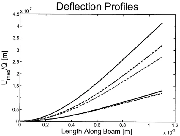
Figure 3-4 - Deflection of cantilever beams under various loading conditions for a 1100 pm x 220 pm x 15 pm beam actuated by a voltage of 14V. Solid lines are solutions to the Euler-Bernoulli equation; dashed lines are static solutions using basic beam theory with a constant force (no gap dependence). Blue indicates a point load at the end, red is the realistic situation with a distributed load over the actuation region, and black is a fully distributed load. The total force applied is the same across all loading conditions, so the distributed load for the black curves w as 1/L tim es the actual distribution. ... 44
Figure 3-5: Unbalanced actuation forces caused by misalignment are shown in red. Doped regions are shown in orange, undoped silicon in gray. ... 45
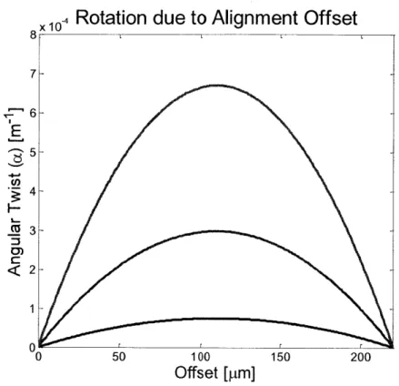
Figure 3-6 - Angular twist for 5V (blue), 10V (green) and 15 V (red) with a 15pm thick, 220pm w id e b e a m ... 4 6 Fig u re 3 -7 ... ... . . ... 5 2 Figure 3-8 Schematic of resonator, showing critical dimensions (Note: not to scale)... 60
Figure 4-1 - Schematic of fabricated device with wafers separated to show interior features. Yellow indicates highly doped silicon. ... 65
Figure 4-2 - Four quadrants each with a different hole diameters: 8pm holes (red), 6pm holes (orange), 4pm holes (green) and no holes (blue). ... 68
Figure 4-3 -Cantilever length of each die in the upper right quadrant. ... 69
Figure 4-4 - Process Flow for creating alignment marks ... 70
Figure 4-5 - M ask "D icing" ... . 71
Figure 4-6 - M ask "Resonator Alignm ent" ... 72
Figure 4-7 - A lignm ent M arks ... 73
Figure 4-8 - Detailed view of alignm ent m arks... 73
Figure 4-10 - M ask "Cantilever_ Electrode" ... 76
Figure 4-11 - Die level view of mask "CantileverElectrodes" ... 76
Figure 4-12 - Window used to align masks with alignment marks. The cross lines up with the alignment marks on the wafer, and the window allows for a wider field of view... 77
Figure 4-13 - Detailed view of alignment features from previous figure... 77
Figure 4-14 - M ask "Cant Plus_ Holes" ... 78
Figure 4-15 - Zoomed view of 750p.m long cantilever in "CantPlusHoles" mask ... 78
Figure 4-16 - Top layer fabrication process ... 80
Figure 4-17 - M ask "Second_Electrode"... 81
Figure 4-18 - Die level view of mask "Second_Electrode"... 82
Figure 4-19 - "N ested" m ask ... 82
Figure 4-20 - Die level view of m ask "Nested" ... 83
Figure 4-21 - "Cavity" m ask... 83
Figure 4-22 - Necessary anneal times based on furnace temperature. These values were scaled assuming that 21.5 hours produces a complete bond at 700*C [33]. ... 85
Figure 4-23 - Cartoon showing alignment for fusion bond... 85
Figure 4-24 - This image shows two wafers after bonding under the infrared camera. The white spot in the middle is the bulb of the light used to illuminate the wafers. The outer black ring is the extent of the wafer, though only a smaller (approximately 4 inch) disc can be seen through the hole in the support. The wafers bonded in the center leaving an approximately 1cm unbonded ring around the edge (shown by the fringes circled in red)... 86
Figure 4-25 - Post-bond processing ... 88
Figure 4-26 - M ask "V ia " ... . 89
Figure 4-27 - Die level view of "Via" m ask ... 89
Figure 4-28 - M ask "Expose Electrodes"... 90
Figure 4-29 - Die level view of mask "Expose_Electrodes"... 90
Figure 4-30 - Before and after release of cantilevers. The oxide layer can readily be seen in the left image, with residual stress causing a periodic rippling... 91
Figure 4-31 - Top and bottom views of a microfabricated device... 92
Figure 5-1 - Testing block diagram ... 93
Figure 5-2 - Diagrams showing aluminum base for test jig, a top view on top and a side view on bottom . Dim ensions are given in inches... 95
Figure 5-3 - Diagrams showing acrylic test jig cap, with a top view on top and a side view on bottom . Dim ensions are given in inches... 96
Figure 5-4 - Schematic showing placement of pogo pins in test jig. ... 97 Figure 5-5 -A cartoon cross-section of the device and electrical connections, highlighting the intended current path. Wires attached with conductive epoxy to pogo pins allow electrical co ntact w ith the d evice . ... 9 7
Figure 5-6 - Wires attached to pogo pins with conductive silver epoxy and taped to acrylic cap to p ro vid e stability ... 98
Figure 5-7 - Plot showing leakage around blank die ... 99 Figure 5-8 - Plot showing leakage through two test dies. ... 99 Figure 5-9 - Typical response before shorting was removed at the edges. Applied voltage was 5V rm s, 20dB gain, 500kQ m easurem ent resistor... 101 Figure 5-10 - A typical frequency sweep measurement from the lock-in after removing shorting with tape. Applied voltages were 2V-rms with a 3V DC offset, 500k measurement resistor,
20dB gain. Measurements were taken for 10s at each frequency, with 5Hz per step. While there are several peaks, none of them are repeatable, nor are they large enough to constitute
re so n a n ce ... 10 2 Figure 5-11 - Optical microscope picture showing top side of device. On the left side the lower wafer is exposed. In the bottom right the cap can be seen. The device layer (upper right) is visibly collapsed, creating a resistive short between the wafers. ... 103
Figure 5-12 - Some devices still had portions of the device layer that had collapsed (top left). However, many more were peeling (top right). The peeling was not uniform (bottom left) and in some places had completely separated from the oxide (bottom right). ... 105 Figure 5-13 - After using tape to remove the overhanging silicon. The edge of the remaining device layer can be seen outlined by the exposed oxide (purple). ... 105
Figure 5-14 - Relationship between pressure and peak width... 108 Figure 5-15 - An approximate circuit model for the actual device. The idealized case ignores Zp because it was assumed that the only relevant path was the intended one. However, the high impedance of the capacitive actuation gap makes several parasitic paths contribute significant third harm onic com ponents to the output signal . ... 109
Figure 5-16 - Intended path for current, with circuit elements superimposed over device cartoon. The impedance of the actuation capacitor at the resonator tip dominates over the
resistance of the doped leads... 109 Figure 5-17 - Parasitic path over the top of the resonator cap. It was assumed that the cap is approximately square, so the resistance is simply resistivity/thickness of the cap... 110
Figure 5-18 - Top and side views of device showing a parasitic leak path around the cantilever through the bulk silicon. The green shaded region shows the estimated area for the capacitive
path around the access hole... 110 Figure 5-19 - Circuit model for "real" device. The Rres, Cres path is the intended path
containing the resonator. All the others are parasitic impedances in parallel. ... 111 Figure 5-20 - Plots showing the relative impedance of the parasitic paths and the intended re so n ato r p ath ... 1 1 1
Figure 5-21 - Voltage across elements in testing circuit. The curves were measured separately (starting at different points in the waveform) and superposed on the same plot, so they don't
line up. It can be seen that the maximum of the resistor voltage and device voltage add up to the applied voltage from the lock-in amplifier, so this strange behavior is still obeying
K irch h off's law s... 1 12 Figure 5-22 - Plots of voltage across the circuit elements under positive and negative bias. .. 113 Figure 5-23 - Dopants implantation profile from Innovion. It should be noted that the substrate was actually P doped, so the green N dopants baseline should be P Dopants... 114 Figure 5-24 - Approximate doping profiles at 10500C and 11000C for several diffusion times: 1 hour (blue), 1.5 (actual time, black dashed line), 2hours (green), 4 hours (red), and 8 hours (te al)... 1 1 5
Figure 5-25 - Cartoon showing doping gradients. The bottom wafer was doped from the top, so the highly doped silicon is in contact with the pogo pin. The bottom wafer is upside down, so the highly doped region is on the bottom side. ... 116
Figure 5-26- Comparison of the first three harmonics of the lock-in amplifier actuation voltage. The frequencies shown are always the first harmonic frequency, so the actual second harmonic frequency is twice that shown on the axis. There is a change in the way the signal is created at 20.4kHz that is visible by a drop in the second harmonic and a rise in the third... 120
Figure 5-27 - The scaling function is shown here for a total voltage of 15V (almost pull-in). Dotted lines corresponds to the second harmonic, solid lines are the third harmonic. The black lines are the lower bounds where displacement was determined with a distributed actuation force along the entire beam. The blue lines are the upper bound where the entire actuation force on the capacitor is concentrated at the tip of the beam. The red lines in the middle show the actual situation where the beam is actuated over length I at the tip. ... 122
Figure 5-28 - Parasitic currents (shown in red) compared with the first harmonic current (black) thro ugh the reso nato r. ... 123
Figure 5-29 - Actual second and third harmonic current (shown in black) compared to the corresponding parasitic current (blue) for VAC = 7.5V... 124 Figure 6-1 -The old design is shown on the top with a 2mm cap ring and 1mm wide electrodes. The suggested design with improved isolation is shown below with a 0.5mm cap ring, 0.2mm electrodes, and an isolation trench through both device layers surrounding electrodes and cap.
... 1 2 9
Figure 6-2 - Relationship between actuation length and thickness for select voltages between 1 a n d 5 V (rm s)... 1 3 2
Figure 6-3 - Relationship between pressure and peak width for new design...134 Figure 6-4 - Deflection of cantilever beams under various loading conditions. Solid lines are solutions to the Euler-Bernoulli equation, dashed lines are static solutions using basic beam theory with a constant force (no voltage dependence). Blue indicates a point load at the end, red is the realistic situation with a distributed load over the actuation region, and black is a fully
distributed load. The total force applied is the same across all loading conditions, so the
distributed load for the black curves was 1/L times the actual distribution ... 135 Figure 0-1 Visualization of superposition used to determine beam deflection... 141
List of Notation
Q Quality Factor [-]
Us Energy stored per cycle [J]
Ud Energy Dissipated per cycle [J]
Oo 0Angular frequency or resonator[rad/s]
Qciamp Quality factor due to clamping and support losses [-]
yn Constant of proportionality in Qciampfor nth mode of vibration [-]
L Length of cantilever beam [m]
t Thickness of cantilever beam [m]
E Young's modulus [Pa]
E1 Elastic modulus [Pa]
E2 Loss modulus [Pa]
QVo1
Volumetric quality factor [-] Qsurface Surface quality factor [-]w Width of cantilever beam [m]
S Thickness of surface layer for Qsurf ace [ml
Eis Elastic Modulus for Qsurface[Pal E2s Loss Modulus for Qsurf ace [Pa]
QTED Thermoelastic Dissipation Quality Factor [-]
Constant used in QTED
[-C, Specific heat of silicon at constant pressure [J/K]
p Density of silicon [kg/m3]
T Temperature [K]
aT Coefficient of thermal expansion [m/K] ksi Thermal conductivity of silicon [W\(m-K)]
Kn Knudsen number [-]
A Mean free path [m]
Lc Characteristic Length [m]
kB Boltzmann Constant [J/K]
d Diameter of molecules [m]
p Pressure [Pa]
Qp,viscous Pressure quality factor for viscous regime [-]
y Dynamic viscosity [Pa-s]
M Molar mass of gas surrounding beam [kg/mol]
R Ideal Gas constant [J/(mol-K)]
Qtotal Sum of all quality factors [-]
Fdamping Damping force [NI
c Coefficient of damping [N-s/m]
V Velocity [m/s]
Fsphere Damping force on a sphere [N]
Fdish Damping force on a dish [N]
r Radius [m]
Cbeam Damping coefficient of beam [N-s/m]
V Volume [iM3
]
Pa Atmospheric pressure [Pa]
a Radius of cells in perforated plate [m] b Radius of holes in perforated plate [m]
g Current gap between cantilever and base electrode [m] Ae Area of annular region in each cell of perforated plate [M2]
#
Ratio of b/a [-]N Number of holes in perforated plate [-]
Csqfilm Squeeze film damping of perforated plate [N-s/m]
(g Function of
#
used in calculation of Csqfilm[-Fe Electrostatic force [NJ
EO Permittivity of free space [F/m] A Area of actuation for cantilever [M2]
V Actuation voltage [V]
g Current gap [m]
Ue Electric potential energy [J] k Cantilever spring stiffness [N/mi
ksystem Stiffness of entire system [N/mi
x Displacement[m]
y Damping factor [1/s]
FO Magnitude of oscillatory force [N]
AO Magnitude of oscillatory acceleration [m/s 2
E2 Angular frequency of oscillatory force [rad/s]
m Mass [kg]
xs Specific solution to displacement differential equation [m]
X0 Magnitude of forced displacement [m]
0 Phase of forced oscillation
Xniax Maximum forced displacement (at resonance) [m]
[rad/s]
u Beam displacement [m]
I Second moment of inertia [M 4
]
Fe' Electric force per unit length [N/m]
Gn.x)
Spatial dependence of the nth mode of vibration [m]7n7t) WTime dependence of the nth mode of vibration [s]
am Normalization constant for mth mode of vibration [-] 6
Smn Kronecker delta [-]
Kn Eigenvalues for the nth spatial mode of vibration [-]
mn Modal mass for the nth mode of vibration [kg]
cn Modal damping for the nth mode of vibration [N-s/m] kn Modal stiffness for the nth mode of vibration [N/m] gn Modal force for the nth mode of vibration [N]
1 Actuation length [m]
6(x) Dirac delta function [-]
VA C Magnitude of actuation voltage [V]
Umax Maximum beam displacement [m]
a Angle of twist per unit length [rad/m]
T Net torque on beam [N-m]
G Shear Modulus [Pa]
R Resistance [0]
v Poisson Ratio [-]
Pij Resistivity tensor [0-m]
it Current density in the i direction [A/m 2]
p Resistivity tensor of unstressed material [0-mi
7Tijkl Piezoresistivity tensor [0-m/Pa]
Ykl Stress tensor [Pa]
KIT Lateral piezoresistive coefficient [1/Pa] Et Transverse piezoresistive coefficient [1/Pa]
a, Lateral stress [Pa]
at Transverse stress [Pal
M Bending moment in cantilever [N-mI
y Perpendicular distance from neutral axis [m]
Rsquare Resistance for a square of material [0]
R' Total resistance over doped region of piezoresistor [0] Rfath Integrated resistance of one path of piezoresistor [0]
Wpath Width of piezoresistor path [0]
X1 Starting x value for resistive path [m]
X2 Ending x value for resistive path [m] Y1 Starting y value for resistive path [m]
Y2 Ending y value for resistive path [m]
Rlead Approximate resistance of one path [0]
Risolation Isolation between neighboring leads [Q]
C Capacitance [F]
Qe Charge [C]
i(t) Current [A]
i3(t) Third harmonic current [A]
CO Un-actuated capacitance of cantilever [F] un Beam deflection due to damping noise [m] C' Capacitance with damping noise variations [F]
Vn Johnson noise [V]
i' Current with Johnson noise contribution [A]
Ug Displacement due to gravity [m]
ag Gravitational acceleration [m/s2]
Fgrav Gravitational force on beam per unit length [N/m]
a Squeeze number [-]
Wmax Maximum allowable resonance frequency [rad/s] R1 Resistance of first electrode [0]
R2 Resistance of second electrode [0] Z'res Impedance of resonator path [0] Ry1 Resistance of first electrode [C]
Cpi First parasitic capacitance [F] Cp2 Second parasitic capacitance [F} Cp3 Third parasitic capacitance [F}
Zover Impedance of parasitic path over top through the cap [0] Rp2 Second parasitic resistance [0]
Cy4 Fourth parasitic capacitance [0]
Zaround Impedance of parasitic path around via through device layer [0]
cps Fifth parasitic capacitance [F]
Zunder Impedance of parasitic path around via through bulk silicon [0]
i2(t) Second Harmonic Current [A]
f3(VAC) Scaling function for the third harmonic for biased actuation [-]I
1 Introduction
Interest in Micro Electromechanical Systems (MEMS) has been growing, with increasing applications for MEMS accelerometers, strain gauges, and microphones. At the interface with biology, BioMEMS have been able to make their way into medical applications from as basic as biochemical sensing to a miniaturized polymerase chain reaction (PCR) device used to amplify DNA segments [1]. Many of these technologies have been made possible by leveraging the techniques and materials used to make integrated circuits (ICs), such as photolithography, thin film deposition, doping and many varieties of dry and wet chemical etches. These devices, like ICs, are fabricated on the wafer level with many chips per wafer, allowing expensive processes can be spread out over a large number of units and decreasing the total cost per device. Additionally, since MEMS use many of the same processes as ICs, electronics can be integrated on chip.
1.1 Motivation for Pressure Sensor
Many microscale devices, such as resonators, require a vacuum environment to operate or damping will lower the quality factor and resonance frequency [2], [3]. Other devices, such as a proposed chip-scale mass spectrometer [41, gas chromatograph [5], or functionalized resonant sensors [6] take gas samples from the environment at higher pressure, and decrease the pressure, often to vacuum levels, before measuring the samples. It is useful to know the
pressure inside these devices in order to estimate the damping on the resonators and resonant sensors or to determine when the pressure has been pumped down sufficiently for
measurements.
The objective of this project is to design a simple resonant pressure sensor for integration with other MEMS for vacuum applications, such as those described above. In particular, this device is intended for use in a multi-stage microscale vacuum pump, and will be used to determine when to transition from one stage to the next. The metrics for a successful design, derived from the overall requirements for the vacuum pump, are:
e Minimum pressure sensing range from: 760 Torr - 1 Torr e Self-contained (no large external actuators or sensors)
e Fabricated with standard clean room procedures (to facilitate integration) e Low power (<0.25 W)
1.2 Review of Pressure Sensing with MEMS Resonators
Applications for beam resonators are as varied as varied as very high frequency (VHF) filters [7], reference frequency sources for CMOS circuits [8], and many types of sensors. Some examples of these sensors are: very sensitive forces can be measured with atomic force
microscopy and similar techniques with attonewton sensitivity [9], inertial balances can measure mass down to the change of a single atom [10], [11], many types of biological and chemical agents [6], and (the focus of this section) pressure [12-20].
All of these sensors rely on the measured quantity; whether that is forces, mass, chemicals, or pressure, coupling into the motion of the beam and changing the resonance frequency. Since the change in the resonance frequency decreases in magnitude as the quality factor (Q) increases, the quality factor is often used as the measurement parameter. Resonant sensors are more precise at higher frequencies and
Q
values. Fixed-free microscale beam resonators with Q values as high as 177,000 at frequencies of 19kHz have been reported [21], though much higher frequencies [22] and higher Q values [20] have been achieved for other geometries.There are many ways to measure pressure with MEMS resonators. Sensing generally falls into two categories:
1) The resonator is isolated in vacuum from the target pressure, usually by a deformable membrane. Changes in support structure cause a change in the beam, usually either increasing the stress or changing the shape, causing a shift in resonance frequency [15-17], [23].
2) The pressure can be sensed directly as the pressure changes affect the damping on the beam and thus the resonance frequency. This works well for low pressure
measurement [12], [13], [20].
Several of the more prominent designs from the literature are described in this section. Consider one of these membrane sensors [15] in particular. The resonator is fabricated on a thin membrane with vacuum on the resonant side and the target pressure on the back side. The resonator consists of a block mass suspended on four straight flexures attached to the membrane. Actuation and sensing is achieved through comb capacitors on all four sides of the mass (orthogonal sense and drive). As the pressure increases, the membrane deforms and the tensile stress in the flexures increases, causing the resonance frequency to increase. This design works well for large pressures, but does not work well for low pressures (below ~0.1 bar) because the magnitude of the pressure change (and thus the strain) is too low.
In a similar idea, another plate resonator pressurizes the inside of a hollow plate with the exterior at vacuum [141. As the internal pressure changes, the plate deforms and the
resonance frequency changes.
There are many types of resonant sensors that measure pressure directly through air damping and its effect on quality factor. Several canonical examples will be discussed below.
A common pressure sensor involves a simple cantilever beam vibrating in the direction of to its thinnest dimension [2], [12], [13].
The simplest of these devices [2] was fabricated a two-step process in which the beams are patterned and then undercut using KOH to leave a large cavity beneath the resonators. Actuation was performed externally by vibrating the entire chip with a speaker, and sensing is performed optically with a laser focused on the tip of the beam.
A similar design was created in on an SOI wafer in order to prevent thin film stresses from affecting the beams [12]. In this case the actuator is an external piezoelectric disk, and the motion is optically sensed by reflecting a laser off of the tip.
In another design cantilevers were created on an SOI wafer that vibrate laterally (in the plane of the device layer) [131. One set of electrodes wired bonded directly to the device layer allow electrostatic actuation and capacitive sensing utilizing a third harmonic sensing method discussed in [24] and in more detail in Section 3.2.3.1 later in this thesis. A trench was etched in the device layer down to the buried oxide to electrically isolate the cantilever electrode from the other actuation electrode.
Another type of resonant frequency-based pressure sensor employs the torsional mode of vibration, such as in [20]. A large plate is suspended on two tethers and rotates on the supports (like a see-saw). The device was actuated by an external lateral excitation created by a piezoelectric, and the motion was sensed optically. Pure torsion causes no volume change, lowering the internal losses due to resonance. This allows a larger pressure sensing range.
Table 1-1 - Resonant Pressure sensor summary
Description of Topology Actuation Sensing Pressure Sensitivity
Sensor Range
Diaphragm Tethered Electrostatic Electrostatic ~0.1bar- 8.8kHz/bar
resonator [15] plate on a (comb (comb 3.5bar
pressurized capacitor) capacitor) diaphragm
Simple Fixed-free Speaker Optical 1 Pa - Not listed, varies
Cantilever cantilever 100kPa with pressure
Resonator [2] beam
Stress free Fixed-free External Optical 0.1Pa - Not listed, varies
Cantilever cantilever Piezoelectric 100kPa with pressure
Resonator beam
[12]
Electrostatic Fixed-free Electrostatic Electrostatic 0.1Pa - Not listed, varies Cantilever cantilever "third harmonic 100kPa with pressure
Resonator beam sensing" [24]
[13]
Torsional Rotating External Optical 0.1mbar- Not listed, varies
Resonator plate on Piezoelectric 1bar with pressure
[20] tethers
External actuators, such as piezoelectrics or speakers, and optical sensing are quite common because they require no additional fabrication steps to integrate.
1.3 Proposed Design
The operation principle for the proposed device is simple, and similar to previous
resonant pressure sensors [2], [12], [13], [20]. A cantilever beam is actuated at resonance. The damping on the beam, and the corresponding quality factor, are directly dependent on the damping over a range of pressures from atmospheric down to 10-2 Torr. At a given pressure, one must simply match the current resonant frequency to the corresponding pressure.
Several innovations set this device apart from other resonant pressure sensors. It uses the same electrostatic actuation and capacitive third harmonic sensing as [13], [24], but in the proposed design the resonant cantilever is contained in a hermetically sealed cavity with a single access hole to connect it to the target pressure. Additionally, the entire device is
fabricated with standard wafer processing techniques and can easily be integrated into other designs through wafer bonding.
1.4 Outline of Thesis
This thesis presents a MEMS sensor that detects pressure through changes in the quality factor of a resonant cantilever beam. The test chamber is hermetically sealed with a single set of electrodes for actuation and sensing. The different stages involved in the development of the device are discussed, starting with modeling and design, then fabrication, testing, and finally a new proposed design to overcome the shortcomings of the first attempt.
In this chapter, the motivation for a modular pressure sensor was discussed.
Chapter 2 lays out the relationship between damping and quality factor. Many loss factors are discussed, including clamping losses, bulk dissipation, surface losses, and thermoelastic dissipation. Damping losses at a range of pressures are discussed and the viscous damping coefficient for a resonant cantilever beam (with holes) is derived and analyzed.
Chapter 3 compares many actuation and sensing methods before justifying the selection of electrostatic actuation and sensing. Dynamics of a forced spring-mass-damper are analyzed, and compared to the full motion of an oscillating cantilever beam based on the Euler-Bernoulli beam equation. Several constraints and assumptions arising from physical and fabrication limitations are analyzed to reduce the number of independent device parameters. A summary of the device design is presented.
Chapter 4 describes the fabrication process. The wafer level die layout is discussed, along with the purpose of each device variation. The process flow for each stage of fabrication is discussed, along with relevant masks and cartoons showing the device cross-sections at each major processing step.
Chapter 5 discusses the test setup and experimental procedure. The test jig, pressure control system and electronic measurement system are described. Experimental data are presented, along with proposed explanations for the failure of testing to detect resonance. Problems included: device layer peeling, parasitic leakage, rectification of the actuation signal, and the presence of a significant third harmonic component in the actuation source.
Chapter 6 proposes a new design aimed at removing the problems discovered in the first build. Suggestions include: improved bonding procedures, several design modifications that improve isolation between terminals and lower the resonance frequency of the beam, and adding metal contacts. A summary of the new design is presented.
2 Operation Principle
-
How Quality Factor Relates to Damping
In this section, air damping and other important loss factors for a vibrating cantilever beam are discussed in detail, with a focus on how pressure affects the damping losses in both the viscous and molecular regimes. Viscous damping on the freely oscillating beam and squeeze film damping in the narrow actuation gap are also discussed.
2.1 Pressure Dependence Predictions
Quality factor (Q) is commonly used to describe the efficiency of a resonator. Q is defined as
Us
Q = 21- (2.1)
Ud
where Us is the energy stored per cycle and Ud is the energy dissipated.
A resonator with quality factor of Y is critically damped, indicating that the motion will not oscillate but rather exponentially decay. Lower Q values indicate more damping (and faster decay), while resonators with higher Q will oscillate before coming to rest.
For measurement in the lab, a more useful definition of Q valid for higher frequencies is
Q = -- (2.2)
where w is the damped resonance frequency and Aw is the range of frequencies for which the output is at least half the maximum (also called full width at half max).
Many factors contribute to the overall energy loss [12], [25]: clamping/support losses, bulk dissipation, surface losses, thermoelastic dissipation (TED), and most importantly at high pressures - air damping. Each of these loss mechanisms will be described below.
2.1.1 Clamping and support losses
The supporting region around a resonator is never perfectly rigid. The motion of the resonator can couple into the surrounding region and cause energy losses. For a fixed-free cantilever beam this loss can be analytically determined as
L3
Qciamp --n L (2.3)
where y is a constant for the nth vibrational mode, L is the length of the beam and t is the thickness. In our case we will be considering the first mode, where y1 = 2.232 [25].
2.1.2 Bulk Dissipation
No real material is perfectly elastic. The complex Young's modulus E = El + iE2
takes that into account, where E1 is the material stiffness (elastic portion) and E2 is the loss
modulus (viscous portion). E2 represents the energy lost through bulk deformation of the
volume of the material, usually manifested as heat. The volume quality factor can be written as [25]
QVo1 = -l (2.4)
The loss modulus for silicon is very low, making it an excellent resonator material [18].
2.1.3 Surface Losses
At the surface of the resonator the atomic lattice is disrupted and there may be surface contamination. There is always a thin native oxide on silicon. This doesn't store much energy, but it can noticeably increase the energy dissipation. If we consider a layer of thickness 6 and complex Young's modulus E, = Ei, + iE2s then the quality factor due to surface losses from
the thin film would be [25]
wt Es(
Qsurface = 26(3w + t) E2s (2.5)
2.1.4 Thermoelastic Dissipation
Thermoelastic dissipation (TED) can also play a significant role. Stretching causes material to cool down while compression causes it to heat up. Oscillations will therefore create temperature gradients that cause irreversible heat flow in the resonator. The TED contribution can be calculated as follows [25]
_ Cpp 6 6 sinh{+sinj(
QTED - Ecx'T t2 3 cosh { + cos (2.6)
2 =
w p P o (2.7)
where aT, Cp and ksi are the coefficient of thermal expansion, specific heat and thermal
conductivity of the cantilever material, T is the absolute temperature (in K) of the air, and o0is
the resonance frequency of the cantilever.
2.1.5 Fluid Damping Losses
The amount of damping depends greatly on the pressure of the air surrounding the vibrating beam. This leads to a pressure dependence in the quality factor for the beam. The
Knudsen number Kn is a useful way to separate various damping mechanisms at different pressures. It is defined as
A kyT
Kn = -= (2.8)
Le V/2V d2pLc
where A is the mean free path of a the gas, Le is the relevant length scale (width of the
cantilever beam or thickness of the gap), kB is the Boltzmann constant, d is the diameter of the molecules, and p is the ambient pressure.
For Kn < 0.1, molecules are close enough together that the gas is dominated by inter-molecular interactions. This is known as the viscous regime. Under these conditions, the fluid can be modeled as a continuum and damping can be determined using the Navier-Stokes equation. The no-slip boundary condition is still valid.
There is no closed form solution for a vibrating cantilever beam. However, a common approximation is to model the beam as a row of oscillating beads and use the standard damping coefficient for a sphere (neglecting sphere-sphere interaction). This gives a quality factor of [121 Q P ' V i S O U S - 2 P b t W 2 ( d( 2 9 6Mvius= 3 2 M(2.9) 6pw + Z Twz 2p op
where pt is the dynamic viscosity of the surrounding gas, M is the molar mass of the gas and R is the gas constant. It can be seen from the equation that for larger pressures a p_12 term
dominates, and as pressure decreases
Qviscous
approaches a constant value.At low pressure, when Kn > 10, the molecules rarely collide and they need to be modeled using the kinetic theory of gases. In this regime, air damping has a negligible effect on the cantilever motion. All energy losses can be attributed to a momentum transfer between the vibrating beam and colliding molecules. The quality factor in this rarified gas is [12]
Pb t(o RT1
Qpmolecular = . (2.10)
4 2 M p
Note that there is still a pressure dependence because there are simply fewer molecules to hit at lower pressures.
In between the viscous and the free molecular regimes (pressures where 0.1 < Kn <10), quality factor is influenced by both momentum transfer and viscous losses.
The overall Q of the system can be determined through summing the inverses of all contributing quality factors, as follows
11 1 1 11
- = + + + +---=
-total Qpressure Qclamp Qvolume Qsurface
Qi
(2.11)It can easily be seen that the smallest Q values will have the largest impact. From atmospheric pressure down to around 102 Torr, losses due to damping dominate. At pressures below 10- Torr damping continues to decrease but other losses intrinsic to the resonator design (volume, surface, clamping, TED, etc) become more important. This can be seen in Figure 2-1 below.
Pressure vs Quality Factor
10
106
LL
0
10
10
103
10-6 10-5 10-410-3 10-2 10~4 100 10
Pressure [Torr]
Figure 2-1 Pressure dependence of Quality Factor. Blue indicates the viscous regime, green is the free molecular regime and at low pressures, red indicates that intrinsic effects (clamping, volume, surface, TED, etc) dominate pressure loss. The transition between viscous and molecular damping has not been shown, though a smooth transition between 1 Torr and 10- Torr is expected.
L L L LLU.L L L LLLLLL6 L LU.I. 1. 6 LLLLLL LL
2.2 Damping on a cantilever beam
Damping on a resonant cantilever comes from two sources: viscous drag (resistance to motion from the surrounding fluid) and squeeze film damping (air "trapped" between
cantilever and a nearby surface). 2.2.1 Drag
First, we will consider drag. The surrounding fluid exerts a force on an object because of the velocity difference between the boundary layer at the object's surface and the fluid further away. The damping force is proportional to the velocity of the object, and is generally written with a damping coefficient c as follows
Faanping = CV. (2.12)
The drag force can be analytically determined for several basic shapes in an infinite viscous fluid, such as a sphere
Fsphere = 6w/prv, (2.13)
or a flat disk
Faisk = 16prv, (2.14)
where in both cases y is the fluid viscosity, r is the radius and v is the relative velocity of the object to the surrounding fluid.
It should be noted that there is not closed form solution for drag damping for a
rectangular cantilever, but a common approximation [26] is described here. We can model the cantilever beam as a series of disks with a diameter equal to the width of the beam, as shown in Figure 2-2.
L
Figure 2-2 -Visualization of the disk approximation for a vibrating cantilever beam. The drag coefficient of a single disk is given by
Cdisk - 8 , (2 where yt is the dynamic viscosity of the fluid, and D is the diameter of disk. The number of disks over the entire length is L/D , so the drag coefficient of the beam can be approximated as
Cbeam 8A L - (2.16)
2.2.2 Squeeze Film Damping
When the gap between two moving surfaces is small, fluid in between the surfaces must flow into or out of the gap as the distance between the surfaces changes. The resistance to this fluid motion is called squeeze film damping.
The pressure distribution for a pair of circular plates informs the analysis for the actual 3D plates. If we assume for simplicity that the fluid is incompressible (which is reasonable for small deflections at high frequencies), then the rate of change of a volume element V is 0
dV d= 0 = 7Tr 2 2dg g+ 2n7rg dr(2.17)dr (.7
where r is the radius from the center, g is the gap between the plates, and t is time. The radial velocity is
dr 1 r dg
dt 2g dt
The Bernoulli equation can be used to determine the pressure 1 irdgx2
p(r) = pa + - p (rd)2(2.19)
8 9 dt
where Pa is atmospheric pressure. The pressure increases as r2, with a maximum in the center
of the plate. This makes sense: it is clear that the fluid at the edge of the plate is unimpeded and can move freely, while the fluid at the center must push against all of the fluid under the plate. Additionally, the magnitude of the maximum pressure increases with the vertical velocity of the plate squared as well. This effect can dominate the motion for large plates, especially if they are moving rapidly.
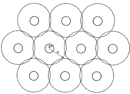
To help mitigate squeeze film damping, large plates are often perforated. This allows air to flow from the front side to the back and prevents large pressure from building up in between the surfaces. To model the pressure distribution for a perforated plate, the surface is broken into annular cells as shown in Figure 2-3.
%N %
- t N
Figure 2-3 - Approximation of a perforated plate with annular cells
Since the edge of the annulus is not actually an edge in the plate, special boundary conditions must be used. The pressure at a hole is low, because there is no resistance to flow, while the pressure is greatest at the edge of a cell. .Symnmetry between cells allows us to set the slope of the pressure to 0 at this point. Thus
P(b) = 0 and (2.20)
dP
- (a) = 0 . (2.21)
dr
The pressure distribution can be solved in each annulus by considering the results from before. Integrating over the pressure field gives a squeeze film force, from which the drag coefficient can be calculated as follows
csqrit-m = 32 (4fl2 _ fl4 - 4 ln(fl) - 3)N (2.22)
2x g
where Ac is the area of each annular cell, and #l = b/a, and fl is the gap height and N is the number of holes. It is worthwhile to compare the relative magnitudes of the damping coefficients. Taking the ratio, with the area for A substituted in the perforated plate equation and (gl = (4#l2 _ fl4 - 4lIn(#l) - 3) we get
= a N -- =--fN a(2.23)
where
N = 1 w W. (2.24)
The ratio simplifies to
Csqfilm 3 iwaz
Cbeam
16
S3L
The spacing between holes (and thus a) is determined by deciding the amount of the plate that should be holes
. Aholes wbz b2
(2.26)
Apiate -ira 2 a2
With the inner radius (b) set to the minimum (safely) resolvable size (about 2pm radii holes),
a = gratiohoiesb . (2.27)
An estimate of this ratio can be made by choosing reasonable dimensions based on fabrication and design limitations. The gap is limited to 2.5 pm because stress in the sacrificial oxide causes it to peel for thicker films. The ratio of holes to actuation area must be kept small to ensure that the proper actuation force is applied. For this estimate, the ratio will be assumed to be 10. Larger numbers of small holes decrease the squeeze film damping further. However it is difficult to DRIE etch narrow holes. Let b = 2 pm (=> a = 6.3 pm), which is small, but safely etched. For this ratio of b/a, (g -2. Finally, to ensure beam-like behavior, 1 = w = L/5. With these substitutions,
Csqfilm 24L
(2.28)
Cbeam 625
where the 24/625 factor has units of pm'. All devices considered have L E [500 pm, 1500 pm], which places the damping ratio roughly E [20, 551. This suggests that damping is dominated by the squeeze film effects at the end of the beam. This means that if the squeeze film damping is low enough that it won't impede the motion of the beam, then overall damping won't either. This does not mean that damping will have a negligible effect on the quality factor, but rather that it doesn't have an undue effect on the beam's motion.
The gap can only be made smaller and the holes can only get larger (see the fabrication limits above), both of which increase the squeeze film damping. Similarly, increasing I increases
the area (and thus N), while decreasing I decreases the output signal, and as such squeeze film damping will only become more prominent.
3 Design and Optimization
With a general design in mind (a resonant cantilever beam in a hermetically sealed cavity) and detection principle (quality factor is uniquely determined by the surrounding pressure), it remains to be determined: 1) how to actuate the cantilever beam and 2) how to sense its motion.
3.1 Assessment of Actuation Methods
There are many possible methods for actuating a cantilever beam, each coming with its own set of benefits and limitations as will be discussed below. Beyond assessing whether the actuation method would work for this design, if this pressure sensor is to be combined with other MEMS devices, actuation should occur within the device. Large external equipment should not be required, such as lasers or large external actuators. However, most MEMS devices are electrically powered and often have signal processing, so these external features are allowed.
3.1.1
Thermal, Magnetic and Piezoelectric Actuation
Thermal actuation typically involves a beam of two materials with different coefficients of thermal expansion. Since they are attached, neither material can expand at its desired rate, leading to a stress distribution that causes the beam to bend. This is commonly used in thermostats, but the slow heating/cooling time prohibits large scale use on the macro scale. However, microscale devices have much larger surface area to volume ratios, and can heat and cool much more quickly, with a maximum frequency on the order of 3kHz [27]. Actuation is often achieved through resistive heating, allowing actuators to be easily fabricated along with existing electronics. However, even the increased frequency of microscale cooling does not create a resonator that is fast enough for the design parameters.
A variant on thermal actuation involves heating the beam with a laser, rather than resistively. This has the added benefit that it can be integrated into any optical sensing techniques without any added equipment. However, it places some restrictions on the fabrication process because there must be an optical path to the cantilever, in addition to the switching time limitations mentioned above.
Magnets can in principle be used to actuate small structures. They can achieve large forces. However commercial magnets are too large and difficult to integrate into MEMS, and fabricating magnets in the clean room is very difficult. Fabricating an electromagnet on a wafer
has been done [28] but is quite challenging, while an external field defeats the purpose of a self-contained device. Additionally, the switching time for MEMS electromagnetic actuators is too low, with an estimated values similar to thermal bimorphs (<3kHz) [27].
Piezoelectric actuation is also commonly used in MEMS. By applying a voltage across a piezoelectric material, extremely large forces can be exerted to drive small displacements at high rates, up to the MHz range for a piezoelectric bimorph beam [27]. However, this runs into many of the same limitations of magnets. Commercial piezos are too large for this design and hard to interface with a microscale structure. While cleanroom processes exist for depositing lead zirconate titanate (PZT) and other piezoelectric films, the processes have low yield and are not compatible with many other cleanroom processes. Additionally, high temperatures must be avoided. Some commercial piezos can withstand temperatures as high as 8200C, though most are limited to <400*C [29]. Neither temperature is high enough for a quality fusion bond.
3.1.2 Electrostatic Actuation
Electrostatic actuation is a common method of actuation in MEMS [30]. The operating principle is simple - charge up two plates near each other and electrical attraction will exert a force on both objects. This has been used in devices as varied as Texas Instrument's Digital
Micromirror Device (DMD) [1] to MEMS microphones [311, and is regularly used to actuate resonators. The force can be greatly increased by combining multiple interleaved charged fingers to create a comb drive [27].
Electrostatics can exert large forces over short distances with very fast switching time, which make it a great option for a fast, high frequency (thus stiff) resonator. Additionally, fabrication is relatively simple compared to the other actuation methods - a single doping step can give both plates the necessary conductance.
However, an unexpected source of impedance in the actuation circuit, such as higher contact resistance, can cause an unanticipated decrease in voltage across the actuation gap if connected in series. Additionally, if sensing electrically as well, parasitic signals can interfere with the measured signal. Parasitic paths in series with the actuation circuit, caused by poor isolation between the terminals, allow the actuation voltage to interfere with the measured output signal.
Additionally, the electrostatic force F is nonlinear, which leads to some interesting effects. For parallel plates, the force F and electrical potential energy Ue, respectively, are
Fe = 22 and (3.1)
2g 2
Ue = (3.2)
where Eois the permittivity of free space, A is the area of actuation, V is the actuation voltage, and g is the current gap between plates. While the system is in equilibrium, the spring force
F, = k(go - g) balances Fe as follows
Fg 0 EAV2 k(g0 -g). (3.3)
Taking the derivative with respect to g yields the spring constant for the system (how much additional actuation force is needed to cause a small change in the gap)
3E0A V2
ksystem - 23 + k . (3.4)
As expected, with no actuation voltage the spring constant reduces to the stiffness of the beam. However, increasing the voltage actually decreases the apparent stiffness of the system, a phenomenon known as spring softening.
If we solve for the voltage from the sum of the forces above and substitute, we can see that ksystem becomes negative when actuated beyond g0/3. This point is unstable, any additional voltage will cause the beam to snap in. This instability is known as pull-in. This greatly limits the operating range for an electrostatic device. Since the stiffness decreases faster the closer the deflection is to the critical value, it is wise to only operate at small
deflections. Both spring softening and pull-in can be seen below in Figure 3-1 for a silicon beam with dimensions of 1100im x 220ptm x 15pm.
X10-6
Gap vs Voltage
2-1.5H 0.5H O0 Voltage [V]Voltage vs Frequency
5 Voltage [V] 10Figure 3-1 - (top) The nonlinear nature of electrostatic actuation can be seen in the first plot. Pull-in occurs at 14.65V, and can be seen in the first plot as the point where the gap goes to 0. (bottom) Spring softening caused by the decrease in the overall spring coefficient. Results are shown for an 1100im x 220ptm x 15pm silicon beam with a 2.5pm gap.
While electrostatic actuation can have lower actuation voltages or parasitic interference if the full circuit is not modeled correctly, and exhibits considerable nonlinear behavior, both of these problems can be avoided with careful design. Careful isolation and integrating the sensing into the actuation (see Third Harmonic Sensing below) can negate many of the harmful parasitic effects. By operating with small deflections, the full nonlinear behavior can be
approximated as linear (with a Taylor expansion) around the neutral point with an electrostatically softened spring constant.
A summary of these actuation methods is shown below in Table 3-1.
Table 3-1: Comparison of Actuation Methods
After considering all the actuation options, electrostatic actuation was chosen for the pressure sensor. All of the other options are either limited in operation or increase the
difficulty of device fabrication. Additionally, several of them require external actuators or equipment to operate, which is not compatible with a modular pressure sensor. While
electrostatic actuation isn't perfect either, the limitations can be worked around with a careful design and by limiting deflection to a small range, and actuation can be achieved solely with an externally applied voltage.
3.1.3 Beam Bending
3.1.3.1 Forced oscillations with damping
Before analyzing the full Euler-Bernoulli equation for dynamic beam bending, it is instructive to examine resonance for the case of forced oscillations of a linear spring (spring constant k) with damping (damping coefficient c). A general differential equation describing the motion is
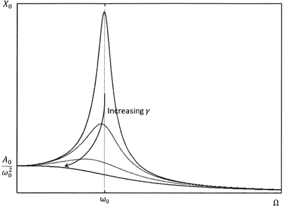
2 + 2yi + W2x = Aosin(flt) (3.5)
where y = c/2m is the damping factor, wo = k/rm is the resonance frequency, AO = FO/m is the magnitude of the acceleration for a force of FO and D is the forcing frequency. The solution
to this equation is given by:
x(t) = xs(t) + Xosin(flt + 0) (3.6)
where xs(t) is the specific solution (transient), and X0 is the magnitude of the forced vibration.
We want to consider the motions for t
>>
1/y after which the transient vibrations have died out. Substituting x(t) back into the differential equation, at large enough time we can say that the magnitude and phase can be written asA0
XO = and (3.7)
(wz _ f2)2 + 4y2W2
2yf2
tan(O) = 2 2 . (3.8)
A0
Figure 3-2 - Magnitude of resonance for several different levels of damping.
Typical measurement of the resonance peak assumes that peak width is the frequency range between which X > Xmax. This width, for small y, is
Af =0W (3.9)
0
7r
Increasingy
111
(00
Figure 3-3 - Phase response for several levels of damping
The maximum displacement for a given damping factor can be found by setting the derivative of XO to 0.
Xmax AA 0 2A0Q2
y z y 2 2
The forcing frequency that corresponds to the maximum value is 1
fimax = WO 1 -Q.
For high quality factors, this reduces to
(3.10) (3.11) AOQ Xmax -2 00 fmax =0 (FO/m) F0 - ) = and
While the mechanics of a damped moving beam actuated by a distributed load are certainly more intricate than those of a simple forced spring-mass-damper system, it will be assumed (3.12) (3.13)