Design and Analysis of Reconfigurable Analo
MASSACHUSETTS INSTITUTE OF TECHw ,OLo-y
System
by
MARIO
2C11
Payam Lajevardi
L BRARIES
B.A.Sc. Electrical Engineering, University of British Columbia,'2003
and
S.M. Electrical Engineering, Massachusetts Institute of Technology,
2005
Submitted to the Department of Electrical Engineering and Computer
Science
in partial fulfillment of the requirements for the degrees of
Doctor of Philosophy
at the
MASSACHUSETTS INSTITUTE OF TECHNOLOGY
February 2011
@
Massachusetts Institute of Technology 2011. All rights reserved.
A uthor ... -.. ----....----..
Department of Electri<al Engineering and Computer Science
-
- OctAvber 18, 2010
Certified by...---... - -.
Anantha P. Chandrakasan
Joseph F. and Nancy P. Keithley Professor of Electrical Engineering
Thesis jupervisor
Certified by ...
...
Hae-Seung Lee
Professor of Electrical Engineering
Thesis
Supervisor
Accepted
by...-Terry P. Orlando
Chairman, Departmental Committee on Graduate Students
Design and Analysis of Reconfigurable Analog System
by
Payam Lajevardi
Submitted to the Department of Electrical Engineering and Computer Science on August 29, 2010, in partial fulfillment of the
requirements for the degrees of Doctor of Philosophy
Abstract
A highly-configurable analog system is presented. A prototype chip is fabricated
and an ADC and filter functionalities are demonstrated. The chip consists of eight identical programmable stages.
In an ADC configuration, the first five stages are programmed to implement a 10-bit ADC. The ADC has ENOB of 8 10-bits at 50 MSPS. The ENOB improves to 8.5 10-bits if the sampling rate is lowered to 30MSPS. The ADC has an FOM of
150fJ/conversion-step, which is very competitive with the state of the art ADCs. The first stage is responsible for 75% of the input-referred noise power. The sampling noise is respon-sible for 40% of the total noise power and the zero-crossing detector is responrespon-sible for
60%.
The chip is tested in two different filter configurations. In one test, the first two stages of the chip are configured as a second order Butterworth filter and the third stage is configured as an amplifier. In another test, the first three stages of the chip are programmed as a third-order Butterworth filter. The desired filter functionalities are demonstrated in both configurations. It is shown that in a third order Butterworth filter, more than 90% of the noise is due to the zero-crossing detector of the last stage. This is mainly due to the fact that the noise of earlier stages is filtered with the filter transfer function, but the noise of the last stage is not filtered.
The ZCBC architecture has been used to avoid the stability problems and scale power consumption with sampling frequency. A new technique is introduced to im-plement the terminating resistors in a ladder filter. This technique does not have any area or power overhead. An asymmetric differential signaling is also introduced. This method improves the dynamic range of the output signals, which is particularly important in new technology nodes with low supply voltage.
Thesis Supervisor: Anantha P. Chandrakasan
Title: Joseph F. and Nancy P. Keithley Professor of Electrical Engineering Thesis Supervisor: Hae-Seung Lee
Acknowledgments
I would like to thank Professor Anantha Chandrakasan and Professor Harry Lee for
their support. I enjoyed the learning opportunity in their research group and under their supervision and guidance. I would also like to thank other members of Anantha group and Harry Lee group whose valuable input have enhanced my insight in my research. In addition, I would like to thank IBM and TSMC, which provided us with fabrication facilities.
I would like to thank my parents, Soraya Mohammadi and Hosein Lajevardi, and
my brother, Pedram Lajevardi, for their support and love. Most important, I would like to thank my wife, Laila Jaber Ansari for her ultimate love and support.
The funding was provided by DARPA and the Center of Integrated Circuits and Systems (CICS) at MIT. We acknowledge chip fabrication through DARPA and the
Contents
1 Introduction 1.1 ADC Review ... 1.1.1 Pipeline ADC . . . . . 1.1.2 Over-Range Protection 1.2 Filter Review . . . .1.2.1 Passive Ladder Filter
1.2.2 Active Ladder Filter
1.2.3 Thesis Contribution.
2 Zero-Crossing-Based Circuits
2.1 Advantages of ZCBCs . . .
2.2 Sources of Nonlinearity . . .
2.3 Solution to some Challenges
. . . . . . . . in Pipeline ADC . . . . . . . . . . . . . . . . (ZCBC)
3 System Architecture and Implementation
3.1 System Description . . . .
3.1.1 The Need for ZCBC Implementation . . .
3.1.2 Implementation of a Reconfigurable Stage
3.1.3 ADC Configuration . . . . 3.1.4 Filter Configuration . . . . 3.2 System Components . . . . 3.2.1 Sampling Circuit . . . . 3.2.2 Bootstrapping . . . . 19 20 21 22 23 24 25 27 37 37 39 41 42 43 43 44 47 . . . . . . . . . . . . .
.-3.2.3 Zero-Crossing Detector . . . . . . . . . . . 48
3.2.4 Current Sources . . . . 49
3.2.5 The first Stage . . . . 51
3.2.6 Bit-Decision-Comparators (BDC) . . . . 51
3.2.7 Residue Plot . . . . 52
3.2.8 The Analog Buffer . . . . 53
3.2.9 Terminating Resistors . . . .. 54
3.3 Asymmetric Differential Signaling . . . . 57
3.4 Programmability . . . . 58
3.4.1 Programmability for functionality . . . . 58
3.4.2 Programmability for Calibration . . . . 59
3.4.3 Programmability for Power Optimization . . . . 60
3.5 System Simulation . . . . 60
4 Noise Analysis 65 4.1 Noise Review . . . . 65
4.1.1 Sampling Noise (kT/C Noise) . . . . 66
4.1.2 Effective Number of Bits (ENOB) and Figure of Merit (FOM) 68 4.1.3 Noise Gain . . . . 69
4.1.4 Noise Bandwidth (NBW ) . . . . 70
4.1.5 Noise of an amplifier . . . . 70
4.1.6 Noise Aliasing . . . . 71
4.2 Noise of the ADC . . . . 73
4.3 Filter Noise . . . . 76
4.3.1 Noise of an Integrator . . . . 76
4.3.2 Noise Transfer Function . . . . 78
4.4 Coupling Noise . . . . 82
4.4.1 Noise on Reference Voltages . . . . 83
4.5 Conclusion . . . . 85
5 Sensitivity of the System 87
5.1 Sensitivy to Capacitance Values . . . . 87
5.1.1 ADC Configuration . . . . 87
5.1.2 Filter Configuration . . . . 88
5.2 Offset of the Zero-Crossing Detector . . . . 90
5.3 Offset in an ADC Configuration . . . . 90
5.4 Offset in a filter Configuration . . . . 91
5.5 C onclusion . . . . 95
6 Measurements of the Fabricated Chip 97 6.1 ADC Measurement . . . . 98 6.2 Filter Measurement . . . . 106 6.3 Cost of Reconfigurability . . . . 108 6.3.1 Power Consumption . . . . 109 6.3.2 Speed . . . .. 111 6.3.3 A rea . . . . 112 6.3.4 N oise . . . . 113 6.3.5 Choice of Architecture . . . . 114 6.4 Measurement Summary. . . . . 115 7 Conclusions 119 7.1 Future W ork . . . . 121
7.1.1 Pulse-Width Modulated Signals . . . . 122
7.1.2 Programmable Feedback Ratio Using Programmable Current Sources . . . . 122
A The Script to Program the Chip 127
B Noise Bandwidth Calculation 141
D Noise of an Amplifier with Parasitic Capacitance on Virtual Ground
List of Figures
1-1 ADC Architecture for different sampling rates and resolution [14]. . 21
1-2 Block diagram of one stage of a pipeline ADC . . . . 22
1-3 The relationship between the input and output signals for each stage of a pipeline ADC when the sub-ADC has 2-bit resolution (n=2). . . 23
1-4 The effects of the offset of the sub-ADC threshold levels on the output voltage. . . . . 24
1-5 Over-range protection to provide margin for sub-ADC threshold levels. 25 1-6 Passive implementation of a fifth-order low-pass ladder filter. . . . . . 25
1-7 Passive implementation of a high-pass ladder filter. . . . . 26
1-8 Passive implementation of a band-pass ladder filter. . . . . 26
1-9 Passive implementation of a band-pass ladder filter. . . . . 27
2-1 Basic opamp-based amplifier. . . . . 32
2-2 Basic zero-crossing based amplifier. . . . . 33
2-3 Spliting the output current source. . . . . 36
3-1 Block Diagram of an Ideal System. . . . . 38
3-2 Amplification and integration using the same switched-capacitor circuit. 40 3-3 Building block of a pipeline ADC. . . . . 40
3-4 Building block of an active ladder filter . . . . 41
3-5 Schematic of an active ladder filter. . . . . 41
3-6 Basic building block of reconfigurable stage. . . . . 42
3-7 Single-ended bottom-plate sampling circuit. . . . . 44
3-9 3-10 3-11 3-12 3-13 3-14 3-15 3-16 3-17 3-18 3-19 3-20 3-21 3-22 3-23 3-24 3-25 4-1 4-2 4-3 4-4 4-5 4-6 4-7 4-8 4-9 4-10 4-11 4-12
A basic sampling circuit. . . . .
Circuit model of the noise of a sampling circuit. . . . . . General block diagram of a system with transfer function Thermal Noise of a MOSFET. . . . . Basic differential amplifier and its sources of noise. . . . . The block diagram of signal sampling. . . . .
Time domain representation of the sampling signal. . . .
Frequency domain representation of the sampling signal. Frequency domain presentation of the sampling signal. Schematic of a switched-capacitor integrator. . . . . Noise model of the integrator. . . . . Block diagram of a third order low-pass filter. . . . .
. . . . 66 . . . . 67 of H(s). . . 69 . . . . 71 . . . . 72 . . . . 72 . . . . 73 . . . . 73 . . . . 74 . . . . 77 . . . . 78 . . . . 79
Resistance variation of different switches. . . . . Schematic of bootstrap circuit. . . . . Simulation of the bootstrap circuit. . . . . Schematic of zero-crossing detector. . . . . Schematic of a basic current source. . . . . Basic building block of reconfigurable stage. . . . . Schematic of a bit-decision-comparator. . . . . Residue plot in ADC configuration. . . . . Residue plot of the first stage in ADC configuration... The schematic of the analog buffer. . . . . Implementation of terminating resistors in ladder filters. . . Signal swing in zero-crossing based circuits. . . . . Timing of different phases of clock and pulses. . . . . The power supply model. . . . . Simulated ADC performance when a near Nyquist-rate input Estimated INL of ADC from simulation. . . . . Third order Butterworth filter frequency response. . . . . . . . . . 46 . . . . . 47 . . . . . 48 . . . . . 49 . . . . . 50 . . . . . 52 . . . . . 53 . . . . . 54 . . . . . 55 . . . . . 56 . . . . . 57 . . . . . 58 . . . . . 59 . . . . . 61 is applied. 62 . . . . . 63 . . . . . 63
4-13 Block diagram of a third order low-pass filter with sources of noise. . 4-14 Noise transfer function of integrators input noise in a third order
But-terworth filter . . . . ... . . . .
4-15 Noise transfer function of integrator output noise in a third order But-terw orth filter .. . . . . 4-16 Noise of reference voltage based on simulation. . . . . 4-17 The currents that passes through Vcm in a fully differential circuit. .
5-1 Residue plot of a stage with no gain error. . . . .
5-2 Residue plot of a stage with gain error. . . . . 5-3 ADC transfer function when the gain of each stage is larger than the
ideal gain . . . . .
5-4 ADC transfer function when the gain of each stage is smaller than the
ideal gain . . . . .
5-5 Transfer function of a third order butterworth filter with 20% mismatch
on only one integrating capacitor. . . . .
5-6 Transfer function of a third order butterworth filter with 20% mismatch
5-7 5-8 5-9 6-1 6-2 6-3 6-4 6-5 6-6 6-7 6-8 on terminating resistors. . . . . Passive implementation of a low-pass ladder filter. . . . . Active implementation of a low-pass ladder filter. . . . . Block diagram of an active low-pass filter with the corresponding input referred offset of each integrator .. . . . .
The die photo of the core that consists of eight stages. . . .
The block diagram of the fabricated chip. . . . .
Layout of one stage. . . . .
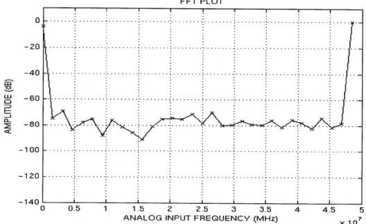
The chip configuration for test as an ADC. . . . . FFT plot of the ADC output with a 1MHz sinusoidal input. FFT plot of the ADC output at a near Nyquist rate... The INL of the ADC with 10-bit quantization levels. . . . . The FFT plot of the ADC output with grounded inputs. . .
. . . . 98 . . . . 98 . . . . 99 . . . . 100 . . . . 101 . . . . 102 . . . . 103 . . . . 104
6-9 The ADC ENOB at different sampling rates... 105
6-10 The power consumption and the FOM of the ADC as a function of the sam pling frequency. . . . 106
6-11 The ADC ENOB at different ramp rates. . . . 107
6-12 The ENOB as a function of the input signal frequency. . . . 108
6-13 The SFDR as a function of the input signal frequency. . . . 109
6-14 The ENOB as a function of the input signal amplitude. . . . 110
6-15 Comparison of state of the art non-reconfigurable ADCs (ISSCC 2007-2010) with this work. . . . 111
6-16 The chip configuration for test as a second order filter. . . . 112
6-17 Ideal and measured filter transfer function for a second order butter-w orth filter. . . . 113
6-18 The chip configuration for test as a third order filter. . . . 114
6-19 Ideal and measured filter transfer function for a third order butterworth filter. . . . 115
6-20 The main tone and its harmonic at the output of the ADC that mea-sures the output of a third order low-pass filter. . . . 116
7-1 Two stages of ZCBCs with the corresponding signals. . . . 123
7-2 Time-domain representation of Vsi and Vcont,o that send an analog signal from one stage to the next stage. . . . 124
7-3 Programmable capacitor in the feedback of a ZCBC circuit. . . . 125
7-4 Alternate method to implement a programmable capacitor in the feed-back of a ZCBC circuit. . . . 125
7-5 Simplified method to implement a programmable capacitor in the feed-back of a ZCBC circuit. . . . . 126
A-1 The script to program the chip Part 1. . . . 128
A-2 The script to program the chip Part 2. . . . 129
A-3 The script to program the chip Part 3. . . . 130
A-5 The script to program the chip A-6 The script to program the chip A-7 The script to program the chip A-8 The script to program the chip A-9 The script to program the chip A-10 The script to program the chip A-11 The script to program the chip A-12 The script to program the chip A-13 The script to program the chip
Part 5. Part 6. Part 7. Part 8. Part 9. Part 10. Part 11. Part 12. Part 13. . . . . 132 . . . . 133 . . . . 134 . . . . 135 . . . . 136 . . . . 137 . . . . 138 . . . 139 . . . . 140
B-1 Integral calculation by mathematica . . . .
C-1 Block diagram of a third order low-pass filter with sources of noise.
D-1 Schematic of an amplifier. . . . . D-2 Phase 2 of the amplifier. . . . .
142 144 146 146
List of Tables
1.1 Equivalent state variables in the passive filter and the active filter. . 27
1.2 Equivalent equations in the passive filter and the active filter. . . . . 28
1.3 The value of the components in the active filter based on the value of
their corresponding components in the equivalent passive filter. . . . . 29
3.1 Ratio of feedback capacitor to the sampling capacitor for each stage of
filter and different types of filters. . . . . 43
3.2 Offset adjustment of ZCBC detector based on the programmable load
of the first stage. ... ... 50
3.3 Offset adjustment of bit-decision-comparator. . . . . 53
4.1 Noise bandwidth of low-pass filters when all poles are located at the
sam e frequency. . . . . 70
6.1 Cost of Reconfigurability.. . . . . . . . . 117
6.2 Summary of Measurements. . . . 117
B.1 Noise bandwidth of low-pass filters when all poles are located at the
Chapter 1
Introduction
While digital FPGAs provide a fast and cost-efficient method to prototype digital circuits, the development of similar system for analog circuits is still limited because it is difficult to realize a programmable analog system that can be configured to wide variety of analog circuits. A highly programmable analog system that can be config-ured for an arbitrary analog functionality is very valuable. Many electronic devices use multiple communication standards. As the number of communication standards are growing rapidly, electronic devices tend to incorporate more communication stan-dards, which increases the cost of the system. To integrate multiple standards on the same chip, a highly-programmable analog system can replace the analog blocks of all these systems. In addition, highly-programmable analog systems can be used as the analog core of software defined radios (SDR) to perform its required analog function-alities such as analog to digital conversion (ADC), filtering, and programmable gain amplification. Clearly, SDR requires programmable radio frequency circuits as well (such as programmable mixer, low-noise amplifier, oscillator). Highly programmable analog systems can also be used in fast prototyping of analog systems. They can also be used for educational purposes (similar to digital FPGAs that are used in educational implementation of digital systems).
Field programmable analog arrays (FPAA) have been previously proposed [1] . It
uses continuous-time blocks whose gain is programmable by changing transconduc-tance of amplifiers. Programmable connectivity between analog circuits is a major
challenge in reconfigurable analog systems. It uses permanent connection between adjacent blocks and sets the gain of adjacent blocks to zero to effectively discon-nect them. Another implementation uses programmable transconductance and pro-grammable capacitor to control the gain of stages [2]. A propro-grammable ADC that can be configured as sigma-delta or pipeline employs programmable capacitors, pro-grammable connectivity, and adjustable biasing [3]. This project demonstrates a highly-reconfigurable analog system that can be used to implement pipeline ADCs and switched-capacitor filters. Zero-crossing based circuits (ZCBC) are utilized for superior power efficiency and reconfigurability.
In the rest of this chapter, ADCs and switched-capacitor filters are reviewed. In Chapter 2, zero-crossing based circuits are described. Chapter 3 describes how the system is implemented. Chapter 4 analyzes the noise of the system and Chapter 5 reviews the sensitivity of the reconfigurable system to capacitor mismatch and to the offset of the zero-crossing detectors. Chapter 6 describes the measurement results of
the fabricated chip and Chapter 7 concludes the thesis.
1.1
ADC Review
An analog to digital convertor (ADC) converts an analog signal to its correspond-ing digital code. Main ADC architectures include flash ADCs [4][5][6], successive-approximation-register ADCs [7][8], pipeline ADCs [9][10], sigma-delta ADCs [11], and time-interleaved ADCs [12][13]. As shown in Figure 1-1, each architecture is more suitable for a particular range of sampling rate and resolution [14]. Flash and time-interleaved ADCs are suitable for higher speeds than pipeline ADCs (which is not shown on Figure 1-1). There is an overlapping area where more than one archi-tecture may be suitable. Pipeline ADCs are chosen for this research to cover medium to high speed and resolution range.
INDUSTRIAL ,-MEASUREMENT 2 4 --22- -o"AU 20- -,AOUSTO . . .. . ... HIGH SPEED: Z18 INSTRUMENTATION, O VIDEO, IF SAMPLING,
F ~16 6 - SOFTWARE RADIO, ETC.
(0
W
14-
12-MEASUREMENT
STATE OF THE ART
10- (APPROXIMATE)
10 100 1 k 10k 100k IM I OM IlOOM 1G
SAMPLING RATE (Hz)
Figure 1-1: ADC Architecture for different sampling rates and resolution [14].
1.1.1
Pipeline ADC
Pipeline ADCs consist of several identical stages that are cascaded. The block dia-gram of each stage is shown in Figure 1-2. Each stage is composed of four components, a ADC, a digital-to-analog convertor (DAC), an adder, and an amplifier. A
sub-ADC is usually an sub-ADC with limited number of quantization levels, n. For example,
it may be a flash ADC with only one or two bits, while the overall pipeline ADC may have 10-14 bits.
When an analog signal is converted to a digital code, there is a difference be-tween the amplitude of the analog signal and the amplitude of the digital code. The difference is due to the limited number of the bits in the digital code and is called quantization error. As the number of the digital bits increases, the quantization error reduces.
In pipeline ADCs, the sub-ADC has a limited resolution. To increase the overall resolution of a pipeline ADC, the quantization error of the sub-ADC is sent to the
Vin
sub-ADC -- DAC x AVout
n
Digital CodeFigure 1-2: Block diagram of one stage of a pipeline ADC
subsequent stages. Subsequent stages convert the quantization error of earlier stages to the corresponding digital codes and add it to the overall digital output. As a result, each cascaded stage increases the resolution of the ADC. To find the quantization error of each stage, V, the output of the sub-ADC is sent to a DAC and subtracted
from the input signal as shown in Figure 1-2. Since the amplitude of V is small, it is
typically amplified. If n is the number of the bits of the sub-ADC, the range of V is
smaller than the full-scale input range by a factor of -L. If it is desired that Vin and Vst have the same range, the amplifier should have a gain of 2n. This is usually the case for pipeline ADCs utilizing identical stages. Figure 1-3 shows the relationship between the input and output of each stage and the corresponding digital code if the
sub-ADC has 2-bit resolution.
To construct the digital output code of a pipeline ADC, the output of each stage should be multiplied by the gain of earlier stages and added to the final digital code.
If a pipeline ADC has k stages, and each stage has n quantization bits (Di for stage
i), the digital output code of the ADC is given by:
ADCcode D1 + D2 * 2n + D3 * 22n + ... + Dk * 2(k-1) (1. 1)
1.1.2
Over-Range Protection in Pipeline ADC
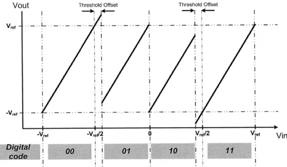
The sub-ADC may have an offset in its threshold voltages for different digital codes
Vout
-Vre -V A2 Vr 2 V,
00 1 01 1 10 11
Figure 1-3: The relationship between the input and output signals for each stage of a pipeline ADC when the sub-ADC has 2-bit resolution (n=2).
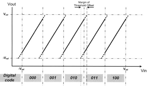
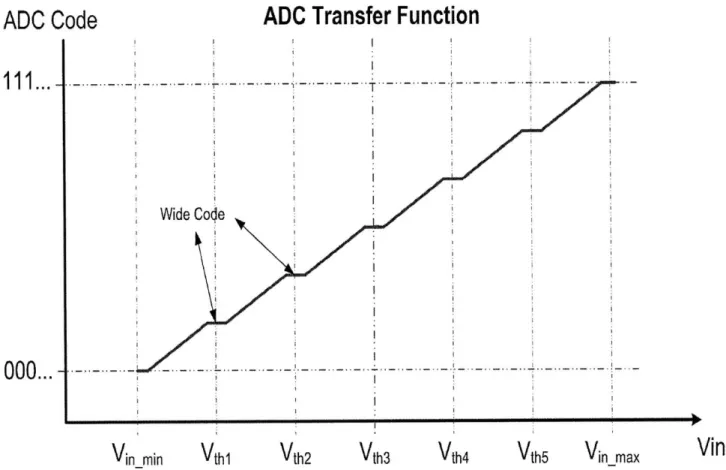
or -Vef) of subsequent stages for some values of Vm,. In that case, the subsequent stages cannot resolve the input voltage in the region that saturates the subsequent stage. To avoid this problem, the threshold voltages of the sub-ADC are chosen so that the output does not exceed Vef or -Vef as shown in Figure 1-5. If needed, the number of threshold levels can be increased. This method provides some margin of error for the threshold of the sub-ADC digital codes.
1.2
Filter Review
There are two main architectures to implement switched-capacitor filters, biquad filters [15] and ladder architecture [16]. Since this chip is intended to implement any arbitrary filter, the exact functionality of each stage is not known a priori. For example, the order of the filter and its cutoff frequency are programmable. Since biquad-based filters are sensitive to capacitor matching [16], ladder filter architecture is used in this research.
Vout Threshold Offset Threshold Offset
IVe -V :f2I
-v 2'2fv/ Vin
Dgtl00 01 1 10 1
code
Figure 1-4: The effects of the offset of the sub-ADC threshold levels on the output voltage.
1.2.1
Passive Ladder Filter
Figure 1-6 shows a passive ladder filter. The number of storage components (capaci-tors, and inductors) determines the order of the filter and the type of the components determines the type of the filter. For example, Figure 1-6 shows a low-pass filter. If the capacitors are replaced with inductors, and the inductors are replaced with
ca-pacitors, a high-pass filter is obtained
(Figure
1-7). Similarly, replacing capacitors inFigure 1-6 with a parallel combination of a capacitor and an inductor, and replacing the inductor with a series combination of a capacitor and an inductor results in a band-pass filter (Figure 1-8). The value of the capacitors, inductors, and the resistors determine the cut-off frequency of the filter and the shape of the filter (e.g. Butter-worth, Chebyshev, and Elliptic). The design of ladder filters is researched extensively
[17][18].
The value of each component in the ladder filters can be easily determined with software as well [19].* .1 I I I I I I I I 1/ I I Margin of Thehold Offset V:I (. ~Vmf V00 000 010 011 Vin
Figure 1-5: Over-range protection to provide margin for sub-ADC threshold levels.
Vin
Vout
Figure 1-6: Passive implementation of a fifth-order low-pass ladder filter.
1.2.2
Active Ladder Filter
An opamp-based implementation of the low-pass ladder filter is shown in Figure 1-9 as proposed by [16]. This architecture is used to implement filters in this chip. In this section, first it is shown that the passive filter in Figure 1-6 and the active filter in Figure 1-9 are equivalent. Then, it is described how to determine the value of different components in the active filter, if the value of all components in the equivalent passive filter is known.
In Figure 1-6, the state variables are, V11, i12 , V13, i14, and Vt. Each state
variable can be written in terms of other state variables and the input. For example, Vout
Vref
--Vret
-'I I.
R1 C
Vin
L1
L2 R2 Vout
Figure 1-7: Passive implementation of a high-pass ladder filter.
C2
L
2C4
L
4R
1C
Vin L i~ C1C3
VoutL5
C
51-8: Passive implementation of a band-pass ladder filter.
V11 can be written as a function of other state variables as in Equation 1.2. For
simplicity, it is assumed that R1 = 1 and R5 = 1.
dVnj _ AVn 1
dt At C1 ( n- Vn i1 2) (1.2)
In Figure 1-9, the state variables are,
%21,
V22 , V23, V24, and V1ot. In the activefilter, V21 is equivalent to V1 in the passive filter. V21 can be written as a function
of other state variables as in Equation 1.3. For simplicity, it is assumed that all the sampling capacitors have a unit value.
1
V%1 z= C(1K - V 1 -V22)
0A2 21 n 2 (1.3)
Table 1.1 shows the equivalent state variables in the two filters. In order to make Equation 1.2 and Equation 1.3 equivalent state equations in the two circuits, the
relationship between C21 and C11 should be:
Figure
R2 L3
C2 1 - - Cn fi
At
where At in the passive filter is equivalent to the period of each clock cycle in the active implementation. Table 1.2 shows the equivalent state equations for the two circuits. Since the state equations are equivalent, the two circuits are equivalent as well. Table 1.3 shows the value of each component in the active filter based on the value of its corresponding compoent in the passive filter.
V2 V24
Figure 1-9: Passive implementation of a band-pass ladder filter.
Table 1.1: Equivalent state variables in the passive filter and the active filter.
Passive filter Active filter
Vn1 V21 i12 V2 2 V13 V23 i14 V24 vout out
1.2.3
Thesis Contribution
In this research, a new architecture for a reconfigurable analog system is proposed. This architecture is suitable to implement an ADC and low-pass ladder filters. Zero-crossing based circuits are used for the first time to implement a reconfigurable sys-tem. It is also the first time that filter functionality is achieved with zero-crossed (1.4)
filter and the active filter.
based circuits. One unique characteristic of the proposed system is that the power consumption scales linearly with the sampling rate.
Asymmetric signaling is introduced for the first time to increase the dynamic range of ZCBCs. In addition, a new technique is introduced to implement the terminating resistors of a ladder filter. This technique improves the programmability of the system and reduces the complexity and area overhead of each stage.
The noise of the system is analyzed in both ADC and filter configurations. The dominant sources of noise are identified and their noise contributions are quantified.
In addition, the sensitivity of the system to capacitor mismatch and the offset of
zero-crossing detector is analyzed.
Finally, a chip is fabricated to show the ADC and filter functionality. Many measurements are performed to characterize the chip. The cost of reconfigurability is also estimated for the fabricated chip.
Table 1.3: The value of the components in the active filter based on the value of their corresponding components in the equivalent passive filter.
Value of components in the active filter C21 Cnl.f clk
C22 = L12.f clk
C23 = C13.f clk
C24 = L14.f clk
Chapter 2
Zero-Crossing-Based Circuits
(ZCBC)
Figure 2-1 shows an opamp-based circuit that amplifies its input. The analog input
signal is sampled across C1 and C2 in phase 1. The opamp-based circuit transfers the
charge on capacitor C2 to capacitor C1 in phase 2. As a result, the output voltage is
equal to the amplified input signal. In a negative feedback configuration, the value of differential input voltage of an opamp is close to zero. If the positive input of the opamp is connected to the ground instead of V,,, the voltage at node V, is nearly the same as the ground without direct connection to the ground. Therefore, it is referred to as a virtual ground. The terminology is used even when the positive input of the opamp is not connected to the ground. In general, the condition in which the differential input of an opamp has zero value is referred to as virtual ground condition. The same functionality can be implemented using zero-crossing-based circuits (ZCBC) as shown in Figure 2-2 and proposed by [20],[21],[23],[24]. The opamp is replaced by a combination of a current source and a zero-crossing detector. Unlike an opamp that continuously forces virtual ground condition, ZCBCs detect the virtual
ground condition. To do this, the output starts from one extreme voltage (Vdd or
ground) and swings toward the other extreme voltage. The zero-crossing detector continuously monitors its differential inputs. When the virtual ground condition is
output voltage waveform does not affect the accuracy of the circuit. If the zero-crossing detector has a constant delay, the overshoot of the output voltage depends on the delay and the slope of the output voltage when virtual ground condition is detected. In this case, a linear output waveform yields the best performance because with a constant delay and a constant slope at the output, the overshoot is always constant. Many analog circuits including ADCs and filters tolerate a constant offset at the output voltage as long as the output does not saturate.
In Figure 2-2, an analog input is sampled across C1 and C2 in a sampling phase
(phase 1). In the charge-transfer phase (phase 2), the input is amplified. To do so, the output is preset first. Then, the current source turns on. Since the current source provides a constant current and the load is capacitive, the output voltage is a linear ramp. The zero-crossing detector opens the sampling switch of the next stage when virtual ground condition is detected.
One difference between ZCBCs and opamp-based circuit is the way the output can be sampled. While the output of opamp-based circuits is ready for sampling during phase 2 of the current clock cycle and phase 1 of the next clock cycle, the output of ZCBCs can be only sampled during phase 2 of the current clock cycle.
Phase 2 V 0 1 vo[n] --- - ---Ii C1 Vin 1 C2 y
--r
v_+
V0 VCM M> Vre VxO i tPhase 2 V0 Vo[n] ...--- .--- .-t C1 y Vin 1 C2 ... ... 1 +~ e 2 resett reset, Sdd 0 t
Figure 2-2: Basic zero-crossing based amplifier.
2.1
Advantages of ZCBCs
ZCBCs have several advantages. One important advantage is its lack of explicit feedback. Since opamp-based circuits have negative feedback and more than one pole, the stability of the circuit is an important issue, and often requires large power consumption. If the load or the feedback ratio of the circuit is variable, the frequency compensation should be designed for the worst case situation. In ZCBCs, since there is no explicit feedback, there is no stability concern even with widely varying load and feedback condition.
While the speed of transistors improves in the new technology nodes, the intrinsic gain of transistors degrades. Since large open-loop gain is desired for opamps, the design of opamps is more challenging in new technology nodes. One method to increase the gain is by cascading several gain stages which deteriorates the stability of the system because of more poles. Another method to increase the gain of an opamp is cascoding which is challenging with low supply voltage in new technology nodes. As a result, opamp-based circuits are harder to design in new technology nodes. ZCBC is more suitable for new technology nodes since the current source and
the zero-crossing detector can be optimized independently. Zero-crossing detector can use cascaded stages for higher gain since stability is not a concern.
Finally, the power consumption of ZCBCs scale with the sampling frequency. This is due to the fact that once virtual ground condition is detected, all parts of the analog circuit including the current sources and zero-crossing detector turn off and the circuits do not consume static power any longer. As a result, if the circuit operates at a much lower speed, the power consumption scales accordingly. The power consumption of opamp-based circuits can also scale by adjusting its bias currents. However, the power consumption of ZCBCs can be adjusted for a very wide range of sampling frequencies.
2.2
Sources of Nonlinearity
There are several sources of nonlinearity in ZCBCs [23]. The first source of nonlin-earity is the delay of the zero-crossing detector. The delay causes an overshoot at the output. If the output is a linear ramp, a constant delay of zero-crossing detector gen-erates a constant overshoot and can be treated as a constant offset. However, delay variation of zero-crossing detector from one clock cycle to another (for example, due to common-mode variation) causes overshoot variation, which causes an error at the output.
In new technology nodes, the output resistance of current sources are low. As a result, when the output voltage changes, the current of the current source does not stay constant and the slope of the output voltage does not stay constant either. The nonlinearity of current sources causes signal-dependant overshoot variation. This gives a similar effect to that of finite gain in opamps. In addition, voltage-dependent capacitive load introduces nonlinearity at the output ramp, which causes overshoot variation. In this chip, the size of the linear capacitive load is much larger than the nonlinear parasitic capacitors. The delay of the zero-crossing detector is also sensitive to the common mode voltage variation and the ramp rate at its input.
approaches to zero with time. As a result, the voltage drop on the sampling switches is negligible. In ZCBCs, the current that passes through the sampling switches stays constant during the sampling period. As a result, there is a voltage drop across the switches during the sampling time. If the output current source provides a constant
current and the switch has a constant resistance, the voltage drop is constant and causes an offset. However, current sources have a limited output resistance (especially in new technology nodes). In addition, the resistance of switches changes widely with the input voltage; as a result, there is a variation on the voltage drop of the sampling switches, which causes an error at the output and the corresponding nonlinearity.
2.3
Solution to some Challenges
There are several techniques to improve the linearity of ZCBCs. One technique is to use multiple ramps as opposed to one [23]. The first ramp is a coarse search for virtual ground, and the next ramp(s) is (are) fine search. Since the ramp rate decreases after the first ramp, there is less sensitivity to the delay variation of the zero-crossing detector. The overshoot is also smaller because of slower ramp rate, which corresponds to a smaller error at the output and a smaller offset.
Another technique to improve the linearity of ZCBCs is to split the output current source in three sections [24] as shown in Figure 2-3. The output current source of the first stage (10) should drive the capacitive load of the first stage (Cn in series
with C12) and the input capacitance of stage 2 (C21 in parallel with C22). A large
current that charges C21 and C22 passes through switch 1 and switch 2 and causes a
large voltage drop on those switches. Two current sources (I1 and 12) are added after
switch 1 and switch 2 to provide the current to capacitors C21 and C22 and 1o is reduce
to provide current only to the capacitors in stage 1. In case of mismatch between 1o,
I1, and '2, the mismatch current between the current sources passes through switch
1 and switch 2. The mismatch current is much smaller than the total current. Note
that I1 and I2 are controlled with the same signal that controls 1o. Since the current
Stage 2
Switch 2
Gi'Vc h
Switch 3
Figure 2-3: Spliting the output current source. well.
Stage I
Chapter 3
System Architecture and
Implementation
In this chapter, the architecture of the system is described and it is shown how different functionalities are implemented. Then, the implementation of individual circuit blocks is reviewed. A new technique is described to implement the termination resistor in the filter. In addition, asymmetric differential signaling is introduced which increases the dynamic range of the signal. Finally, full system simulation for a 10-bit
ADC and a third-order Butterworth filter are presented.
3.1
System Description
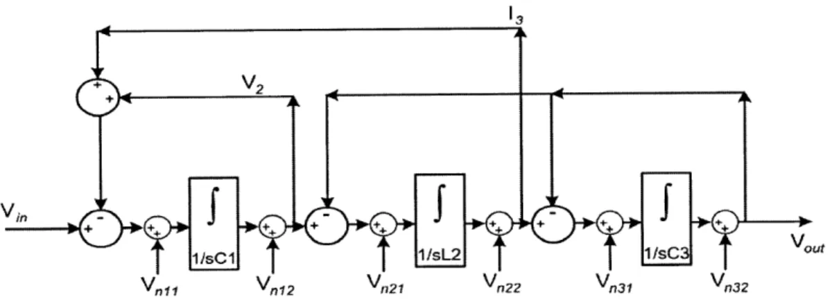
Figure 3-1 shows the block diagram of the ideal system. It consists of configurable analog blocks, programmable switches, and the configuration block. Configurable analog blocks have both amplification and integration functionality. Unlike digital FPGAs, the required connectivity of analog blocks is limited (both in terms of number of connections and the distance between source and destination blocks). As a result, the switches are placed only between adjacent blocks.
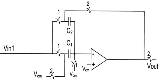
Figure 3-2 shows how an opamp-based switched-capacitor circuit can either
'411
EH"
iH
T T
LJLLJrJHJ JL
Figure 3-1: Block Diagram of an Ideal System.
during phase 1, the total charge across the capacitors in phase 1 is given by:
Q[n]
= (C1 + C2)1i[n] (3.1)The charge on C1 is transferred to C2 in phase 2. The output at the end of phase 2
is:
Vot[n + 1/2] = 2V. 1[n]
C2
(3.2)
Thus, the circuit performs amplification during phase 2.
If the input signal is only sampled on capacitor C1 without resetting the integration
capacitor (C2), the charge on capacitors C1 and C2 are given by:
Qc1[n]
= C1 V%1[n]Qc2[n] = Qc2[n - 1/2]
(3.3)
(3.4)
The charge on C1 is transferred to C2 in phase 2. The output at the end of phase 2
10
swfth
NoCk
10
is:
C1 Vi 1[n] + QC2[n - 1/2] -C
Vo0tn-+ 1/2- 0 2 C2 -C2%1[n] C2 + Vut[n - 1/2] (3.5)
Thus, the circuit performs integration.
Figure 3-3 shows the building block of a pipeline ADC. It has a set of bit-decision-comparators (BDC) and reference voltages in addition to the basic circuit of Figure
3-2. The circuit samples the input across both capacitors during phase 1. BDCs
operate as the sub-ADC for each stage of a pipeline ADC. The sampled input voltage
is amplified during phase 2. Vref1, Vef 2, and Vref3 are related to the outputs of the
DAC in each stage of a pipeline ADC which are controlled by the outputs of BDCs
and added to the output. The output voltage is given by:
C1 + C2 []C C1 + C2(V[n]v) (36)
Von
+
1/2] 2C2 C2where VDAC is the desired voltage of the DAC in each stage of a pipeline ADC, and
Vefx is one of Vref1, Vref2, and
Kef
3 depending on the outputs of the BDCs. Theoutput of the BDCs are also used to generate the final digital code for the sampled input.
Similarly, Figure 3-4 shows the building block of a low-pass filter. It samples two inputs that are being added and integrated. With differential implementation of these blocks, inverting a signal can be easily performed by switching the polarity of the differential signal.
Figure 3-5 shows the connectivity of five integrating blocks that form a fifth-order low-pass filter. The exact transfer function of the filter depends on the integration coefficient of each block.
3.1.1
The Need for ZCBC Implementation
Implementing the system with opamps raises two concerns. One is that in a highly-programmable system, the output load of the opamp is not known a priori. As a
Vin1
,
Vout
VCm
Figure 3-2: Amplification and integration using the same switched-capacitor circuit.
Vin1
Figure 3-3: Building block of a pipeline ADC.
result, the frequency compensation must be designed for the worst-case load and feedback conditions. This greatly compromises speed and power consumption. An-other concern with opamp-based circuits is the power consumption while the operat-ing frequency changes. Opamps consume static power and are often optimized for a particular speed. In a reconfigurable system, the required sampling rate may change from one application to another. If the building blocks of the system use opamps, the power consumption of the system does not scale with sampling frequency for a wide range of sampling frequencies. To address both of these concerns with opamp-based circuits, zero-crossing based circuits (ZCBCs) have been used in the proposed system.
Vin1
2 V m
VCm ___j v
Vin2 CO
Vem 2 vem
Figure 3-4: Building block of an active ladder filter.
V nt
+ + ++
Figure 3-5: Schematic of an active ladder filter.
3.1.2
Implementation of a Reconfigurable Stage
Figure 3-6 shows the basic building blocks of each reconfigurable stage. It includes
two sets of sampling capacitors (C1 and CO) as needed during the filter
functional-ity. During the ADC functionality, only C1 is active. A zero-crossing detector and
its corresponding current sources are used instead of an opamp. BDCs that con-trol reference voltages are active for ADC functionality. For simplicity 3 BDCs and reference voltages are shown, but the real implementation contains 5 BDCs and
refer-ence voltages. Seven programmable capacitors (Cfl-Cf7) are placed in the feedback,
which provide a reconfigurable integration coefficient. Gate-boosting blocks are used to lower the resistance of the reconfigurable switches. The analog input of the
gate-boosting blocks is buffered to reduce the effects of its capacitive load on other blocks.
All circuit components are reviewed in the next sections. The schematic is shown as
single-ended for simplicity, but it is implemented differentially.
Figure 3-6: Basic building block of reconfigurable stage.
3.1.3
ADC Configuration
In the pipeline ADC configuration, 5 BDCs provide 2.6-bit quantization for each stage (which includes 0.6 bit over-range protection). For example, cascading five stages provides 10-bit resolution. Each stage has digitally-configurable feedback capacitors
(Cf I-Cf) which provide programmable integration-coefficients for filter functionality. While these capacitors are not active in an ADC configuration, their parasitic capac-itors increase the capacitive load at the output. As a result, the power consumption
increases too. The programmable capacitors for the filter may be 10 to 20 times larger than the ADC capacitors, resulting in parasitic capacitors that are comparable in value to the ADC capacitors. Configurable switches are placed on both sides of the feedback capacitors to isolate their parasitics from the rest of the stage. Switches are bootstrapped to reduce their size and parasitic capacitance since bootstrapping reduces the ON resistance of the switch. To avoid any disturbance on the virtual-ground node, it is buffered by a source follower before feeding into the bootstrap block. While most circuits are shown as single-ended, the actual implementation is differential.
3.1.4
Filter Configuration
In the filter configuration, Vi1 and Vi 2 are sampled across the sampling capacitors
C1 and Co. The binary-weighted reconfigurable feedback capacitors are connected to configurable switches, which determine the integration ratio. Table 3.1 shows the ratio of the integration capacitor to the sampling capacitor for several different filters
if the sampling frequency is 50MSPS and the cut-off frequency is at 1MHz. The BDCs are turned off and only one of the reference voltages is used during the operation.
Table 3.1: Ratio of feedback capacitor to the sampling capacitor for each stage of filter and different types of filters.
Filter Type Stage 1 Stage 2 Stage 3 Stage j Stage 5
1st order Butterworth 15.9 2nd order Butterworth 11.3 11.3 3 rd order Butterworth 7.9 15.9 7.9 4th order Butterworth 6 14.7 14.7 6 5th order Butterworth 4.9 12.9 15.9 12.9 4.9 5th order Chebyshev 16 8 23 8 16
3.2
System Components
3.2.1
Sampling Circuit
The main criteria for designing a sampling circuit are sampling noise, input band-width, input voltage swing, and distortion. Bottom-plate sampling is used to reduce signal-dependent distortion [25] as shown in Figure 3-7. In Figure 3-6, these are the switches that are closed in phase 1.
Vin
Vout
ld T
Figure 3-7: Single-ended bottom-plate sampling circuit.
The size of the sampling capacitor can be calculated based on the kT/C noise budget of sampling circuit (which is reviewed in more detail in Chapter 4). The
3dB cut-off frequency of the sampling circuit is a function of switch resistance and
sampling capacitance as shown in Equation 3.7. The 3db frequency is set to be larger than the signal bandwidth.
f3dB - (3.7)
27rRswitchC
Another concern is the input-dependant resistance of the sampling switch. Smaller input voltage swing causes less resistance variation at the cost of lower dynamic range. In opamp-based circuits, the current that passes through the switches approaches zero, but in ZCBCs, the current stays constant until the sampling moment. As a result, resistance variation of the two switches causes output voltage variation in ZCBCs. The resistance of the top-plate switch changes due to changes in V". The resistance of the bottom-plate switch changes due to changes on common-mode voltage (here shown as ground).
The top-plate and bottom-plate switches can be implemented in different ways, in-cluding regular NMOS, high-voltage NMOS, regular transmission gates, transmission
gate with high-voltage NMOS, and bootstrapped NMOS as shown in Figure 3-8.
_i_ Bootstrap Vgs = Constant Block
_n_ _n_
rL
NMOS High-Voltage
T
T
BootstrappedNMOS Transmission Transmission NMOS
Gate Gate with high-voltage
NMOS
Figure 3-8: Possible switches for signal sampling.
The resistance of a switch is given by Equation 3.8 [26]. 1
Ro = 1(3.8)
" pnCoxl (VGS - VTH)
where VTH is given by Equation 3.9 [26].
VTH =VTHO + I2
2FI)
(3.9)VTHO is the threshold voltage when body-biasing is zero (VSB = 0), y is the body effect
coefficient, 0F=(kT/q)ln(NSb/i), and VSB is the source to bulk potential difference.
The resistance variation is mainly due to variation in VGS, since VTH variation is attenuated by the square root and -y in Equation 3.9. With regular NMOS, the gate
voltage is 1V (Vdd=1V) when the transistor is on. If the input signal has a large swing
(for example between 0.25V and 0.75V), the switch resistance increases as the source voltage increases. If high-voltage NMOS is used, the gate voltage is 2.5V (Vda=2.5V
for high-voltage NMOS) when the transistor is on. As a result, the changes in source voltage correspond to less variation in VGs (percentage-wise). However, high-voltage devices require much larger area, have larger parasitic capacitance, and require a level
converter so that a control signal in Vdd 1V domain is converted to Vdd = 2.5V
domain. The conversion itself increases the delay of the control signal and increases power consumption, which is not desired.
where one of NMOS or PMOS are very conductive. However, for a signal near Vdd/ 2
,
the transmission gate has a large resistance variation.
Bootstrapping provides a nearly constant VGS across the switch. This implies
that when the source voltage is large (for example 0.7V), the gate voltage exceeds
the supply voltage (for example 1.7V). Since V., and Vd do not exceed Vdd, the
large gate-voltage does not cause reliability problems. The switch resistance still varies due to changes in the threshold voltage due to the back-gate effect. In this system, bootstrapping is used. Figure 3-9 shows the resistance variation of different switches (the resistance of all switches are normalized). Figure 3-9 shows that the resistance of an NMOS switch changes by a factor of 1000. The resistance of a high-voltage NMOS changes by a factor of 2.8. A regular, and a high-high-voltage transmission gate have resistance variation by a factor of 18, and 1.8. Bootstrapped NMOS has resistance variation by a factor of 1.4.
Resistance Variation of Switches
2000 NMOS 1000 0 0.1 0.2 0.3 0.4 0.5 0.6 0.7 0.8 0.9 1 3 High-Voltage 2 -NMOS 0 0.1 0.2 0.3 0.4 0.5 0.6 0.7 0.8 0.9 1 20 Transmission 1.7 Gate 1 0 0 . 0 0.1 0.2 0.3 0.4 0.5 0.6 0.7 0.8 0.9 1 Transmission Gate with 1.5 High-Voltage NMOS 1 0 0.1 0.2 0.3 0.4 0.5 0.6 0.7 0.8 0.9 1 1.4 FF F FF Bootstrapped, NMOS 0 0.1 0.2 0.3 0.4 0.5 0.6 0.7 0.8 0.9 1
The input voltage of the switch (at the source of transistors) (V)
3.2.2
Bootstrapping
Figure 3-10 shows the bootstrap circuit [27] and Figure 3-11 shows the waveforms of
some voltages (from simulation). It has two inputs, V and Clk. When Clk is high, transistor M1 is on and pulls down voltage VI to zero. Transistor M9 and M8 are
also on and pull down V0,t to zero, which turns on transistor M2 and charges voltage
V2 to Vdd. The capacitor is charged to Vdd. Transistor M4 is also on which keeps M7
off. Transistor M3, M5, and M6 are also off.
When Clk is low, Transistor M1, M9, and M8 are off. Transistor M3 turns on
which turns on transistor M7. As a result Vst is connected to V2. Since V2 was
charged to Vdd when Clk was high, transistor M6 turns on and connects Vin to V1.
Since V,, is connected to one side of the capacitor and V0st is connected to the other
side, Vot 0 = Vin + Vdd. If Vout is connected to a gate of a transistor and i, is connected
to the source (Figure 3-8), VGS is held constant at Vdd.
a
V2
V1
Clk
I
M9
Figure 3-10: Schematic of bootstrap circuit.
M7
M8
-M4
Vou
Clkb
M3 1M5
mVin
M6
M1
| Clk
tSimulation of Bootstrapping Block 0.5 > 0-0 10 20 30 40 50 60 0.5 0 10 20 30 40 50 60 >0 0 10 20 30 40 50 60 > 0 . 0 10 20 30 40 50 60 1 .j 0.5 0 0 10 20 30 40 50 60 Time (ns)
Figure 3-11: Simulation of the bootstrap circuit.
3.2.3
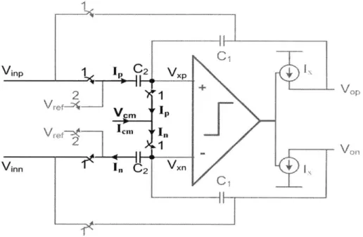
Zero-Crossing Detector
Zero-crossing detector replaces the opamp in opamp-based circuits to detect the vir-tual ground condition. When it detects, zero-crossing detector turns off the sampling switches of the next stage and the output current sources in its own stage. The schematic of zero-crossing detector is shown in Figure 3-12 [24]. The first stage con-sists of a differential amplifier and the second stage is a dynamic inverter [28]. Its operation is based on the fact that V,, is pre-charged to a voltage larger than the virtual ground and ramps down linearly, and Vi,, is pre-discharged to a voltage less
than the virtual ground and ramps up linearly. When /,p is high and Vi, is low, V1
is high. As V,, ramps down and Vi,,n ramps up, the voltage at V1 starts to reduce.
The second stage monitors V1 and when it passes the threshold voltage of transistor
the detection starts. When V0st is low, the current source of the first stage turns off
to save power. It turns on before the next detection starts. In the first stage, the active load is binary-weighted and programmable to adjust the offset of the detector. Offset of the zero-crossing detector is mainly due to the mismatch of the transistors in its first stage. Process variation also affects the threshold voltage of the second stage of the zero-crossing detector. The offset of the zero-crossing detector causes an overshoot at the output voltage. In other words, the offset of the zero-crossing detector causes an offset at the output voltage. Table 3.2 shows some of the possible offset adjustments. When a binary-weighted load is connected, it is shown by code
1, and when it is disconnected, it is shown by code 0.
First Stage
Second Stage
Enb - -Enb
Vo1 M21 M21 Vcont
Vinp -[ |-Vinn Enb
-Vo2
Iref
Figure 3-12: Schematic of zero-crossing detector.
3.2.4
Current Sources
In an ADC configuration, the output voltage is sampled by the sampling switches. After the output of a stage is sampled, the voltage on its sampling capacitors and feedback capacitors are not needed any longer. In comparison, in a filter configura-tion, since each stage is integrating its inputs, the current voltage of the integrating