HAL Id: tel-03221346
https://hal.archives-ouvertes.fr/tel-03221346
Submitted on 8 May 2021HAL is a multi-disciplinary open access
archive for the deposit and dissemination of sci-entific research documents, whether they are pub-lished or not. The documents may come from teaching and research institutions in France or abroad, or from public or private research centers.
L’archive ouverte pluridisciplinaire HAL, est destinée au dépôt et à la diffusion de documents scientifiques de niveau recherche, publiés ou non, émanant des établissements d’enseignement et de recherche français ou étrangers, des laboratoires publics ou privés.
applications: photodetectors and light emitting diodes
Junling Qu
To cite this version:
Junling Qu. Colloidal semiconductor nanocrystals for optoelectronic applications: photodetectors and light emitting diodes. Material chemistry. Sorbonne Université, 2021. English. �tel-03221346�
Spécialité: Physique et chimie des Matériaux
École doctorale 397
Réalisée à l’Institut des NanoSciences de Paris (INSP)
Présentée par Junling QU
Pour obtenir le grade de docteur de SORBONNE UNIVERSITÉ
Sujet de la thèse
Nanocristaux colloidaux pour l’optelectronique, application
aux Diodes électroluminescentes et à la détection
Soutenue le 29 avril 2021
Devant le jury composé de
Dr. Dmitry Aldakov
Dr. Lionel Hirsch
Prof. Bruno Masenelli
Prof. Davy Gérard
Prof. Corinne Chanéac
Dr. Emmanuel Lhuillier
Rapporteur
Rapporteur
Examinateur
Examinateur
Examinatrice
Directeur de thése
CEA Grenoble
Université de Bordeaux
INSA Lyon
UTT Troyes
Sorbonne université
INSP
3
I.1 Colloidal semiconductor nanocrystals ... 18
I.2 The transport and doping of colloidal nanocrystal arrays ... 26
II.1 Introduction to nanocrystal-based infrared photodetection ... 32
II.2 Ag2Se nanocrystals for mid-infrared photodetection ... 38
II.3 Degenerately doped ITO nanocrystals for mid-infrared detection ... 51
Table of contents
Notations and abbreviations ... 5
Acknowledgements ... 9
General introduction ... 11
Publications and conferences ... 13
Part I Introduction to colloidal nanocrystals ... 17
I.1.1 Quantum confinement effect ... 18
I.1.2 Hot injection synthesis of colloidal nanocrystals ... 20
I.1.3 Ligands of nanocrystals ... 22
I.1.4 Heterostructure of nanocrystals... 22
I.1.5 Shape control of Nanocrystals ... 24
I.2.1 The hopping transport in nanocrystal solids and ligand exchange ... 26
I.2.2 Field effect transistor ... 27
I.2.3 X-ray photoemission to build energy diagrams of nanocrystal arrays ... 29
Part II Heavy-metal-free nanocrystals for mid-infrared photodetection ... 31
II.1.1 Infrared photodetection ... 32
II.1.2 Photoconductors and photodiodes ... 33
II.1.3 Figures of merit for infrared photodetection... 34
II.1.4 Infrared-active nanocrystals ... 35
II.1.5 The state-of-the-art of nanocrystal-based photodetectors ... 36
II.1.6 Challenges of nanocrystal based infrared photodetectors ... 37
II.2.1 Tunable mid-infrared intraband transitions of Ag2Se ... 38
II.2.2 The origin of doping for Ag2Se nanocrystals ... 42
II.2.3 Transport properties of Ag2Se nanocrystal arrays in dark conditions ... 44
II.2.4 Photoconductance of Ag2Se nanocrystal arrays ... 47
4
III.1 Introduction to nanocrystal light emitters ... 66
III.2 Nanoplatelet-based LEDs for all-nanocrystal LiFi-like communication ... 73
III.3 HgTe nanocrystals for infrared electroluminescence and active imaging ... 92
II.3.2 Synthesis and optical properties of ITO nanocrystals ... 53
II.3.3 Transport properties of ITO nanocrystals ... 57
II.3.4 Photoconductance in ITO nanocrystal films ... 59
II.3.5 Conclusions and perspectives ... 63
Part III Nanocrystal-based LEDs and their applications ... 65
III.1.1 Colloidal nanocrystals for display with large gamut ... 66
III.1.2 Nanocrystals as down converters for QD-LCD display ... 67
III.1.3 QLED for future display ... 67
III.1.4 Nanocrystal-based LEDs beyond QD and visible ... 72
III.2.1 Synthesis and characterization of CdSe/CdZnS NPLs ... 75
III.2.2 Fabrication and characterization of NPL based LED ... 78
III.2.3 Characterization of the LED devices based on different CdSe/CdZnS NPLs ... 79
III.2.4 The origin of efficiency droop: beyond Auger recombination in emitting layer .. 85
III.2.5 Toward all-nanocrystal-based LiFi-like communication ... 87
III.2.6 Conclusions and perspectives ... 91
III.3.1 The design of the new-generation HgTe nanocrystal-based LED ... 94
III.3.2 Synthesis and characterization of the building-block nanocrystals ... 95
III.3.3 The investigation of HgTe/ZnO heterojunction as light emitter ... 100
III.3.4 Fabrication and characterization of the SWIR HgTe based LEDs ... 104
III.3.5 Toward narrower and brighter LED using sphere HgTe seeds ... 109
III.3.6 Conclusions and perspectives ... 112
General conclusion and perspectives ... 113
5
Notations and abbreviations
Physical constants
Symbol value description
ⅇ 1.60910-19 C Electron charge
𝑐 299792458 m/s Speed of light
ℎ 6.6210-34 Js Plank constant
ℏ 1.0510-34 Js Reduced plank constant
𝑚0 9.1110-31 kg Free electron mass
𝜖0 8.8510-12 kg-1m-3s4A2 Vacuum permittivity
Abbreviations
Abbreviation Description
NC(s) Nanocrystal(s)
QD, CQD Quantum dot, colloidal quantum dot
QW, CQW Quantum well, colloidal quantum well
DOS Density of states
NPL Nanoplatelet
FET Field effect transistor
XPS, UPS X-ray photoemission spectroscopy
XRD X-ray diffraction
EDX Energy-dispersive X-ray spectroscopy
RBS Rutherford Backscattering Spectrometry
SEC spectroelectrochemistry
TEM Transmission electron microscopy
FTIR Fourier-transform infrared spectroscopy
CB, VB Conduction band, valance band
LOMO Lowest occupied molecular orbital
HOMO Highest occupied molecular orbital
UV Ultraviolet
IR, NIR Infrared, near infrared
SWIR Short-wave infrared
MWIR Mid-wave infrared
6
Abbreviation Description
QCL Quantum cascade laser
c-ALD Colloidal-atomic layer deposition
Ag2Se, t-Ag2Se Silver selenide, tetragonal silver selenide
ITO Indium tin oxide
AZO Aluminum doped zinc oxide
LSPR Localized surface plasmonic resonance
LED Light emitting diodes
QD-LED Quantum dot light emitting diode
OLED Organic light emitting diode
LCD Liquid crystal display
QD-LCD quantum dot enhanced LCD
TCO Transparent conductive oxides
CTL Charge transport layer
ETL Electron transport layer
HTL Hole transport layer
Au gold
Ag Silver
EQE External quantum efficiency
IQE Internal quantum efficiency
PL Photoluminescence
PLQY Photoluminescence quantum yield
EL Electroluminescence
Li-Fi Light Fidelity
PEDOT:PSS poly(3,4-ethylenedioxythiophene) polystyrene sulfonate Poly-TPD Poly(N,N'-bis-4-butylphenyl-N,N'-bisphenyl)benzidine PVK Poly(9-vinyl) carbazole EDT Ethanedithiol
7
Notations
Notation Description
T Temperature
ℎ𝜈 Photon energy
𝑚𝑒∗ Effective mass of electrons
𝑚ℎ∗ Effective mass of holes
𝑚𝑒ℎ∗ Reduced mass of electron/hole pair
𝜖𝑟 Dielectric constant of the semiconductor
𝜖∞ High frequency dielectric constant
𝑎0 Excitonic Bohr radius
𝑘 Wave vector
𝜙𝑛,𝐿 n
th root of the spherical Bessel function of the Lth order
𝐸𝑔 Band gap energy
𝐸𝐶 Confinement energy
EF Fermi level
WF Work function
1 Se The first energy level of the conduction band
1 Sh The first energy level of the valence band
1 Pe The second energy level of the conduction band
𝛼 Absorption coefficient
𝜎 Absorption cross-section
𝐼𝑙𝑖𝑔ℎ𝑡 Light current
𝐼𝑑𝑎𝑟𝑘 Dark current
𝑃𝑖𝑛𝑐 Incident photon energy
𝑉𝐺𝑆 Gate bias in a field effect transistor
9
Acknowledgements
At the end of this PhD journey, I am so glad that I have survived while enjoyed it. I owe this unexpectedly rich experience to all the wonderful people I have met during the last several years, and here I would like to express my sincere gratitude to them.
First, I would like to thank the members of the jury: Corinne Chanéac, Dmitry Aldakov, Lionel Hirsch, Bruno Masenelli, and Davy Gérard, for reviewing my manuscript and proposing provoking discussions during the defense.
My special thanks go to my supervisor Emmanuel Lhuillier. It is fun to think about the process we became supervisor and student. I was then an aimless master student who was trying to find a host group in Paris for CSC application, not knowing what to expect. It almost shocked me when I got a reply in half an hour asking for further details. I guess we were like a blind box for each other in the beginning, but I believe it have worked out great. During the last three years and half, I have continuously been impressed by your passion for science, your sharp sense for the reaerch field, and your magic skills to make the team running, even at the worst situations. As a student, I have benefited a lot from your previsional yet explicit organizations throughout the course of the PhD. Above all, thank you for offering me the opportunity to work in the amazing OCN team, where I have never stopped absorbing knowledge and growing in so many aspects.
I then wish to thank my colleagues from the OCN team of INSP. Specially, I want to express my gratitude to Nicolas Goubet for introducing me to nanocrystal synthesis, on which I had zero experience and knowledge before. But more importantly, you gave me the wise advices such as “you have to find a way to work” and “try to collect some data everyday”, which really helped me to go through the PhD years. Clément, it was so lucky of me to have your warm help when I joined the team. You have taught me so many stuffs and I am still using the little “livachian” tools you introduced me. Please stop breaking yourself, and I expect that we will meet again! Bertille has always been a wonderful teacher to me. I could always get clear explanations for whatever I did not understand, without feeling stupid of myself. How lucky your students are! Charlie has always amazed me with resourcefulness and open creative mind. Thank you for being so helpful for keeping the equipment working. I indeed agree that, Charlie should not be the first solution to all the problems: ) Audrey, to me you are like a super girl full of energy. Cannot thank you more for being so kind and caring to me. You will do a great job on whatever you will take, with your passion, determination, and brilliance. Prachi, I have really appreciated the quality time we spent together in and out of the lab. I will remember the walks in the rains and snows (coincidence?), the festival of light, and your super tasty home cooking. I wish all the best for you in life and career. I also wish to thank Amardeep and Julien, the former postdocs of the team, for their help in experiments and fun conversations. Adrien and Tung, keep good work and wait for the day of opening. Erwan and Corentin, you are super great students, and it is such a pleasant experience to work with you! I kind of think that I have learned more from you than what I had taught you. Mariarosa, I hope you have enjoyed here.
I also wish to thank the colleagues from the LPEM lab of ESPCI. I am very grateful for Sandrine Ithurria for being so nice, warm, cheerful, and always ready to help. I am also extremely lucky to have met Xiangzhen Xu in the beginning of the PhD, for exhaustive explanations on TEM, and additionally, relaxing chats on familiar topics, which is definitely precious when I am 8000 km away from home. For a similar reason, I want to thank Ye Jiang for company and introducing me the Chinese friends and restaurants around the lab when I just arrived. I also appreciate the friendly help and interesting communications with Marion Dufour, Eva Izquierdo, and Mannon Debayle, as well as the “new” PhD students, Nicolas Moghaddam and Sobha Jana, with whom I had great time during the Germany summer school in 2019.
10
During my PhD in INSP, I have received a lot of assistance from Hérve Cruguel during synchrotron runs and XPS measurements, Yoann Prado for nanocrystal synthesis, as well as Erwan Dandeu and Loïc Becerra for their help during cleanroom fabrication.
I also want to express my thanks to the collaborators during my PhD projects: Xavier Marie, Delphine Lagarde, and Cédric Robert from INSA Toulouse for time-resolved PL measurements, Gilles Patriarche from C2N for STEM images, Simon Ferré from New Image Technology for active imaging, and Mathieu Silly from the Tempo beamline of Soleil for his assistance with all these runs. Their expertise had greatly enriched my PhD work.
There are also so many kind people who have made my stay in France much easier and delightful. I would like always thank Alain Dubois, my friend since 2013. Actually, it was the internship in LCPMR in 2014 that had initiated my motivation to go back to Paris for PhD. Thank you so much for taking care of all the NPU students in Paris. I am also deeply grateful for your checking my situation on a daily basis during the first Covid confinement. See you soon in Xi’an! My thanks also go to my friends in Paris, Bing Ma, Baojie Li, Xingyu Yang and Lingfei Cui, Kai Zhang, Jiawen Liu... for their time, support and advices, especially during the last period of my PhD. I would also like to express my appreciation to the administrative staffs of CSC and the education department of the Chinese embassy, for their super efficient organization and fast feedback. Before going to the end, I want to thank my family for their continuous support and love. I am eventually going home, so I guess mother can stop worrying soon.
I reserve my last appreciation for Jiaping Zhang, my dearest friend and firmest ally. You are always my shell that protects and passivates me. The two years we spent in Paris will definitely be one of the highlight times in our memory. Now, I am so happy that I will join you to start our new phase of life, after too long a separation.
11
General introduction
Semiconductors lie in the center of electronics and optoelectronics that have founded the information age we are living in. The growing demands for smarter devices in all walks of life, including information, communication, sensing, entertainment, therapy, and energy harvesting, has spurred the revolution of semiconductors toward by-design tailored chemical-physical properties and compatibility with new manufacturing technologies targeting low-cost, large-area, flexible and wearable devices.
Quantum engineering, which tailors the electronic properties of semiconductors for specific applications, is proposed back in the 60s of the last century. Thanks to the development of molecular beam epitaxial (MBE) technique that allows atom-by-atom deposition of semiconductors, 2D quantum wells was first obtained, followed by the discovery of epitaxially grown 1D quantum rods and 0D quantum dots (QDs). The first QDs obtained were small islands of InAs on the GaAs substrates induced by a large lattice mismatch.1 The semiconductors with one or more dimensions in the nanoscale exhibit size-dependent electronic and optoelectronic properties due to quantum confinement. On-demand properties as they can provide, the epitaxial growth is limited to niche applications such as defense and research, due to their high cost (comes with high-vacuum equipment), selective range of suitable materials and substrates, and compatibility with only the rigid and planar devices.
The emergence of colloidal nanocrystals has opened new opportunities for quantum engineering at low cost and with solution-processibility. In 1993, Bawendi’s group synthesized the first monodispersed II-VI semiconductor QDs using wet-chemistry2. Since then, in a short time, the community has been developed the synthesis to grow nanocrystals with fine control over size, shape,3,4 composition, and even heterostructures5 analogy to traditional semiconductors. These chemically synthesized nanocrystals are featured with an inorganic semiconductor core (2 to 20 nm) capped by organic molecule ligands (typically alkane chain with 12-18 carbons). The inorganic core, as a single-crystal fragment of corresponding bulk materials, can provide size-tunable properties, whereas the organic ligands allow for their dispersion in solvents, hence compatibility to solution-processed deposition technologies for rigid or flexible substrates. Combining the advantages of inorganic and organic materials, colloidal nanocrystals is regarded as the most interesting building block for the next generation of optoelectronics such as light emission, sensing, and harvesting.
After more than two decades of development, colloidal nanocrystals achieved their first commercialization when Sony released their BRAVIA QDTV in 2013 using the QDs from QD Vision, Inc., after which Samsung followed suit. Although it is only a manifestation of the high color purity and photostability of QDs, it has encouraged their integration into practical consumer devices. There are two domains of optoelectronic applications where the colloidal nanocrystals are particularly interesting.
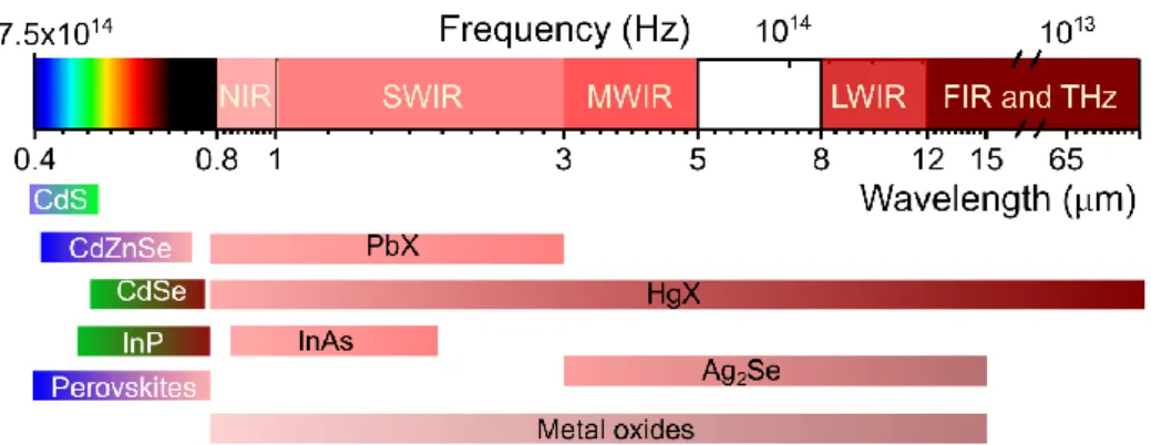
One is for infrared photodetection. In the wavelength above 1 µm, Si-based photodetectors which combines good performance and extremly low price, is not operative, neither the organic electronics, the low-cost alternative to Si electronics. At present, the infrared photodetection is dominated by epitaxially grown quantum wells6 and type II superlattice7 or narrow band gap semiconductors such as InSb and mercury cadmium telluride (MCT).8 The cost rupture required for civilian-oriented quantum photodetectors, is most likely from colloidal nanocrystals derived from narrow-bandgap semiconductors and semimetals. PbS nanocrystals, for example, are already commercially available for SWIR cameras.9 The photodetectors for longer wavelength in the infrared (above 3 µm) is being addressed by mercury chalcogenides featuring the widest optical absorptions from visible to THz. However, the heavy metals such as lead and mercury
12
have raised a toxicological concern to the mass market10, and the searching and evaluation of heavy-metal-free nanocrystals is extremely essential.
Another important playground for colloidal nanocrystals is light emitting diodes. The narrow emission linewidth of nanocrystals makes them promising candidates for large gamut displays. With the development of core/shell heterostructure nanocrystals with near-unity PLQY and enhanced stability, the QD-based LEDs of three primary colors, have achieved the EQE close to the theoretical upper limit (>20%), and high brightness on par with commercially available organic LEDs.
In this context, my PhD conducted at INSP under the supervision of Dr. Emmanuel Lhuillier, is focused on the colloidal nanocrystal-based infrared photodetectors and light emitting diodes. During my PhD, benefiting from this topic at the interface of chemistry and physics, I have developed knowledge and skills of the synthesis of various nanocrystals, clean room fabrication, and the optical and electrical characterization of the fabricated devices.
Organization of the manuscript:
Part I is a general introduction to colloidal nanocrystals. It starts with the size and dimension dependence of optoelectronic properties of nanocrystals. Then, it advances to the synthetic approach of colloidal nanocrystals and their development towards different shape and heterostructures. Then, I will switch to the electronic perspective and focus on the transport and doping of the nanocrystal arrays, which are essential for their device integration. I will introduce the techniques to determine the doping and the electronic spectrum of the nanocrystal arrays.
Part II and Part III will be dedicated to nanocrystal-based photodetectors and light emitting diodes, respectively.
Part II will begin with an introduction to the infrared photodetection, after which the results of two heavy-metal-free nanocrystals for infrared detection will be presented. The first material is self-doped silver selenide (Ag2Se) nanocrystals with size-tunable mid-infrared absorption thanks to intraband transition. The second material is tin doped indium oxide (ITO) nanocrystals with widely tunable infrared absorption raised by plasmonic resonance, whose energy is defined remotely by the tin dopants in the nanocrystals. For both heavy-metal-free material systems, I start by synthesizing the materials. Then, I probe their electronic properties including the doping and band alignment in the form of a nanocrystal array. Last, I put the nanocrystals into a photoconductive device and evaluate their capacity of infrared detection. Part III of this thesis will begin with an introduction to the application of nanocrystals as light emitters, with an emphasis on the light emitting diodes. In the following I will first present the core/shell nanoplatelets (NPLs) as emitting layer for visible LEDs. The synthesis of NPLs, the design and fabrication of the LED device will be introduced, and the characterization of the LED performance will be presented. Specially, by applying a low temperature strategy at the whole device level, we investigate the origin of efficiency roll-off, which is a common problem faced by all LEDs. Last, we build the first all-nanocrystal-based Li-Fi like communication setup with home-made LED and PbS photodetector. Then I will focus on the use of HgTe nanocrystal
emitter for LEDs emitting in the short-wave infrared. I will introduce the design of the
all-nanocrystal LED structure, the synthesis and characterization of the constituting all-nanocrystal layers, and the fabrication and characterization of the LED devices. Two types of HgTe nanocrystals from different synthetic routes are tested in this device stack. The bright home-made HgTe LED is demonstrated to be capable of active imaging as light source.
13
Publications and conferences
Pbulications
2021
1. Y. Prado, J. Qu, C. Gréboval, C. Dabard, P. Rastogi, A. Chu, A. Khalili, X. Z. Xu, C. Delerue, S. Ithurria, and E. Lhuillier, Seeded Growth of HgTe Nanocrystals for Shape Control and Their Use in Narrow Infrared Electroluminescence, Chem. Mater. 33, 2054 (2021). 2. C. Gréboval, A. Chu, D. V. Magalhaes, J. Ramade, J. Qu, P. Rastogi, A. Khalili, S.-S. Chee,
H. Aubin, G. Vincent, S. Bals, C. Delerue, and E. Lhuillier, Ferroelectric Gating of Narrow Band-Gap Nanocrystal Arrays with Enhanced Light–Matter Coupling, ACS Photonics 8, 259 (2021).
3. P. Rastogi, A. Chu, T. H. Dang, Y. Prado, C. Gréboval, J. Qu, C. Dabard, A. Khalili, E. Dandeu, B. Fix, X. Z. Xu, S. Ithurria, G. Vincent, B. Gallas, and E. Lhuillier, Complex Optical Index of HgTe Nanocrystal Infrared Thin Films and Its Use for Short Wave Infrared Photodiode Design, Advanced Optical Materials 2002066 (2021).
2020
4. J. Qu, P. Rastogi, C. Gréboval, C. Livache, M. Dufour, A. Chu, S.-S. Chee, J. Ramade, X. Z. Xu, S. Ithurria, and E. Lhuillier, Nanoplatelet-Based Light-Emitting Diode and Its Use in
All-Nanocrystal LiFi-like Communication, ACS Appl. Mater. Interfaces 12, 22058 (2020).
5. J. Qu, P. Rastogi, C. Gréboval, D. Lagarde, A. Chu, C. Dabard, A. Khalili, H. Cruguel, C. Robert, X. Z. Xu, S. Ithurria, M. G. Silly, S. Ferré, X. Marie, and E. Lhuillier,
Electroluminescence from HgTe Nanocrystals and Its Use for Active Imaging, Nano Lett.
20, 6185 (2020).
6. C. Gréboval, P. Rastogi, J. Qu, A. Chu, J. Ramade, A. Khalili, C. Dabard, T. H. Dang, H. Cruguel, A. Ouerghi, N. Witkowski, M. G. Silly, and E. Lhuillier, Time-Resolved
Photoemission to Unveil Electronic Coupling between Absorbing and Transport Layers in a Quantum Dot-Based Solar Cell, J. Phys. Chem. C 124, 23400 (2020).
7. N. Moghaddam, C. Gréboval, J. Qu, A. Chu, P. Rastogi, C. Livache, A. Khalili, X. Z. Xu, B. Baptiste, S. Klotz, G. Fishman, F. Capitani, S. Ithurria, S. Sauvage, and E. Lhuillier, The
Strong Confinement Regime in HgTe Two-Dimensional Nanoplatelets, J. Phys. Chem. C
124, 23460 (2020).
8. J. Ramade, J. Qu, A. Chu, C. Gréboval, C. Livache, N. Goubet, B. Martinez, G. Vincent, and E. Lhuillier, Potential of Colloidal Quantum Dot Based Solar Cells for Near-Infrared
Active Detection, ACS Photonics 7, 272 (2020).
9. P. Rastogi, A. Chu, C. Gréboval, J. Qu, U. N. Noumbé, S.-S. Chee, M. Goyal, A. Khalili, X. Z. Xu, H. Cruguel, S. Ithurria, B. Gallas, J.-F. Dayen, L. Dudy, M. G. Silly, G. Patriarche, A. Degiron, G. Vincent, and E. Lhuillier, Pushing Absorption of Perovskite Nanocrystals
into the Infrared, Nano Lett. 20, 3999 (2020).
10. D. Amelot, P. Rastogi, B. Martinez, C. Gréboval, C. Livache, F. A. Bresciani, J. Qu, A. Chu, M. Goyal, S.-S. Chee, N. Casaretto, X. Z. Xu, C. Méthivier, H. Cruguel, A. Ouerghi, A.
14
Nag, M. G. Silly, N. Witkowski, and E. Lhuillier, Revealing the Band Structure of FAPI
Quantum Dot Film and Its Interfaces with Electron and Hole Transport Layer Using Time Resolved Photoemission, J. Phys. Chem. C 124, 3873 (2020).
11. N. Goubet, M. Thomas, C. Gréboval, A. Chu, J. Qu, P. Rastogi, S.-S. Chee, M. Goyal, Y. Zhang, X. Z. Xu, G. Cabailh, S. Ithurria, and E. Lhuillier, Near- to Long-Wave-Infrared
Mercury Chalcogenide Nanocrystals from Liquid Mercury, J. Phys. Chem. C 124, 8423
(2020).
2019
12. J. Qu, C. Livache, B. Martinez, C. Gréboval, A. Chu, E. Meriggio, J. Ramade, H. Cruguel, X. Z. Xu, A. Proust, F. Volatron, G. Cabailh, N. Goubet, and E. Lhuillier, Transport in ITO
Nanocrystals with Short- to Long-Wave Infrared Absorption for Heavy-Metal-Free Infrared Photodetection, ACS Appl. Nano Mater. 2, 1621 (2019).
13. M. Dufour, J. Qu, C. Greboval, C. Méthivier, E. Lhuillier, and S. Ithurria, Halide Ligands
To Release Strain in Cadmium Chalcogenide Nanoplatelets and Achieve High Brightness,
ACS Nano 13, 5326 (2019).
14. C. Livache, B. Martinez, N. Goubet, C. Gréboval, J. Qu, A. Chu, S. Royer, S. Ithurria, M. G. Silly, B. Dubertret, and E. Lhuillier, A Colloidal Quantum Dot Infrared Photodetector
and Its Use for Intraband Detection, Nature Communications 10, 2125 (2019).
15. C. Livache, N. Goubet, C. Gréboval, B. Martinez, J. Ramade, J. Qu, A. Triboulin, H. Cruguel, B. Baptiste, S. Klotz, G. Fishman, S. Sauvage, F. Capitani, and E. Lhuillier, Effect
of Pressure on Interband and Intraband Transition of Mercury Chalcogenide Quantum Dots, J. Phys. Chem. C 123, 13122 (2019).
16. B. Martinez, R. Plamont, C. Gréboval, P. Rastogi, Y. Prado, J. Qu, A. Chu, C. Livache, X. Z. Xu, H. Cruguel, S. Ithurria, M. G. Silly, N. Goubet, and E. Lhuillier, Azobenzenes as
Light-Activable Carrier Density Switches in Nanocrystals, J. Phys. Chem. C 123, 27257
(2019).
17. B. Martinez, J. Ramade, C. Livache, N. Goubet, A. Chu, C. Gréboval, J. Qu, W. L. Watkins, L. Becerra, E. Dandeu, J. L. Fave, C. Méthivier, E. Lacaze, and E. Lhuillier, HgTe
Nanocrystal Inks for Extended Short-Wave Infrared Detection, Advanced Optical
Materials 7, 1900348 (2019).
18. C. Gréboval, U. Noumbe, N. Goubet, C. Livache, J. Ramade, J. Qu, A. Chu, B. Martinez, Y. Prado, S. Ithurria, A. Ouerghi, H. Aubin, J.-F. Dayen, and E. Lhuillier, Field-Effect
Transistor and Phototransistor of Narrow-Band-Gap Nanocrystal Arrays Using Ionic Glasses, Nano Lett. 19, 3981 (2019).
19. C. Gréboval, E. Izquierdo, C. Livache, B. Martinez, M. Dufour, N. Goubet, N. Moghaddam,
J. Qu, A. Chu, J. Ramade, H. Aubin, H. Cruguel, M. Silly, E. Lhuillier, and S. Ithurria,
Impact of Dimensionality and Confinement on the Electronic Properties of Mercury Chalcogenide Nanocrystals, Nanoscale 11, 3905 (2019).
20. Chu, C. Gréboval, N. Goubet, B. Martinez, C. Livache, J. Qu, P. Rastogi, F. A. Bresciani, Y. Prado, S. Suffit, S. Ithurria, G. Vincent, and E. Lhuillier, Near Unity Absorption in
15
Nanocrystal Based Short Wave Infrared Photodetectors Using Guided Mode Resonators,
ACS Photonics 6, 2553 (2019).
21. Chu, C. Gréboval, N. Goubet, B. Martinez, C. Livache, J. Qu, P. Rastogi, F. A. Bresciani, Y. Prado, S. Suffit, S. Ithurria, G. Vincent, and E. Lhuillier, Near Unity Absorption in
Nanocrystal Based Short Wave Infrared Photodetectors Using Guided Mode Resonators,
ACS Photonics 6, 2553 (2019).
2018
22. J. Qu, N. Goubet, C. Livache, B. Martinez, D. Amelot, C. Gréboval, A. Chu, J. Ramade, H. Cruguel, S. Ithurria, M. G. Silly, and E. Lhuillier, Intraband Mid-Infrared Transitions in
Ag2Se Nanocrystals: Potential and Limitations for Hg-Free Low-Cost Photodetection, The
Journal of Physical Chemistry C 122, 18161 (2018).
23.C. Livache, N. Goubet, B. Martinez, A. Jagtap, J. Qu, S. Ithurria, M. G. Silly, B. Dubertret, and E. Lhuillier, Band Edge Dynamics and Multiexciton Generation in Narrow Band Gap
HgTe Nanocrystals, ACS Appl. Mater. Interfaces 10, 11880 (2018).
24. A. Jagtap, N. Goubet, C. Livache, A. Chu, B. Martinez, C. Gréboval, J. Qu, E. Dandeu, L. Becerra, N. Witkowski, S. Ithurria, F. Mathevet, M. G. Silly, B. Dubertret, and E. Lhuillier,
Short Wave Infrared Devices Based on HgTe Nanocrystals with Air Stable Performances,
J. Phys. Chem. C 122, 14979 (2018).
25. A. Jagtap, C. Livache, B. Martinez, J. Qu, A. Chu, C. Gréboval, N. Goubet, and E. Lhuillier,
Emergence of Intraband Transitions in Colloidal Nanocrystals, Opt. Mater. Express, 8,
1174 (2018).
Conferences
1. Conference: Nanax 9, 16-20 September, 2019, Hamburg, Germany (Poster)
2. Summer school: Exciting nanostructures, 21-26 July, 2019, Bad Honnef, Germany (Poster) 3. Summer school: Physical and chemical principles in materials science, 09-15 July, 2018,
17
Part I Introduction to colloidal nanocrystals
I.1 Colloidal semiconductor nanocrystals……….……….18
I.1.1 Quantum confinement effect………..18
I.1.2 Hot injection synthesis of colloidal nanocrystals………20
I.1.3 Ligands of nanocrystals………..22
I.1.4 Heterostructure of nanocrystals……….22
I.1.5 Shape control of Nanocrystals………..24
I.2 The transport and doping of colloidal nanocrystal arrays……….…….…….……26
I.2.1 The hopping transport in nanocrystal solids and ligand exchange……….….….….26
I.2.1 The hopping transport in nanocrystal solids and ligand exchange……….…..…….26
I.2.2 Field effect transistor ……….……….………27
18
I.1
Colloidal semiconductor nanocrystals
I.1.1 Quantum confinement effect
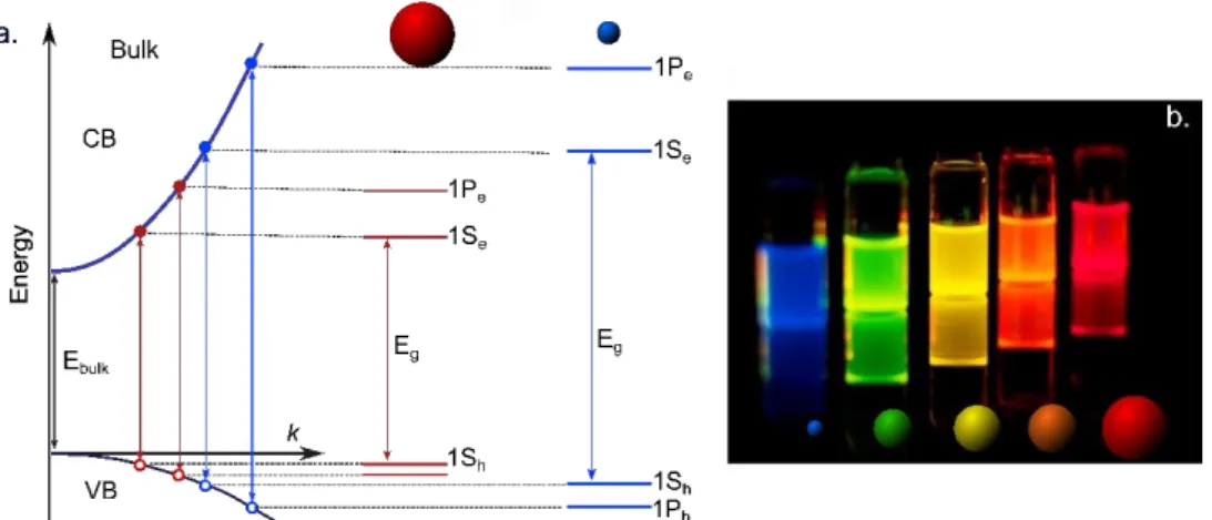
In a semiconductor, when an electron in the valance band (VB) is excited by a photon with an energy higher than that of the bandgap, the electron can be promoted to the conduction band (CB), leaving a hole in the VB. The formed electron/hole pair, bonded with electrostatic interaction, is called an exciton. The average distance of the electron/hole pair is defined as excitonic Bohr radius, which is given as:
𝑎0=
4𝜋𝜖0𝜖𝑟ℏ2 𝑚0𝑚𝑒ℎ∗ ⅇ2
(I-1)
Where 𝜖0 is the permittivity of the free space, 𝜖𝑟 is the dielectric constant of the semiconductor, ℏ is the reduced Plank constant, 𝑚0 is the rest mass of an electron, ⅇ is the charge of an electron, and 𝑚𝑒ℎ∗ is the reduced mass of electron/hole pair, which is calculated as:
1 𝑚𝑒ℎ∗ = 1 𝑚𝑒∗ + 1 𝑚ℎ∗ (I-2)
With 𝑚𝑒∗ and 𝑚ℎ∗ the effective mass of electrons and holes, respectively. For example, the Bohr radius is around 6 nm for CdSe, 21 nm for PbS and 40 nm for HgTe.
For strongly confined nanocrystals (quantum dots when they are sphere) whose size is close to or smaller than 𝑎0, a photo-induced exciton can be treated as a particle in a box, where the nanocrystal composition defines the effective mass and shape and size define the dimension of the box, leading to a discrete atom-like energy spectrum. The most common way to describe these discrete states is to use the effective mass approximation.11 In this model, the wavefunction in the confinement direction of the nanocrystal is approximated as a product of Bloch wavefunction and an envelope wavefunction. The Bloch wavefunction describes the carrier motion in the potential of the crystal lattice, whereas the envelope wavefunction is to describe the motion of carriers in the confinement potential.
By solving the Schrodinger equation of a band in a quantum dot with a radius of R (R≤ 𝑎0), the envelope wavefunction can be obtained, with spherical Bessel function (jL) as one of the factors. And the energies are given by:
𝐸𝑛,𝐿 =
ℏ2𝜙𝑛,𝐿2 2𝑚∗𝑅2
(I-3)
With n the principal quantum number, 𝑚∗ the effective mass of electrons or holes, and 𝜙𝑛,𝐿the nth root of the spherical Bessel function of the Lth order. Thus, the discrete energy levels can be derived from the parent bulk semiconductor (see the E-k dispersion of the bulk in Figure I.1) but with discrete wavevectors (k) in the momentum space. The allowed value of k is determined by:
𝑘 =𝜙𝑛,𝐿
𝑅 (I-4)
The quantized energy level of a quantum dot can thus be ordered in energy according to the value of 𝜙𝑛,𝐿, which is 𝜋 for 1S (n=1, L=0), 4.49 for 1P (n=1, L=1), 5.76 for 1D (n=1, L=2), etc., see Figure I.1 a to the right. The corresponding ground state energy is given as:
19 𝐸1,0=
ℏ2𝜋2 2𝑚∗𝑅2
(I-5)
Which suggests that the first conduction (1Se) and valence(1Sh) band states shifts to larger values with decreasing QD size, giving rise to the size-dependent banggap of nanocrystals:
𝐸𝑔= 𝐸𝑔,𝑏𝑢𝑙𝑘+ ℏ2𝜋2 2𝑚𝑒∗𝑅2 + ℏ 2𝜋2 2𝑚ℎ∗𝑅2− 1.8 ⅇ2 𝜀∞𝑅 (I-6)
Where 𝜀∞ is the high frequency dielectric constant of the semiconductor. If we define the bandgap widening resulting quantum confinement as confinement energy 𝐸𝐶:
𝐸𝐶 = ℏ2𝜋2 2𝑚𝑒∗𝑅2 + ℏ 2𝜋2 2𝑚ℎ∗𝑅2= ℏ2𝜋2 2𝑚𝑒ℎ∗ 𝑅2 (I-7)
Then the bandgap can be interpreted as the parent bulk bandgap increased by the confinement energy (Ec) and decreased by coulombic interaction of the electrons and holes.
Figure I.1 (a) E-k dispersion relation of a bulk semiconductor (solid parabolic curves to the left) and energy levels of a spherical quantum dot of the same materials but of different sizes. (b) A picture of CdSe quantum dots in solution, with a size ranging from 6 nm to 2 nm, providing photoluminescence from red to blue due to quantum confinement.12
Figure I.1 b shows a picture of CdSe quantum dots with a size from 2 nm to 6 nm, presenting photoluminescence from blue to red, covering the whole visible range. The size-tunable emissive properties have been the most targeted function for QDs, especially for displays in the visible.
From the band gap of nanocrystals given in equation (I-7), the size-tunability of a material is determined by the effective mass of electrons and holes, or the curvature of the E-k dispersion curve. The longest wavelength (the smallest bandgap) of QD is limited by the bandgap of the bulk material, whereas the shortest wavelength (the largest band gap) is limited by the smallest size of QD we can obtain. To achieve optical features of longer wavelength such as infrared range, materials with a small bulk bandgap are required. PbS with a bulk bandgap of 0.4 eV (≈3 µm) has been widely explored in QD form for infrared photodetection and for harvesting the infrared part of solar spectrum, exploiting their tunable bandgap. Another category of material that naturally works for infrared applications is mercury chalcogenides (HgX), especially HgTe and HgSe, whose bulk bandgap is zero due to their semimetal nature. The bandgap of the quantum dots derives from HgTe and HgSe is solely controlled by the quantum confinement, which in theory can provide band gaps as small as possible.
20
Dimensionality and quantum confinement
In addition to the size, the shapes and the dimensionality of nanocrystals can also strongly influence the electronic spectrum of charge carriers as well as the optical properties of the nanocrystals. As can be seen from Figure I.2, unlike bulk semiconductors, where the density of the states (DOS) increases continuously with energy due to continuous bands, the 2D quantum well (QW) confines the motions of electrons in the thickness direction, whereas the in-plane motion of the carriers is still continuous, resulting in a staggered density of states. Quantum engineering in nanoscale was firstly realized in the epitaxially grown 2D quantum well system with electronic properties tailored to user’s specifications. Soon after, the 1D quantum wire and 0 D quantum dot was also obtained by epitaxial techniques. They confines the motion of carriers in more dimensions, bringing in further interesting optoelectronic features.
Figure I.2 The density of states of semiconductor form 3 D to 0 D dimensions. The energy density of states strongly dependent on the number of confined directions: the density of electron and hole states changes from monotonically increasing with energy in a 3 D bulk material, to the step-like quasicontinuum in 2 D quantum well, a saw-like quasicontinuum in quasi-one-dimensional nanorods and to discrete levels for zero-dimensional quantum dots.
I.1.2 Hot injection synthesis of colloidal nanocrystals
Chemically synthesized colloidal nanocrystals have become an exciting class of materials with precise control over a wide range of size, shape, and composition. The solution-processibility of colloidal nanocrystals generates tremendous technological opportunities as they can be deposited with simple methods such as spin-coating, spray-coating and dip-coating, or patterning techniques including inkjet printing and nanoimprint lithography. As a result, nanocrystals are ideal building blocks for future low-cost electronics,13 optoelectronics,14 and photonics.15
Synthesis of colloidal nanocrystals with controlled size distribution is the first step for the utilization of their size dependent properties. The milestone for the synthesis of high quality colloidal nanocrystals was achieved in the early 1990s by the group of Brus16 and Bawendi2. Using a “hot injection” method, they introduced organometallic precursors into high boiling point coordinating solvents. It was the first time when II-VI CdE (E = S, Se or Te) QDs were obtained with nearly monodisperse size and shape, and resultant sharp optical (absorption and emission) features at room temperature. This finding has set the basis for the rational synthetic schemes of colloidal nanocrystals over the past four decades.
21 (1) Degassing. The cation (or anion) precursor, ligands, and high boiling point coordinating solvent are mixed in a three-neck flask connected to Schlenk line. The mixture is kept under vacuum at an elevated temperature to remove the oxygen, water, and impurities.
(2) Hot injection. After degassing, the atmosphere is switched to an inert gas (Ar or N2) to further increase the temperature. When the temperature is stabilized at the reaction temperature, the anion (or cation) precursor is rapidly injected into the reaction bath. The nucleation is initiated upon rapid injection due to the saturation, and soon terminated due to the temperature drop after the addition of room temperature precursor. The temporal separation between nucleation and growth is thus achieved and ensures the monodisperse size and shape of the nanocrystals.
According to the target material system and size, as well as the reactivity of the precursor, the reaction temperature varies. For example, the synthesis of cadmium chalcogenides requires relatively high reaction temperature of around 250 °C, whereas for the synthesis of mercury chalcogenides, the temperature is usually below 100 °C. The size of the nanocrystal can also be tuned by the duration of reaction.
It is also worth noting that, in general, the cation precursor is injected prior to the anion precursor, whereas in some cases the sequence is reversed. For instance, during the synthesis of silver chalcogenides, the silver precursor is injected into a flask containing chalcogenides precursor. Because, in the absence of any chalcogenide, silver nanocrystals will be formed.17 (3) Quenching of the reaction. To stop the growth of the nanocrystals, excessive of ligands are generally injected into the system to avoid the precursors from accessing to the nanocrystals, and the flask is cooled by air flux or by a water or ice bath.
Figure I.3 Typical hot injection synthesis of colloidal nanocrystals including degassing of solvents and precursors, hot injection in an inert atmosphere and the quenching of reaction.
Purification of nanocrystals
To extract the nanocrystals from the reaction products, a purification process is conducted. Typically, a polar solvent such as ethanol, methanol, or acetone, is added to the reaction mixture. The change of the polarity of the solvent leads to the flocculation of the nanocrystals, leaving the excess ligands and unreacted precursors in the solvent, enabling the precipitation of nanocrystals by centrifugation. The precipitated nanocrystals are then dispersed in non-polar solvents such as hexane, toluene, or chloroform. The purification is conducted at least twice before storing the clean nanocrystals in a nonpolar solvent.
22
Figure I.4 (a) Illustration of a single CQD comprising an inorganic semiconductor core capped by an organic ligand made of long hydrocarbon molecule with a functional end anorchid to the surface of the core. (b) TEM image of CdSe/CdS quantum dots with high monodispersity.
I.1.3 Ligands of nanocrystals
A typical CQD consists of an inorganic nanocrystal core capped by long-alkyl-chain ligands, see Figure I.4 a. Figure I.4 b shows a TEM image of CdSe/CdS CQDs with a diameter of around 9 nm, revealing a high degree of monodispersity, which is mandatory to resolve the discrete energy levels of a CQD assembly and resultant optical properties.
Although the nanocrystalline core drives the target optoelectronic properties of the CQDs, their surface ligands are paid substantial attention owing to the large surface /volume ratio of nanomaterials. The commonly used ligands for colloidal nanocrystals are hydrocarbon molecules with anchoring end groups. The chain of the molecules is usually long with 12 to 18 carbons, and the end functional groups are usually thiols, amines, carboxylic acid, and phosphines. There are multiple roles played by the ligands throughout the synthesis, processing, and application:
(1) The nonpolar nature of the long alkane ligands ensures the colloidal stability of the nanocrystals in a nonpolar solvent, which is critical for solution-processable fabrication. (2) During the growth, the ligands rapidly adsorb and desorb from the surface of the growing nanocrystals, which regulate the addition and the removal of the atoms to the crystalline surface, slowing down the growth rate and in turn circumventing the aggregation and enabling fine control over the growth.3
Furthermore, some capping ligands can selectively bond to certain facets of the nanocrystals and in turn terminate the growth of the facet18. It is widely used for the synthesis of anisotropic shapes such as nanorods3 and nanoplatelets4.
(3) The capping ligand can passivate the electronic trap states induced by the dangling bonds on the QD surface, preserving the photoluminescence and exciton lifetime.
(4) The length of the ligands determines the interparticle spacing in a nanocrystal solid. The native long-chain ligand massively hindering their electrical coupling. Ligand exchange toward shorter species is needed for application-targeted high-mobility NC films.
I.1.4 Heterostructure of nanocrystals
Along with the study of the single-component nanocrystals, the synthesis of heterostructure nanocrystals, achieved by epitaxially growing an inorganic shell onto the core nanocrystal, has been developed.5,19 This is first motivated by the potential that the heterostructures, beyond single-component counterparts, can bring novel electrical and optical properties and carrier
23 behaviors. From the application point of view, the inorganic shell can better passivate the unsaturated bonds of the core nanocrystal surface than the ligands, enhancing the photoluminescence; it can also work as a physical barrier, making the optical-active core less sensitive to the environmental changes and surface chemistry. This robustness brought by shelling is critical for their integration to a device, where the materials will be inevitably exposed to harsh conditions such as strong electric field, significant heat, strong photo-irradiation and the solvents.20 All the above conditions can be challenging for single-component nanocrystals to maintain their optical properties, especially emission properties.
The carrier localization and the optoelectronic properties depend heavily on the relative position of the conduction and valence band of the core/shell nanocrystal components. Thus the core/shell nanocrystals can be categorized into type I and type II band configurations according to their band offset.11
As in a typical type I CdSe/ZnS QD, the band edge of the CdSe core is fully included in that of the ZnS shell, confining the electrons and holes in the core (Figure I.5 a), thus facilitating the radiative recombination of the excitons. Indeed, after Hines and Guyot-Sionnest published reports of ZnS-capped CdSe QDs showing luminescence up to 50% PLQY,5 considerable efforts were devoted to optimizing QD structures to achieve intense and narrow emissions 21–23, which has paved the way for the synthesis of nanocrystals with near-unity efficiency and size-tunable emission for display. It is worth noting that the lattice mismatch of the heterostructure materials should be treated carefully to avoid the interfacial defects. The common solution to release the strain and to maintain high PLQY of the heterostructure is to alloy the shell or to build a chemical gradient of core/shell materials.24
In a typical type II band alignment (Figure I.5 c), the offset of conduction bands and valence bands are of the same sign. CdTe/CdSe core/shell nanocrystals,25 for example, its electrons are localized in the shell materials with a lower conduction band while the hole wave function is restrained in the CdTe core. This spatial separation of electron and hole wave function reduces the recombination rates of the excitons, thereby prolonging the PL decay time. This type II heterostructure also allows access to optical transition energies that are not restricted to band-gap energies and can emit at lower energies than the band band-gaps of comprising materials.25 In between the carrier-localized type I and carrier-separated type II, there is a situation defined as quasi type II, where one carrier is confined in one material whereas the other can move across the entire heterostructure. This requires the conduction band or the valence band of the constituent materials close in energy. The most popular manifestation of quasi type II band alignment is CdSe/CdS nanocrystals,26 in which the holes are localized in the CdSe core and the electrons delocalizing in the two materials. This band alignment can provide high photoluminescence quantum yield as type I heterostructure for light emission. One of the interesting characterizations of this materials is that the emission red shifts with the increase of shell thickness, demonstrating the delocalization of the electrons.
Regarding the different carrier localization and the consequent interesting optical properties brought by different band alignment of the heterostructures, it is critical to engineer the core/shell materials for the design of optoelectronic devices. For example, the type I core/shell heterostructure is beneficial for high PLQY and stability required by light emission applications, whereas the type II structure can facilitate the charge carrier separation, which is preferable for photovoltaic devices and photodiodes.
24
Figure I.5 Schematic diagram of CdSe/ZnS (a), CdSe/CdS (b), and CdTe/CdSe (c) nanocrystals with type I, quasi type II, and type II band alignment, respectively. The localization of excited carriers wavefunctions are indicated.
I.1.5 Shape control of Nanocrystals
Ever since the establishment of hot injection synthesis of near-spherical CQDs, the synthesis of anisotropic nanocrystals with various shapes and dimensionality has been followed. In 2000, Peng et al. reported the first anisotropic “quantum rods” and demonstrated their directional emission.3 It was until 2008 that the zinc blende CdSe nanoplatelets (NPLs), with one dimension much smaller than the other two, was discovered, which presents extremely narrow thickness-dependent emission.27
In this part, I will focus on colloidal nanoplates, also called colloidal quantum well (CQW), as they have the electronic properties of the 2D quantum well grown by molecular beam epitaxy. Colloidal NPLs with their unique growth mechanism, allows a large lateral extension, while the confinement direction is flat with atomic precision, see the scheme of a CdSe NPL with 3 monolayers of Se atoms and 4 monolayers of Cd covering the surface in Figure I.6 a, and a TEM of CdSe NPL in Figure I.6 b. As a result, the excitons in the NPLs can move freely in the 2D plane but are strongly confined in the thickness direction (1-2 nm). For sphere QDs, their size is more or less continuous, which inevitably induces inhomogeneous broadening of the optical features, whereas the atomically flat NPL presents extremely narrow linewidth of absorption and emission (below 10 nm) due to high monodispersity. It has been reported that the linewidth of NPLs in the solution is the same as that of the single NPL, demonstrating that there is no inhomogeneous broadening of the NPL batch.28
So far, among all known nanomaterials, NPLs provide the highest color purity owing to the thickness control down to the atomic level, making them the most promising nanocrystal for high-quality light emitting applications. Moreover, the 2D structure with an in-plane 2D optical dipole can result in polarized emission, which can be harnessed to improve the extraction efficiency in a planar LED device .29,30
25 Although the single content nanoplatelets has already been interesting for light emission device, there are several drawbacks: (1) NPLs with only integral monolayers of atoms can be obtained, limiting their size-tunability in the confinement direction and consequently their emission wavelengths. (2) Like all the single component colloidal nanocrystals, the dangling bonds on the surface of NPLs generate trap states and damages their PLQY. Also, they are sensitive to the change in the environment medium and photo-oxidation and show poor optoelectronic stability, hindering their integration to operational devices.
To overcome the above-mentioned limitation, the core/shell heterostructures of NPLs have also been developed.31 Figure I.6 c and d respectively show the cartoon and the TEM image of a core/shell CdSe/CdS NPLs. It can be clearly observed that both CdSe core and ZnS shell can be grown with atom-resolved thickness, and there is a flat interface between the core and the shell, as indicated by the image contrast due to their different atomic density. In the early stage, the core/shell structure is obtained via colloidal atomic layer deposition (c-ALD) 32. In a typical c-ALD process, the cationic and anionic precursors are successively added into the reaction system. Each reaction step is self-limited by the surface binding sites, which allows the removal of excess precursors after each reaction, preventing their reaction with the following regent. In this manner, CdS shell with a thickness of up to 7 monolayers is grown on the CdSe NPLs core, emitting at 665 nm with a narrow linewidth of 20 nm.
The c-ALD approach, conducted at room temperature, can only provide core/shell NPLs with moderate PLQY (typically below 50%) and stability. The exploration of high-PLQY core/shell NPLs for high-performance light emitting devices has been continued and a breakthrough was reported in 201633 by adopting hot injection to the shell growth. CdSe/ZnS NPLs with reproducible near-unity PLQY were reported by Demir’s group in 2019.34 Soon after, the same group demonstrated a NPL-based LED with the record-high external quantum efficiency of 19.2% 35, close to what has been achieved by the QDs, although the stability of the LED device needs to be further improved.
Figure I.6 Scheme of a core-only CdSe NPL (a) and a corresponding TEM (b), adapted from the reference4. Scheme of a CdSe/CdS core/shell NPL (c) and a corresponding TEM image of CdSe/CdS core/shell NPL demonstrating atomic resolution (d), TEM adapted from the reference. 36
26
I.2 The transport and doping of colloidal nanocrystal arrays
In the preceding part, I have been focusing on the synthesis, composition, heterostructures and shape control of colloidal nanocrystals. In this part, I will emphasize the electronic properties of colloidal nanocrystals, including transport properties, doping and their energy levels in the absolute energy scale, which are critical for the design of a complex device and for the understanding of their performance.
I.2.1 The hopping transport in nanocrystal solids and ligand exchange
The emergence of high-mobility nanocrystal solids37 up to 400 cm2 V-1 s-1 has open up interesting opportunities for high-performance electronic and optoelectronic devices, such as field effect transistors (FET)38–40, photodetectors41–43, solar cells44, and light emitting diodes (LEDs)45,46. At room temperature and under an electric field, the transport of a charge carrier in a nanocrystal solid occurred through hopping from one nanocrystal to its nearest neighbor, as shown in Figure I.7 a. The mobility of the carriers in a nanocrystal array is determined by the electronic coupling strength between nanocrystals, and more directly speaking, by the hopping rate. During a hopping event, the carrier needs to overcome the tunnel barrier. As illustrated in Figure I.7 b and Figure I.7 c, the height of the tunnel barrier is controlled by the nature of the barrier material (typical value for organic ligands is probed to be 2 eV),40 while the tunnel width (d) is the inter-dot spacing (i.e., the length of ligands). In a nanocrystal solid with native ligands , the tunnel width is around 1.5 nm the typical length of alkyl chains (Figure I.7 b), which makes the nanocrystal film insulating with mobility of around 10-8 cm2 V-1 s-1. 40
To boost the conductance of the nanocrystal arrays while preserving the quantum confinement, ligand exchange of native long ligands toward shorter organic molecules or small inorganic ions47 by either solid-state method40 or solution phase transfer47 has been well established. It is reported that, in the absence of other changes, the mobility is supposed to increase exponentially with decreasing ligand length.40 To change the original long ligands with their short counterparts, the most common strategy is solid-state ligand exchange. For example, by immersing a nanocrystal films capped with long ligands into a solution of ethanethiol (EDT) in ethanol. The EDT of higher concentration will occupy the surface and replace the origin ligands. After ligand exchange towards EDT, the tunneling barrier width can be decreased to 0.3 nm (Figure I.7 c), and the mobility of the carriers improved by about 6 orders of magnitudes.40 The loss of ligand volume during this solid-state ligand exchange leads to voids in the thin film, which can be filled by multilayer deposition and exchange. It is worth noting that, for the target of light emission, the ligand species as well as the solvents for ligand exchange need to be carefully chosen to preserve the PL efficiency while enhancing the mobility.
The replacement of original ligands with compact inorganic ions such as S2- ions48 and halides44, can simultaneously reduce the tunnel barrier and height, leading to the stronger electronic coupling of the nanocrystals. Interestingly, small ions such as OH- and Cl-, helps to match the density of ligands to the number of surface atoms, in turn benefits the electronic passivation of surface dangling bonds49. For the ligand exchange toward small molecules or ions, phase-transfer ligand exchange is usually adopted. Typically, a polar solvent with the small ligands is mixed with the original nanocrystal solution. After sonication or vigorous agitation, the small molecular ligands are attached to the nanocrystal surface and bring the nanocrystal in the polar phase, whereas the original long-chain ligands are stripped from the nanocrystal and remain in the original nonpolar phase. In this phase-transfer manner, we can obtain an “ink” of nanocrystals with short ligands, which enables the deposition of thick films with good quality in one step, instead of the conventional layer-by-layer solid-state ligand exchange.
27 Figure I.7 (a) Illustration of hopping of an electron in a nanocrystals solid form one electrode to the other. (b) Cartoons of the electron hopping in a nanocrystal array with native long ligands. In this case, the hopping of an electron from one nanocrystal to another needs to overcome both a high tunneling barrier and a wide tunneling width defined by the inter-dot spacing. (c) Cartoons of an electron hopping occurred in a nanocrystal array after ligand exchange, in which the shorter ligands reduce inter-dot spacing and in turn the barrier width.
Along with the development of nanocrystal based optoelectronic devices, more complex ligand exchange strategies have been adopted. For example, the use of hybrid organic-inorganic (ammonium acetate-metal halide) inks of PbS nanocrystals has provided a nanocrystal solid with both high carrier mobility and good surface passivation, leading to high power efficiency of PbS nanocrystals-based solar cells50. In a recent report, a HgSe film with a hybrid ligand of amine/halogen and thiols using solution phase transfer demonstrates mobility of 1 cm2 V-1 s-1, two orders of magnitude higher than that of the film obtained with traditional solid-state ligand exchange using EDT solution.51
I.2.2 Field effect transistor
For the design of semiconductor optoelectronic devices, the insight of the electronic properties of the materials including doping, carrier mobility and energy levels are required. Since the Hall effect, which is commonly used in solid state physics, is not easy to conduct in a nanocrystal solid due to its low carrier mobility,52 field effect transistor (FET) has become the most straightforward way to identify their majority carrier and carrier mobility. Although FET itself
28
has been one of the target applications for the next generation of low-cost nanocrystals-based electronics, here the goal of the FET configuration is not application-oriented but rather probing the transport characteristics of the nanocrystal solids and providing insights on the nature of majority carrier, and the mobility of the carriers in a nanocrystal solid.
The most common FET configuration is shown in Figure I.8 a. In this structure, a pre-patterned metal electrode is used as drain and source, a heavily doped Si is used as the bottom gate, which is insulated from the FET channel with a thin layer of SiO2 (typically 300 nm). The channel is made of a ligand-exchanged nanocrystal film. The gating effect is illustrated in Figure I.8 b: under a certain drain-source bias, when we apply a positive gate bias (VGS>0), the positive charges will accumulate at the side of SiO2 near the nanocrystal channel, while the negative charges accumulate near the gate. To screen the positive charges near the nanocrystal film, there are electrons injected into the channel. With the same principle, if we apply a negative bias (VGS<0), holes will be injected into the nanocrystal channel.
If the majority carriers of the nanocrystal array are electrons (i.e., the nanocrystal is n-doped), the increase of gate bias in the positive range (the injection of electrons) will open the channel for the current to flow. In contrast, if the nanocrystal film has holes as its majority carriers (i.e., p-doped), the conductivity of the channel will be enhanced with more negative gate bias (the injection of holes). Under the third circumstance, the conductivity of electron and hole of the same nanocrystal film can be enhanced by the injection of electrons and holes. This kind of transport is defined as ambipolar transport.
The ability of a FET system to tune the channel carriers is determined by the capacity of the gate insulator. In this conventional dielectric back gate configuration (Figure I.8a), the capacitance (C) of the dielectric can be calculated from the formula below,
∁=𝜀0𝜀𝑟𝑆 𝑑
(I-8)
where 𝜀0 is the permittivity of free space, 𝜀𝑟 is the dielectric constant of the gate insulator, S is the surface area of the channel and d is the thickness of the dielectric layer.
The formula clearly indicates that a high capacitance can be obtained by using high dielectric materials and (or) decreasing the thickness of the dielectric layer. The capacitance of SiO2 with a thickness of 300 nm is around 10 nF/cm2, leading to a weak modulation of the charge density in the channel material. Further decreasing the thickness of SiO2 is not a practical way to increase the capacitance, as the thin dielectric layer is prone to breakdown, especially in the dielectric FET system where high bias (several tens of volt) is required to induce gate effect. Despite the the low capacity for the charge barrier injection, this FET configuration is (1) very easy to obtain, (2) compatible with fast sweep of gate bias and (3) allows for the measurement across a wide temperature range from 4 K to 300 K. A possible way to increase the capacitance can be changing the low dielectric constant SiO2 (𝜀𝑟=3.9) to high dielectric materials (high-k dielectrics), such as Al2O3 (𝜀𝑟=7.5) and HfO2 (𝜀𝑟=25).53
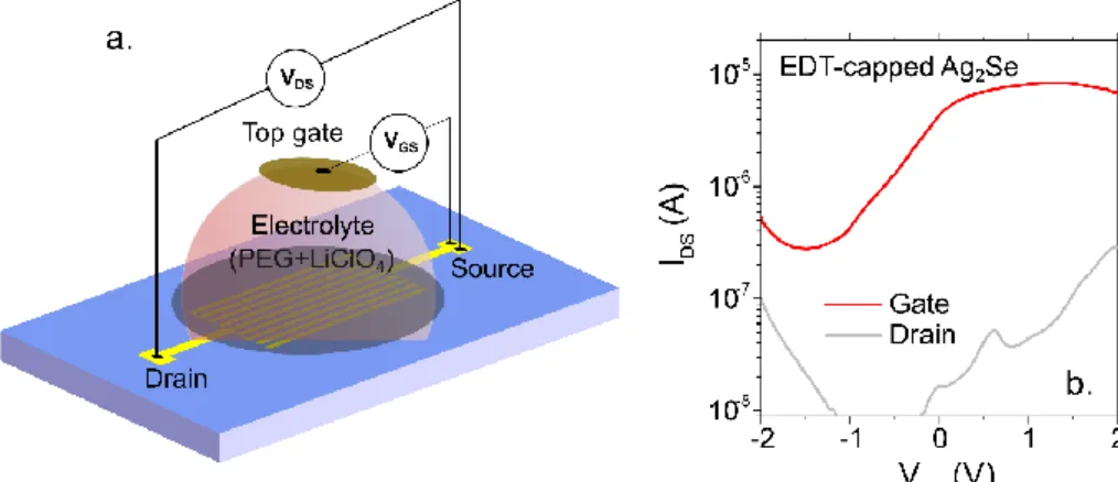
Another FET configuration routinely used in our team is an electrolyte top-gated FET. As schemed in Figure I.8 c, the same pre-patterned metal electrode is used, and the nanocrystal channel is made in the same manner as the dielectric FET configuration (Figure I.8 c). Here an electrolyte on the top of the nanocrystal channel is used for gating. The electrolyte is obtained by dissolving LiClO4 in a polymer matrix of PEG. Again, when we apply a positive gate bias (VGS>0), the ClO4- anions accumulate near the gate, whereas the mobile Li+ will migrate across the PEG matrix and diffuse deep into the nanocrystal film.
29 Figure I.8 (a) Scheme of a conventional back gate FET with SiO2 as dielectric and a heavily doped Si as gate electrode. (b) The gate effect induced in a nanocrystal film when VGS above 0 V. (c) Scheme of an electrolyte top gate FET. (d) Gate effect induced in an electrolyte gated FET when VGS above 0 V.
This electrolyte gate can powerfully tune the carrier density of the channel under low gate bias. This is owing to its capacitance in the range of µF/cm2, two orders of magnitude higher than that of the SiO2. This high capacitance makes it easier to gate higly doped nanocrystals. In addition, the ions from electrolytes can percolate deep into the nanocrystal films, enabling the gate of thick films.
However, there are several drawbacks of this FET configuration: (1) It only operates near room temperature (300 K) and fails to work below 280 K54 due to the freezing of the ions. (2) Because the injection of carriers involves the diffusion of Li+ ions in the matrix, a very slow sweep rate is required. (3) the electrochemical stability of the electrolyte limits the gate bias below 3 V. (4) It is difficult to evaluate the mobility from the transfer curve, since the precise capacitance is hard to obtain.
Nevertheless, the electrolyte is very useful to probe the nature of majority carriers, especially for heavily doped nanocrystals.
I.2.3 X-ray photoemission to build energy diagrams of nanocrystal arrays
Although FET is a useful tool to understand the doping and the mobility of the nanocrystal films, it cannot locate the absolute energy levels, such as the Fermi level, the conduction and the valence band. Knowing the relative energy levels is the prerequisite to determine contact nature (Ohmic or Schottky) of the electrode/nanocrystal and nanocrystal/nanocrystal interface, the band bending and in turn the injection of the carriers inside the device. More and more evidence has shown that the energy diagram of a nanocrystal is not only determined by the size but also hugely modified by the surface chemistry.55,56 This makes it critical to master the information of the energy diagram of all the constituting materials of a photovoltaic device57 or light emitting diodes11, to guide the design and the understanding of the device operation.
X-ray photoemission spectroscopy (XPS) is a powerful tool to probe the energy levels, determine the doping type, and reconstruct the energy spectrum of a nanocrystal film. Figure I.9 shows
30
the scheme of a XPS setup. Various light sources such as X-ray sources (K of Mg or Al), synchrotron sources and UV light (for UPS) can be used to excite the electrons from different energy levels by the photoelectric effect. Upon the X-ray incidence, the photo-generated electrons can get rid of the binding energy (BE) and escape from the sample with a kinetic energy (KE). An analyzer is used to sort the electrons according to their energy, while a detector is used to count the number of electrons of each kinetic energy. The kinetic energy of a photoelectron can be related to the binding energy according to energy conservation law: BE=h𝝂-KE, with h𝝂 the energy of the incident photon.
For the reconstruction of the energy level spectrum of nanocrystals, XPS can provide the information of the Fermi level (Ef) and relative energy of Ef and the valence band. The lowest KE of the XPS spectrum is from the electrons with just enough kinetic energy to escape from fermi level to the vacuum, that is to say, their kinetic energy is supposed to be 0 at the vacuum level. Since Ef of the detector is the same as that of the sample, the lowest kinetic energy detected is the work function value (WF) of the materials.
The lowest BE edge cutoff of XPS spectrum corresponds to the energy difference between the valence band maximum (VBM) and the Fermi level, as depicted in Figure I.9 b. Hence, we can further identify the position of the VBM using the WF value obtained from low kinetic energy cutoff. The conduction band can thus be determined by adding the bandgap (Eg) of the materials to the VBM. The bandgap of the materials is approximate by the optical spectrum.
Figure I.9 (a) A typical x-ray photoemission spectroscopy setup. The incident X-ray or ultraviolet light source can promote the electrons in the sample and the kinetic energy of the photoelectrons can be detected.
Following the method above, we can determine the energetic levels of the materials, as illustrated in Figure I.9 b. The doping of the nanocrystal film can be clearly identified by the position of the Fermi level with respect to the middle of the bandgap (Ei): when Ef is above the Ei, the materials is n-doped, when the Ef is below the Ei, the material is p-doped and when Ef is overlap with Ei, it is intrinsic. Furthermore, when the Ef located above the conduction band (1Se), the material is regarded as degenerately n doped.
During my PhD, I combine the FET and XPS techniques to understand the doping and electronic structures of the nanocrystal films that I will integrate into photodetection or light emitting device.