HAL Id: hal-03187823
https://hal.archives-ouvertes.fr/hal-03187823
Submitted on 1 Apr 2021
HAL is a multi-disciplinary open access
archive for the deposit and dissemination of
sci-entific research documents, whether they are
pub-lished or not. The documents may come from
teaching and research institutions in France or
abroad, or from public or private research centers.
L’archive ouverte pluridisciplinaire HAL, est
destinée au dépôt et à la diffusion de documents
scientifiques de niveau recherche, publiés ou non,
émanant des établissements d’enseignement et de
recherche français ou étrangers, des laboratoires
publics ou privés.
Design exploration of majority voter architectures based
on the signal probability for TMR strategy optimization
in space applications
Y Aguiar, Frédéric Wrobel, J-L Autran, P Leroux, F Saigné, V Pouget,
Antoine Touboul
To cite this version:
Y Aguiar, Frédéric Wrobel, J-L Autran, P Leroux, F Saigné, et al.. Design exploration of
ma-jority voter architectures based on the signal probability for TMR strategy optimization in space
applications. Microelectronics Reliability, Elsevier, 2020, 114, �10.1016/j.microrel.2020.113877�.
�hal-03187823�
Design Exploration of Majority Voter Architectures based on the Signal
Probability for TMR Strategy Optimization in Space Applications
Y. Q. Aguiar, F. Wrobel, J-L. Autran, P. Leroux, F. Saigné, V. Pouget and A. D. Touboul
Abstract – Hardware redundancy is a well-known fault tolerance technique used in safety- and mission-critical systems. However, the hardening efficiency of such techniques relies on the robustness of the majority voter circuitry. This summary provides the design exploration of majority voter architectures to be used in radiation environments such as in space missions. An application-specific Single-Event Transient (SET) characterization based on the signal probability is proposed to optimize the Triple-Modular Redundancy (TMR) block insertion methodologies. Results show that the SET cross-section of complex-gate architectures presents low input dependence while for the NOR/NAND based architectures a higher dependence is observed due to the logical masking effects. Additionally, different from the other architectures, the NAND voter has shown a reduction in the SET rate as the signal probability is increased. Considering the signal probability p = 0.1, p = 0.5 and p = 0.9, the best design for the two analyzed orbits is the NOR, CMOS1 and NAND voter, respectively.
1. Introduction
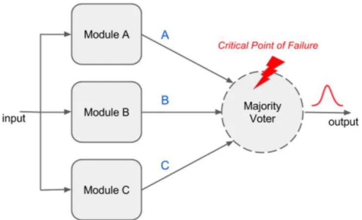
Fault tolerance is increasingly necessary for advanced technology circuits due to the high complexity and susceptibility to physical defects and environment disturbances as provoked by radiation interactions [1-4]. Safety- and mission-critical systems, such as satellites and aircraft flight control systems, are the primary applications using fault-tolerance techniques to improve reliability. A system is assumed to be fault-tolerant when its functionality is preserved even with the presence of faults. Commonly, redundancy is the core foundation of fault tolerance techniques proposed in the literature [3]. There is a variety of approaches, according to the redundant part added to the system, ranging from hardware and software to information and time redundancy [1]. Hardware redundancy, also known as spatial redundancy, is widely used in space applications due to its capability of performing fault detection and/or fault correction [2]. One of the most used technique is the so-called Triple-Modular Redundancy (TMR), in which the selected critical component or electronic circuit is triplicated and their outputs are connected to a majority voter (MJV) architecture, as shown in Fig. 1 [3]. Therefore, whenever two copies of the component are fault-free, the output of the majority voter will be also fault-free. However, if a fault occurs in the MJV, the technique fails to provide a correct function of the system.
The applicability of TMR schemes as a Radiation-Hardening-by-Design (RHBD) approach can extend from masking the effects of Single-Event Transients (SETs) in data paths or Single-Event Upsets (SEUs) in memory elements. However, the majority voter robustness against radiation effects is crucial for the fault detection and correction efficiency of TMR strategies. Few works in the literature have provided design studies on the radiation robustness of majority voters in terms of power, delay, area and SET cross-section [5-8]. The work developed in [5] provides heavy-ion experimental data and proposes a relative efficiency criterion for the majority voter selection according to the TMR strategy. Two FinFET-based majority voter circuits were evaluated under the atmospheric environment in [7]. In this case, the NAND- and NOR-based voter circuits have shown a similar soft-error rate (SER) due to
the symmetric sizing of the PFET and NFET devices provided by the strain engineering and width quantization at FinFET technology [7]. The work in [8] adopts a layout-level analysis through stick diagram to evaluate the diffusion area of majority voters and to calculate a fault masking ratio. Despite the layout-based approach, charge sharing between internal nodes and very importantly the intra-cell charge sharing effect in the multi-level circuit implementations are not considered, which can considerably increase the voter sensitivity or reduce it through pulse quenching effect [9]. Although the good fault coverage in TMR schemes, one of the main drawbacks of adopting redundancy-based hardening techniques is the considerably high increase in area and power consumption [1-3]. Thus, it is of utmost importance to adopt optimization strategies in the TMR block insertion to selectively address the most sensitive nodes in the target design and lower the impact on the area usage and power consumption.
In this work, a design exploration of majority voter architecture robust to SET effects is presented considering the SET cross-section dependence on the input signals. A Monte Carlo based prediction methodology is used along with the physical design information of each circuit to assess its sensitivity to high-energetic particle interactions. A deeper analysis of the input dependence of the circuit sensitivity is
Fig. 1. Diagram of the Triple Modular Redundancy (TMR) fault tolerance technique. Faults in the voter cannot be masked, thus it
constitutes the critical point of failure in the technique [7].
Cite this article as: Y. Q. Aguiar et al., "Design Exploration of Majority Voter Architectures based on the Signal Probability for TMR Strategy Optimization in Space Applications," in Microelectronics Reliability, vol. 114, November 2020, doi: 10.1016/j.microrel.2020.113877
provided. Therefore, the main contribution of this work lays on: the characterization of the input dependence of the SET cross-section in different majority voter architectures; and, the proposal of adopting signal probability analysis to provide an application-specific SET assessment of the designs and, consequently, to optimize the TMR insertion strategies in fault-tolerant systems for space applications.
This paper is organized as follows. The details on the circuit design and the SET assessment of the majority voter architectures are discussed in Section 2. Section 3 presents and discusses the results. Section 4 summarizes this work.
2. Circuit Design and Radiation Sensitivity Methodology The four majority voter architectures shown in Fig. 2 were designed based on a commercial 65nm bulk CMOS technology. In addition, they were designed to be compatible with the standard-cell library provided by the Product Design Kit (PDK). A fixed cell height is set to 13 tracks of the metal pitch, i.e. 2.6-µm high. To provide flexibility in the cell routing, intra-cell connections are primarily done using the metal 1 (M1), except for some cases in which metal 2 (M2) is used horizontally. The design of the two complex-gate majority voter followed the Euler’s path graph theorem to optimize their physical layout by
avoiding diffusion breaks and alleviating metal connectivity congestion [10]. For the cell-based implementations, the NAND2, NAND3, NOR2 and NOR3 were designed and characterized separately, as standard cells. Logical Effort (LE) sizing approach was applied to all circuits to provide a driving capability comparable of the minimum-sized inverter of the cell library [11]. The transistor sizing of the minimum-sized inverter has a PMOS/NMOS ratio of 190nm/135nm. Logical Effort approach is widely used in cell library design to achieve balanced delay performance. Accordingly, to provide means of comparison between MJV designs based on standard cells and complex CMOS implementations, only the LE sizing is adopted in this work.
The Euler’s path graph theorem is commonly used as a layout design optimization in which a transistor ordering is provided in such a way that diffusion breaks are avoided and metal connectivity is optimized. In Fig. 3, the Euler’s path graph theorem is applied to the CMOS2 voter. The pull-up and pull down transistor networks, i.e. PMOS and NMOS transistors, are translated into two graphs in which the vertices corresponds to the shared source/drain junctions of the circuit and the edges are the input signal of each transistor in the network. The Euler’s path, in summary, is the path that goes through all the vertices
Fig. 2. Circuit- and Layout-level implementations of the complex-gate and standard-cell-based majority voter architectures. For simplicity, only metal1 (blue), metal2 (orange), active diffusion (green) and poly (red) layers are shown.
in both graphs such that each edge is traversed only once. Not all transistor networks can provide a Euler’s path, however, it is also possible to obtain many path solutions for a given circuit. In the case of the CMOS2 voter represented in Fig. 3, one possible path is the ABCCB. In this work, the path ACCBAB and ABCCB are the Euler’s paths used to design the CMOS1 and CMOS2 layouts, respectively.
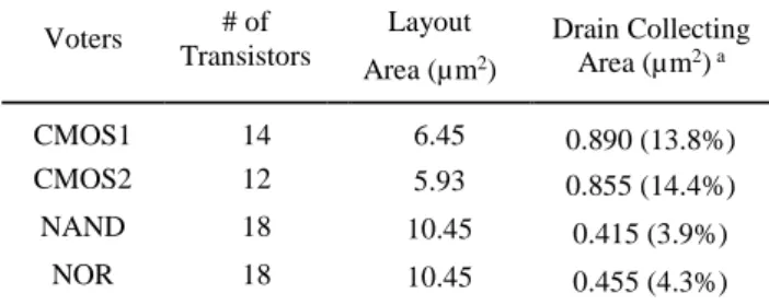
Table 1 presents the number of transistors and the layout and drain area information for each voter architecture. Due to the reduced number of transistor provided by the logic factoring, CMOS2 voter provides the smallest layout area. However, despite the larger number of transistors, the smallest drain collecting areas are observed for the cell-based implementations, with the smallest drain area for the NAND-based MJV. The two complex-logic implementations have about 2× the drain area of the cell-based designs. As logical effort is adopted to provide comparable driving strength, the 3-transistor stacks used in the two complex-logic design implementations increase the drain collecting area as the transistor width is upsized. Only about 4%
of the total layout of NAND and NOR voters represent the drain collecting area, while about 14% is expected for the CMOS1 and CMOS2 implementations. Thus, adopting complex-logic based MJV architecture provides a more compact and reduced layout
design. However, an increase in the drain collecting area is expected, affecting the overall SET susceptibility of the circuit by increasing the charge collection efficiency.
An SET predictive assessment was performed to calculate the cross-section and the in-orbit rate for Geostationary (GEO) and International Space Station (ISS) orbits. The layout-based SET assessment proposed in [12] was adopted. A Monte Carlo predictive tool, named MC-Oracle, is used to calculate the particle interactions within the collecting volumes extracted from the layout of the majority voters [13]. A SET database is generated containing the radiation-induced transient current for each sensitive node of the analyzed circuit [12]. Using a SET analyzer, a SPICE-based multi-node current injection is performed to calculate the cross-section and the SET pulse width distribution. An SET is occurred only if the resulting radiation-induced transient voltage exceeds at least half of the nominal supply voltage of the technology, i.e. peak voltage greater than VDD/2. Due to its layout-based approach and multi-node current injection methodology, charge sharing and pulse quenching effects (PQE) are considered in this analysis [14-16]. After the cross-section calculations, the in-orbit SET rate is estimated using the OMERE tool [17]. The Integral Rectangular Parallelepiped (IRPP) method is adopted as specified by the European Cooperation for Space Standardization (ECSS) [18]. The SET rate is calculated by the convolution of the cross-section curve with the particle flux obtained from the GEO and LEO (ISS) orbits. Following the European standard, a fixed shielding of 1 g/cm2 was used in the calculations, which the
international standard ISO 15390 model is used for the Galactic Cosmic Rays (GCR) [19] and the NASA AP8MIN trapped radiation model is used for the trapped proton flux under solar minimum (solar cycle 25) [20].
3. Results and Discussion
In this work, four majority voter architectures exploiting complex-gate and standard cells were designed based on a commercial 65nm bulk CMOS technology. The maximum, mean and standard deviation of the SET pulse width distribution is shown in Fig. 4 when considering a particle LET of 78.23 MeV.cm2/mg. The lowest pulse widths are observed for both
complex-gate MJV, the CMOS1 and CMOS2. This is attributed to the contribution of pulse quenching effect (PQE) inherent of inversion stages in combinational circuits [9]. As both CMOS1 and CMOS2 present an inverter gate in its output, the PQE is enhanced in these architecture and the overall SET distribution is shortened. Comparing the NAND and NOR based voters, the latter provides the wider distribution. This observation is agreement with the literature, as in [7] the FinFET-based NOR majority voter has also shown a wider SET distribution than the NAND implementation.
In Fig. 5, the SET cross-section for each circuit design is shown for two particle Linear Energy Transfer (LET) values, 78.23 and 9.94 MeV.cm2/mg. Although the two complex-gate
implementations, CMOS1 and CMOS2, present reduced layout,
Table 1
Number of transistors, layout and drain area of the CMOS1, CMOS2, NAND-based and NOR-based majority architectures
Voters # of Transistors Layout Area (µm2) Drain Collecting Area (µm2) a CMOS1 14 6.45 0.890 (13.8%) CMOS2 12 5.93 0.855 (14.4%) NAND 18 10.45 0.415 (3.9%) NOR 18 10.45 0.455 (4.3%)
a The percentage of layout design that corresponds to the
collecting drain area is also indicated
Fig. 3. Euler’s path graph theorem for the CMOS2 majority voter layout design.
they have showed the highest sensitivity for high and low LET. The reduced number of transistors of the CMOS2 implementation provided by logic factoring only induced a slight reduction of about 8% on the SET cross-section for high LET. On the other hand, an increase of about 26% is observed at low LET, when compared with the CMOS1 architecture. This can be attributed to the transistor restructuring and the consequent impact on the collecting area and the internal capacitance of the circuit.
Further, despite the larger design area, the lowest cross-sections were obtained for the NAND and NOR architectures. As observed in the previous section, by using smaller transistor in the cell-based designs a reduced drain collecting area can be achieved compared to the complex-gate implementations. However, these results provide the average cross-section obtained for logic input high and low. To better understand the design implications on the overall sensitivity of the circuit, the next subsection provides a discussion on the input dependence of the cross-section curve for each architecture.
3.1. Input Dependence of SET cross-section curves
The SET cross-section of the MJVs for the two possible input
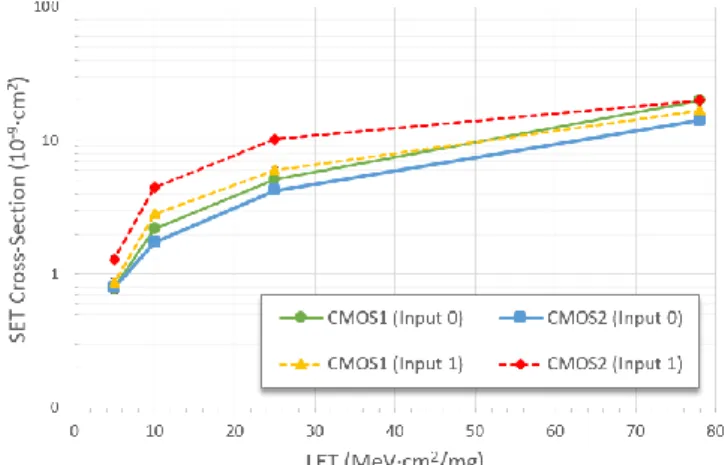
configuration in a fault-free TMR condition is studied: all inputs equal to 1; and, all inputs equal to 0. Considering the results for the complex-gate implementations in Fig. 6, the CMOS2 circuit has shown a higher input dependence than the CMOS1. This is attributed to the sizing and symmetry/asymmetry of the pull-up and pull-down transistor networks. The CMOS1 architecture allows a symmetric physical layout and consequently a balanced drain collecting area distribution. On the other hand, different sizing of each branch of the transistor networks in the CMOS2 architecture provides an asymmetric physical layout and an unbalanced distribution of the collecting areas, i.e. a considerably larger collecting area is observed for the PMOS devices than for the NMOS. Furthermore, both circuits have shown a higher cross-section for the input 1 configuration due to the larger PMOS devices and lower driving capability of NMOS devices.
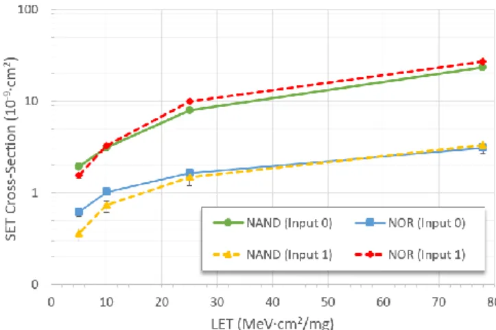
For the majority voters composed by basic logic standard-cells, a higher input dependence is observed as seen in Fig. 7. The nature of this variation is directly related to the logical masking effect capability of the 3-input NAND/NOR gate in the output of the circuit. For instance, when the TMR input configuration is at low logic level, i.e. all inputs equal to 0, for the NAND architecture, the output of the voter is sensitive to the SET occurrence in any of the 2-input NAND gate and the 3-input gate. On the other hand, for TMR input configuration at high logic level, i.e. all inputs equal to 1, the 3-input NAND gate is logically masking any of the SET in the 2-input NAND gates. The same phenomenon is observed for the NOR architecture, but the logical masking occurs when the TMR input configuration is set to low logic level. Thus, depending on the output signal of the triplicated blocks in the TMR, the NAND and NOR voters can provide a sensitive area only issued from the charge collection in its 3-input gate. Given the high input dependence of certain designs, the next subsection provides a signal probability analysis and discusses how it could be used to optimize the application of TMR schemes.
3.2. Signal Probability Analysis
Fig. 6. SET cross-section for the complex-gate architectures considering the two possible input configuration in a fault-free TMR scheme: all inputs in high logic level (Input 1); and, all inputs in low
logic level (Input 0). Fig. 5. SET cross-section estimation for CMOS1, CMOS2, NAND
and NOR majority voter architectures considering particle LET equals to 78.23 and 9.94 MeV.cm2/mg.
Fig. 4. Maximum, mean and standard deviation of the SET pulse width distribution for the CMOS1, CMOS2, NAND and NOR voters
The estimation of signal switching activity is widely used in circuit design to perform power analysis. However, it can also be used to perform reliability analysis as shown in [21]. For instance, consider the signal probability p as the probability of the signal to be in high logic level. And, as shown previously, the CMOS1 and CMOS2 architectures provide higher cross-sections for the input-1 scenario (Fig. 6). Therefore, the TMR insertion methodology should prioritize the insertion of these architectures in the sensitive nodes with the lowest signal probability. Considering the signal switching activity of the input signals, the gate cross-section σG can be calculated using
the Eq. 1 [12], where n corresponds to the number of input combinations, 𝜎𝑖 is the SET cross-section for input combination i, and 𝑝(𝑖) is the input combination signal probability. However, as in a fault-free TMR condition, the 3 input signals of the voter have the same signal probability p and only 2 input combinations (n = 2), then Eq. 1 can be reformulated as Eq. 2, where σMJV is
the majority-voter SET cross-section, pTMR is the signal
probability of the node in which the TMR will be inserted, 𝜎0
and 𝜎1 are the SET cross-section calculated for the two possible
input scenarios in a fault-free TMR condition, i.e. all inputs in low logic level (input-0 scenario) and all inputs in high logic level (input-1 scenario), respectively.
σG= ∑ 𝜎𝑖× 𝑝(𝑖) 𝑛
𝑖=0
(1)
σMJV= 𝑝TMR × (𝜎1− 𝜎0) + 𝜎0 (2)
Considering the Eq. 2, the SET cross-section curves were estimated for two signal probability and shown in Fig. 8 and Fig. 9, for p = 0.1 and p = 0.9, respectively. Notice that, for p = 0.1, in contrast with what we observed in Fig. 5, the NAND architecture provides the highest cross-section curve in Fig. 8. This is explained by the considerable high SET cross-section observed for the input-0 scenario (as shown in Fig. 7) and the low signal probability, p = 0.1. On the other hand, in Fig. 9, the NAND architecture provides the lowest cross-section, while the
NOR architecture provides the highest cross-section curves along with the CMOS1 and CMOS2 architectures. Thus, by considering the signal probability estimation to calculate the susceptibility of majority voter architectures, a more efficient and application-specific TMR insertion methodology can be obtained.
3.3. Impact on the in-orbit SET rate: GEO and LEO orbits
To verify the impact of a given radiation environment, Fig. 10 presents the SET rates estimated for three signal probabilities (p = 0.1, p = 0.5 and p = 0.9) and two different orbits (GEO and ISS/LEO). Two distinct trends can be observed: the increase of SET rate as the signal probability is increased; the decrease of SET rate as the signal probability is increased. Different from the CMOS1, CMOS2 and NOR architectures, the NAND voter is the only design that shows a decrease in the SET rate as the signal probability is increased. This is attributed to the lower SET cross-section for the input 1 configuration (Fig. 7) due to the logical masking effect. Additionally, the SET rate most sensitive to the input signal is observed for the NAND
Fig. 9. SET cross-section curves calculated for the majority voters considering a signal probability p of 0.9, i.e. higher probability of a
fault-free TMR condition in the input combination (1, 1, 1) Fig. 7. SET cross-section for the basic-logic gate architectures
considering the two possible input configuration in a fault-free TMR scheme: all inputs in high logic level (Input 1); and, all inputs
in low logic level (Input 0).
Fig. 8. SET cross-section curves calculated for the majority voters considering a signal probability p of 0.1, i.e. higher probability of a
architecture while the CMOS1 is the less sensitive, a variation of approximately 300% and 25 % from p = 0.1 to p = 0.9, respectively. In summary, considering the signal probability p = 0.1, p = 0.5 and p = 0.9, the best design for both orbits is the NOR, CMOS1 and NAND, respectively.
4. Conclusion
Redundancy-based hardening techniques are widely used to provide fault-tolerant systems. This work has evaluated the robustness of four majority voter architectures, which is the circuit that constitutes the critical point of failure in Triple-Modular Redundancy (TMR) methodologies. Also, a signal probability analysis is proposed as an optimization strategy for TMR block insertion algorithms. Despite the reduced layout design, complex-gate voter architectures have shown, on average, a higher SET cross-section than the implementations using basic logic standard-cell gates. As all architectures were designed to provide comparable driving strength, upsizing the stacked transistors in the complex-logic designs increases the charge collecting drain areas and, consequently, increases the SET cross-section of the circuit. Thus, aiming at a lower drawback in design area will compromise the reliability of the circuit. By evaluating the signal stimuli, a higher input dependence is observed for the basic-logic gate architectures due to the influence of logical masking effects. For instance, the 3-input gate in the output of the NAND and NOR architectures masks any SET in the 2-input gates when input scenario is high and low logic values, respectively. The SET rate for the CMOS1 architecture has shown to be the least dependent to the signal probability while the NAND voter showed the highest dependence. Furthermore, apart from the NAND voter, all the other design implementations have shown an increase in the SET rate as the signal probability is increased. Thus, to conclude, an SET assessment based on the input dependence analysis can provide further information to optimize selective TMR block insertion methodologies in the most critical nodes
of a circuit based on its signal probability. Acknowledgments
This work was realized within RADSAGA project. The RADSAGA Innovative Training Network project has received funding from the European Union’s Horizon 2020 research and innovation program under the Marie Skłodowska-Curie grant agreement number 721624.
References
[1] B. W. Johnson, “Fault-Tolerant Microprocessor-based Systems,” IEEE Micro 6 (1984): 6-21.
[2] M. Nicolaidis, “Design for soft error mitigation,” IEEE Trans. Device. Mater. Reliabil. 5.3 (2005): 405-418.
[3] F. L. Kastensmidt, L. Carro, and R. Reis. 2006. Fault-Tolerance Techniques for SRAM-Based FPGA (Frontiers in Electronic Testing). Springer New York, Inc., Secaucus, NJ, USA.
[4] R. C. Baumann, “Radiation-induced soft errors in advanced semiconductor technologies,” IEEE Trans. Device Mater.
Reliabil., vol. 5, no. 3, pp. 305–316, 2005.
[5] I. A. Danilov, M. S. Gorbunov, and A. A. Antonov, “SET Tolerance of 65nm CMOS Majority Voters: a comparative study,” IEEE Trans. Nucl. Sci. 61.4 (2014): 1597-1602.
[6] T. Ban, L. A. Naviner, “A Simple Fault-Tolerant Digital Voter Circuit in TMR Nanoarchitectures,” Procceedings of IEEE International NEWCAS Conference, pp. 269-272, 2010.
[7] Y. Q. Aguiar et al., “Evaluation of radiation-induced soft error in majority voters designed at 7nm FinFET technology,”
Microelectron. Reliab. 76-77 (2017): 660-664.
[8] I. F. V. Oliveira et al., “Single event transient sensitivity analysis of different 32 nm CMOS majority voters designs,”
Microelectron. Reliab. 100-101 (2019).
[9] J.R. Ahlbin, et al., The effect of layout topology on single-event transient pulse quenching in a 65 nm bulk CMOS process, IEEE Trans. Nucl. Sci. 57.6 (2010): 3380–3385.
[10] S. Rekhi, J. D. Trotter, and D. H. Linder, “Automatic layout synthesis of leaf cells”. Proceedings of the 32nd ACM/IEEE Conference on Design Automation, pp. 267–272, New York, NY, USA, 1995.
[11] I. E. Sutherland and R. F. Sproull, “Logical Effort: Designing for Speed on the Back of an Envelope,” IEEE Advanced Research in VLSI, pp. 1-16, 1991.
[12] Y. Q. Aguiar et al., “Mitigation and Predictive Assessment of SET Immunity of Digital Logic Circuits for Space Missions,”
Aerospace (2020): 1-12.
[13] F. Wrobel and F. Saigné, “MC-Oracle: a tool for predicting Soft Error Rate,” Comp. Phys. Comm. 182 (2011): 317-321.
[14] Y. Q. Aguiar et al., “Analysis of charge sharing effect in the SET sensitivity of bulk 45nm standard cell layouts under heavy ions,”
Microelectron. Reliab. 88-90 (2018): 920-924.
[15] Y. Q. Aguiar et al., “Impact of Complex-Logic Cell Layout on the Single-Event Transient Sensitivity,” IEEE Trans. on Nucl. Sci. 66 (2019): 1465 – 1472.
[16] Y. Q. Aguiar et al., “Radiation hardening efficiency of gate sizing and transistor stacking based on Standard Cells,” Microelectron.
Reliab. 100-101 (2019).
[17] The OMERE 5.3 Software by TRAD and CNES. Available online: http://www.trad.fr/en/space/omere-software (accessed on 10 October 2019)
[18] ECSS-E-HB-10-12A (2010) Space Engineering: Calculation of Fig. 10. In‐orbit SET rate calculated with OMERE [17] for the
Geostationary orbit (GEO), 35,784 km, and for the International Space Station (ISS) orbit, 400 km, 51.64°. Three signal probability is
radiation and its effects and margin policy handbook.
[19] ISO 15390, "Space environment (natural and artificial) - Galactic cosmic ray model", 2004.
[20] D. M. Sawyer and J. I. Vette, “AP-8 trapped proton environment for solar maximum and solar minimum,” NASA TM-X-72605, 1976.
[21] F. N. Najm, “Improved estimation of the switching activity for reliability prediction in VLSI circuits,” Proceedings of the IEEE Custom Integrated Conference, San Diego, CA, USA, 1994.