HAL Id: tel-03199411
https://tel.archives-ouvertes.fr/tel-03199411
Submitted on 15 Apr 2021
HAL is a multi-disciplinary open access archive for the deposit and dissemination of sci-entific research documents, whether they are
pub-L’archive ouverte pluridisciplinaire HAL, est destinée au dépôt et à la diffusion de documents scientifiques de niveau recherche, publiés ou non,
Prabir Mahato
To cite this version:
Prabir Mahato. Study and development of resistive memories for flexible electronic applications. Electronics. Université de Lyon, 2020. English. �NNT : 2020LYSEI134�. �tel-03199411�
i
-N°d’ordre NNT :
2020LYSEI134
THESE de DOCTORAT DE L’UNIVERSITE DE LYON
opérée au sein deINSA de Lyon
Ecole Doctorale N° ED160
Électronique, Électrotechnique et Automatique
Spécialité/ discipline de doctorat :
Électronique, micro et nano électronique, optique et laser Soutenue publiquement le 14/12/2020, par :
Prabir MAHATO
Study and development of resistive memories
for flexible electronic applications /Etude et
développement de mémoires résistives pour
l’électronique flexible
Devant le jury composé de :SCHINDLER Christina Munich University of Applied Sciences Rapporteur
PERRET Etienne ESISAR Rapporteur
CAIRONI Mario Istituto Italiano di Tecnologia Examinateur
BOCQUET Marc Aix- Marseille Université Examinateur
DELERUYELLE Damien INSA-Lyon Directeur de thèse
PRUVOST Sébastien PUYOO Etienne LE BERRE Martine INSA-Lyon INSA-Lyon INSA-Lyon Co-Directeur de thèse Co-encadrant Examinateur
SIGLE ECOLE DOCTORALE NOM ET COORDONNEES DU RESPONSABLE
CHIMIE CHIMIE DE LYON
http://www.edchimie-lyon.fr
Sec. : Renée EL MELHEM Bât. Blaise PASCAL, 3e étage
INSA : R. GOURDON
M. Stéphane DANIELE
Institut de recherches sur la catalyse et l’environnement de Lyon IRCELYON-UMR 5256
Équipe CDFA
2 Avenue Albert EINSTEIN 69 626 Villeurbanne CEDEX [email protected] E.E.A. ÉLECTRONIQUE, ÉLECTROTECHNIQUE, AUTOMATIQUE http://edeea.ec-lyon.fr Sec. : M.C. HAVGOUDOUKIAN [email protected] M. Gérard SCORLETTI
École Centrale de Lyon 36 Avenue Guy DE COLLONGUE 69 134 Écully
Tél : 04.72.18.60.97 Fax 04.78.43.37.17
E2M2 ÉVOLUTION, ÉCOSYSTÈME, MICROBIOLOGIE, MODÉLISATION
http://e2m2.universite-lyon.fr
Sec. : Sylvie ROBERJOT Bât. Atrium, UCB Lyon 1 Tél : 04.72.44.83.62 INSA : H. CHARLES
M. Philippe NORMAND
UMR 5557 Lab. d’Ecologie Microbienne Université Claude Bernard Lyon 1 Bâtiment Mendel 43, boulevard du 11 Novembre 1918 69 622 Villeurbanne CEDEX [email protected] EDISS INTERDISCIPLINAIRE SCIENCES-SANTÉ http://www.ediss-lyon.fr
Sec. : Sylvie ROBERJOT Bât. Atrium, UCB Lyon 1 Tél : 04.72.44.83.62 INSA : M. LAGARDE
Mme Sylvie RICARD-BLUM
Institut de Chimie et Biochimie Moléculaires et Supramoléculaires (ICBMS) - UMR 5246 CNRS - Université Lyon 1
Bâtiment Curien - 3ème étage Nord 43 Boulevard du 11 novembre 1918 69622 Villeurbanne Cedex Tel : +33(0)4 72 44 82 32 [email protected] INFOMATHS INFORMATIQUE ET MATHÉMATIQUES http://edinfomaths.universite-lyon.fr
Sec. : Renée EL MELHEM Bât. Blaise PASCAL, 3e étage Tél : 04.72.43.80.46
M. Hamamache KHEDDOUCI
Bât. Nautibus 43, Boulevard du 11 novembre 1918 69 622 Villeurbanne Cedex France Tel : 04.72.44.83.69
Matériaux MATÉRIAUX DE LYON
http://ed34.universite-lyon.fr
Sec. : Stéphanie CAUVIN Tél : 04.72.43.71.70 Bât. Direction [email protected] M. Jean-Yves BUFFIÈRE INSA de Lyon MATEIS - Bât. Saint-Exupéry 7 Avenue Jean CAPELLE 69 621 Villeurbanne CEDEX Tél : 04.72.43.71.70 Fax : 04.72.43.85.28
MEGA MÉCANIQUE, ÉNERGÉTIQUE,
GÉNIE CIVIL, ACOUSTIQUE
http://edmega.universite-lyon.fr
Sec. : Stéphanie CAUVIN Tél : 04.72.43.71.70 Bât. Direction [email protected] M. Jocelyn BONJOUR INSA de Lyon Laboratoire CETHIL Bâtiment-Sadi-Carnot 9, rue de la Physique 69 621 Villeurbanne CEDEX [email protected] ScSo ScSo* http://ed483.univ-lyon2.fr
Sec. : Véronique GUICHARD INSA : J.Y. TOUSSAINT Tél : 04.78.69.72.76 [email protected] M. Christian MONTES Université Lyon 2 86 Rue Pasteur 69 365 Lyon CEDEX 07 [email protected]
3
Abstract
The advent of flexible electronics has brought about rapid research towards sensors, bio implantable and wearable devices for assessment of diseases such as epilepsy, Parkinson’sand heart attacks. Memory devices are major component in any electronic circuits, only secondary to transistors; therefore many research efforts are devoted to the development of flexible memory devices. Conductive Bridge Random Access Memories (CBRAMs) based on creation/dissolution of a metallic filament within a solid electrolyte are of great research interest because of their simple Metal Insulator Metal architecture, low-voltage capabilities, and compatibility with flexible substrates.
In this work, instead of a conventional metallic oxide or a chalcogenide layer, a biocompatible polymer - Polyethylene Oxide (PEO) – is employed as the solid electrolyte layer using water as solvent. Memory devices, consisting in Ag/PEO/Pt tri -layer stacks, were fabricated on both silicon and flexible substrates using a heterogeneous process combining physical vapour deposition and spin coating. To aim this, a systematic study on the effect of solution concentration and deposition speed on the PEO thickness is presented. SEM/EDX and AFM measurements were then conducted on devoted “nano-gap” planar structures and have revealed the formation of metallic Ag precipitates together with morphological changes of the polymer layer after resistance switching. The performance of the resistive memory devices is then assessed on silicon and flexible substrates. In particular programming voltage statistics, OFF/ON resistance ratio, endurance cycles and retention tests are performed and the effect of current compliance is analysed. The conduction mechanism in the HRS/LRS is studied on the Ag/PEO/Pt and Pt/PEO/Pt reference devices. Finally, the electrical characterization of devices on flexible substrate is performed under mechanical stress, showing promising results. Polymer-based CBRAM devices are therefore suggested as potential candidates for sustainable development of flexible memory devices.
5
Acknowledgement
It has been a great pleasure and opportunity to carry out my PhD thesis work at the Institute Nanotechnology De Lyon – INL under the guidance of Prof. Damien Deleruyelle, who has guided me throughout the thesis. My thesis co-supervisor Dr. Etienne Puyoo has supported me throughout especially in the fabrication process and with valuable inputs in the characterization of the devices. My thesis co-supervisor from IMP- UMR 5523 CNRS, Dr. Sébastien Pruvost added his precious inputs on the polymer studies- development, processing, analysis and characterization that has been very enlightening.
I am grateful to Martine le-Berre for her guidance in analysing planar devices. I extend my gratitude to my lab director- Catherine Bru-Chevallier and team lead of Dispositifs electroniques Prof. Francis Calmon for providing such a conducive working environment. I express my thankfulness to our lab secretaries- Annie Suslec and Virginie Lagarde for easing me through the long institutional procedures. Sincere thanks to Liviu Militaru who guided me through the teaching procedures and schedules. I thank David Albertini for his AFM measurements and Solène Brottet for SEM measurements. I am grateful to Pierre Alcouffe for SEM EDX measurements on planar devices on the latest Quattro SEM. I thank all the members of Dispositifs electroniques group. I also thank the Director EEA Doctoral School Gerard Scorletti & Secretary Marie-Christine Havgoudoukian for their constant observation and guidance in my progress.
I am grateful to former Post doc/ PhD colleagues - Edgar Perez, Remi Rafael, Tulio Chaves, Getenet, Thais Vidal, Michele Calvo for easing me during this period. I thank Pierre Vincent (former PhD student) for supporting me in training for electrical characterization. I also thank PhD students- Sergio Casal-Gonzalez, Benoit Manchon for their support. I acknowledge the encouragement and support of my friends –Praveen, Abhinov, Carles, Florian Nivet, Elsa, Emeline. I am grateful to Houssém, Cécile for assisting me with the translation of the manuscript. I thank my athletic coaches- Bernard Pichon & Said Buguessa and my training friends who have given their effort and time to mould me into a better person.
Finally, I thank my parents, sister and grandparents for their unconditional love, support and sacrifices. At the end, I am grateful to everyone who has added growth to my personality through the vicissitudes of life.
7
Table of contents
GENERAL INTRODUCTION 11
CHAPTER 1- NON-VOLATILE MEMORIES FOR FLEXIBLE ELECTRONICS APPLICATIONS 13
1. OVERVIEW OF FLEXIBLE ELECTRONICS 13
1.1. Why do we need flexible electronics for? 13
1.2. Technological approaches and markets 17
2. OVERVIEW OF NON-VOLATILE MEMORIES TECHNOLOGIES 21
2.1. Volatile and Non-Volatile Memory in the semiconductor industry 21
2.2. Emerging Non-Volatile Memories 22
2.2.a. Charge-trap Memory 23
2.2.b. Ferroelectric RAM and emerging Ferroelectric devices 24
2.2.c. Phase-Change Memory (PCM) 25
2.2.d. Resistive RAM (RRAM) 26
2.2.e. Conductive Bridge-RAM (CBRAM) 28
3. FLEXIBLE NON-VOLATILE MEMORIES 30
3.1. Why non-volatile memories for flexible electronics? 30
3.2. Non-volatile memories for flexible electronics 31
3.3. Flexible CBRAM devices 33
3.3.a. CBRAMs based on a chalcogenide layer 33
3.3.b. CBRAMs based on a polymer layer 35
3.3.c. Towards flexible biopolymer-based CBRAMs 37
4. CHAPTER CONCLUSION, RESEARCH WORK OBJECTIVES AND MANUSCRIPT ORGANIZATION 39
5. REFERENCES 41
CHAPTER 2 - FABRICATION PROCEDURE OF POLYMER BASED CBRAMS 47
1. SOLID POLYMER ELECTROLYTE LAYER PREPARATION & ANALYSIS 47
1.1. Polyethylene oxide (PEO) properties 47
1.2. Polyethylene oxide (PEO) film preparation 48
1.2.a. Un-doped PEO solution 48
1.2.b.Doped PEO solutions 49
1.3. Analysis of PEO layer by Differential Scanning Calorimetry (DSC) measurements 50
1.3.a. Experimental setup 51
2. THICKNESS CONTROL OF PEO LAYER & ITS MORPHOLOGICAL OBSERVATION 54
2.1. Influence of spin parameters coating on PEO thickness 54
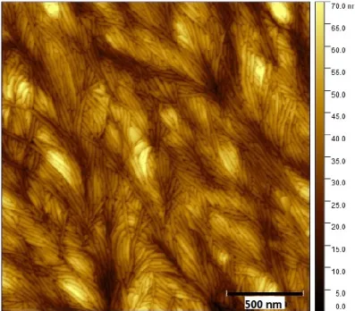
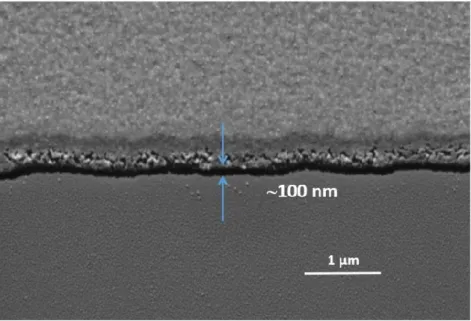
2.2. AFM and SEM images 56
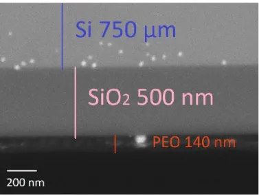
3. FABRICATION OF CBRAM DEVICES 59
3.1. Polymer based CBRAM devices on Silicon substrates 59
3.1.a. Vertical devices 59
3.1.b. Planar devices 61
3.2. Polymer based CBRAM devices on flexible substrates 65
4. CONCLUSION TO THE CHAPTER 67
5. REFERENCES 68
APPENDIX A : DSC MEASUREMENTS 71
APPENDIX B : XRD MEASUREMENTS 73
APPENDIX C : FTIR MEASUREMENTS 77
APPENDIX D : SHADOW MASKS 81
CHAPTER 3 – ELECTRICAL CHARACTERIZATION AND ANALYSIS OF VERTICAL CBRAM DEVICES 83
1.EVIDENCE OF CBRAM-TYPE SWITCHING 83
1.1. Experimental setup 83
1.2. Evidencing the role of electrodes and voltage polarity 84
1.3. Effect of PEO thickness 86
2. ELECTRICAL PERFORMANCE OF THE DEVICES 87
2.1. Evidence of the effect of compliance current 88
2.2. Cycling at various current compliance 88
2.2.a. Impact of compliance current on the programming voltages 89
2.2.b. Impact of compliance current on resistance distribution 90
2.2.c.Volatile vs Non-Volatile switching 92
2.2.d.Volatile CBRAMs as selectors ? 93
2.2.e. Retention time 95
2.3. Conclusion to the section 96
3. ANALYSIS OF CONDUCTION MECHANISMS IN PT/PEO/PT AND AG/PEO/PT DEVICES 97
3.1. Analysis of Pt/PEO/Pt devices 97
3.1.a.Schottky emission 99
3.1.b.Poole Frenkel emission 100
9
3.2. Analysis on Ag/PEO/Pt devices 102
3.2.a. Low Resistance States (LRS) 104
3.2.b. High Resistance State (HRS) 105
3.3. Conclusion 106
4.CONCLUSION TO THE CHAPTER 108
5.REFERENCES 110
APPENDIX E: REVIEW OF CONDUCTION MECHANISMS 113
APPENDIX F: BOX PLOTS 119
APPENDIX G: JUNCTION BARRIER HEIGHT CALCULATION 121
CHAPTER 4 - STUDY OF PLANAR CBRAM DEVICES: ELECTRICAL, PHYSICAL AND CHEMICAL ANALYSES 123
1. ELECTRICAL CHARACTERIZATION 123
1.1. SET/RESET voltage statistics & memory window 123
1.2. Endurance cycles 124
1.3. Retention time 126
1.5. Electrical Characterization of doped devices 128
2.MORPHOLOGICAL OBSERVATION ON PLANAR DEVICES 129
2.1. Micrographs of planar un-doped devices 130
2.2. Micrographs of planar doped devices 132
2.3. Atomic Force Microscopy (AFM) images on planar devices 133
3.SEM/EDX ANALYSIS 136
3.1. Analysis of un-doped planar devices 136
3.1.a.Observation on a pristine device 137
3.1.b.Observation of cycled devices 139
3.2. Analysis of doped planar devices 142
3.2.a.Observation on a pristine device 142
3.2.b.Observation on cycled doped device 142
4. CONCLUSION TO THE CHAPTER 145
5. REFERENCES 146
CHAPTER 5 – POLYMER-BASED CBRAMS ON FLEXIBLE SUBSTRATES 149
1.STUDIED DEVICES AND EXPERIMENTAL SETUP 149
1.1. Studied devices 149
1.2. Electrical and mechanical characterization setup 149
2.1. SET/RESET voltage statistics 150
2.2. Endurance measurement and programming window 152
2.3. Retention time 154
3.ELECTRICAL CHARACTERIZATION UNDER MECHANICAL STRESS 154
3.1. Bending cycles 154
3.2. Cell programming under mechanical bending 157
4.EFFECT OF AREA AND CURRENT COMPLIANCE: COMPARISON BETWEEN FLEXIBLE AND SILICON SUBSTRATES 159
4.1. Impact on LRS and HRS 160
4.2. Impact on programming voltages 161
5.STUDY OF CONDUCTION MECHANISM IN LRS AND HRS 163
5.1. High Resistance States (HRS) 164
5.2. Low Resistance States (LRS) 165
6.CONCLUSION TO THE CHAPTER 168
7.REFERENCES 169
GENERAL CONCLUSIONS AND PERSPECTIVES 171
11
General Introduction
Internet of things (IoTs) with its applications in the field of health, production, security and transport is changing the dynamics of security systems, usage and control around the world. In this respect flexible electronics is expected to play a major role as it possess the advantages of using large areas and curved substrates, downscaling the resolution of fabrication of the devices, easing processability and lowering production costs. Gradually, with technological advancements many commercial products such as sensors, light emitting diodes and wearables are being part of our daily routine. Besides logic transistors, memory devices are important component of any electronic circuit. The fact that volatile memory devices categorized as SRAMs or DRAMs lose data when switching off power supplies brings non-volatile memory devices into the spotlight. Among them, Flash memories have a significant share in the market due to their high density, stability in performance and low cost. However, the disadvantages of high write voltages (>10V), low operation speed (in milli seconds), limited endurance cycles 103-105 and large leakage
currents make us look beyond them.
Among the emerging non-volatile memories, Conductive Bridge Random Access Memory devices (CBRAMs) are gaining attention due to their simple architecture – Metal-Insulator-Metal (MIM), ease of process ability and scalability. Research on CBRAMs have shown exceptional properties of fast response time, possibility of multilevel data storage by modulating the compliance current, high density, low power consumption and high performance.
In this research work, we develop and study the performance of CBRAMs based on solid polymer electrolyte layer, Polyethylene oxide (PEO). After the validation of the fabrication process, the workability of the devices are reported through current-voltage characteristics in order to evaluate their retention time, endurance cycles and so on. As these devices are based on switching mechanism between ON and OFF states through a conductive filament. Planar devices with nano-gaps are fabricated to observe the filament growth. Through optical microscope, AFM, SEM and EDX measurements such
morphological changes are observed. Further, conduction mechanism studies are carried out to understand the factors influencing the charge transport in such thin films.
Finally moving towards our goal, as the use of polymer layer facilitates deposition on flexible substrates. Hence, the devices are fabricated on kapton- 125 µm. Fatigue tests are performed on the devices to study their resilience to stress. Hence, this work aims at sustainable development of CBRAMs for flexible electronic application.
- 13 -
Chapter 1- Non-Volatile memories for flexible
electronics applications
This chapter introduces flexible electronics, which is the main context of this work. After presenting the main advantages of flexible electronics to support the deployment of the so-called “Internet of Things” infrastructure, we will expose the different technological approaches supporting its development together with current market and opportunities for growth.
We will then focus on non-volatile memories, showing how these devices can contribute to the development of smart autonomous objects. Among the large family of Non-volatile memories, emerging memories based on resistance switching are considered today as potential candidates to replace traditional Flash memories based on charge-storage. Among them, Resistive Random Access Memories (RRAM) and Conductive-Bridge Random Access Memories (CBRAM) are very promising due to their overall performances and ease of fabrication. In particular, it is shown that such kind of memories can be engineered using polymer films, which make them very appealing for flexible electronics applications.
Finally, we conclude on this chapter through a presentation of the main objectives of the PhD work.
1. Overview of flexible electronics
1.1. Why do we need flexible electronics for?
Since the 70s’, the global electronics market is taking advantage from the constant progress achieved in the semiconductor industry, ruled itself by the so-called “Moore’s Law” [1]. While moving from one technology node to the next one, downscaling the integrated devices can be leveraged through a decrease of fabrication costs (i.e. reduction of the circuit area) while keeping the same amount of functionalities, by increasing the computing energy efficiency while keeping the fabrication costs, or by enabling new functionalities through the integration of novel devices [2]. This virtuous dynamic
combining lower production costs, increased integration density, performances and functionalities has led to a growth of the electronics market through successive “waves” from analogue (1970-1980), digital (to from 1990), internet (end of the 90s) and mobile electronics (2000s).
Today, the electronic market is riding on the so-called “Internet of Things” (IoT) wave. In its broad sense, IoT designates software and hardware infrastructure making possible to connect, through the Internet, humans to any "object" lying in their physical environment. Today, it is estimated that more than 20 billions of object are connected through the IoT infrastructure (more than twice the worldwide population) and that this number is about to triple by 2025 [3].
As shown in Figure 1. 1, it is forecasted that IoT and automotive applications will feature the highest growth-rate until 2021 [4].
Figure 1. 1 Forecast of market share and growth rates for different sectors covered by integrated circuits between 2016 and 2021. Source : IC Insights [4]
CHAPTER 1
15 Figure 1. 2 illustrates the numerous applications that can be covered by IoT; it is shown that all current major social challenges such as health, energy, food or transport can take advantage of IoT. In addition, it is apparent that the deployment of IoT sensor nodes rely on elementary electronic devices functionalities such as data acquisition (sensor), processing (logic), storing (memory), transmission (RFID) associated with power solutions [5]. Even though such elementary functionalities are already available in CMOS (Complementary Metal Oxide Semiconductor) technologies, silicon-technology suffers from severe limitations regarding integration within a wide variety of “objects” of our daily life having arbitrary areas and shapes [6].
Figure 1. 2 Illustration of the IoT infrastructure linking applications and the elementary electronic devices required for their deployment. Adapted from [5]
Figure 1. 3 Teardown of an Apple Watch © Serie 5 showing the complex packaging of Printed Circuit Boards, electronic modules and battery interconnected through flexible connectors. Source: iFixit.com
Indeed, as illustrated in Figure 1. 3, most of the modern electronic systems still rely on rigid substrates (i.e. PCB - Printed Circuit Board) holding Integrated Circuits (ICs). This approach, suffers from limitations regarding its integration into objects featuring large areas and arbitrary form factors. Even though technological options exists to thin silicon IC and transfer them onto flexible substrates [7], CMOS technologies are not naturally adapted to be integrated onto non-planar surfaces. In addition, their fabrication cost still remain prohibitive regarding the development of large area electronics (>10cm2) [8].
Given these limitations, flexible electronics can be a key-enabling technology to extend the integration of electronic functions into a wide range of objects for IoT applications together with lowering their fabrication costs. Indeed, flexible electronics can employ various affordable deposition techniques, such as inkjet printing or screen printing and does not necessarily require heavy and costly techniques such as photolithography to achieve electronic functions. In addition the use of flexible substrates such as polymer films, which are commercially available in the form of large rolls, techniques like « roll-to-roll » processing can be leveraged to elaborate electronic circuits over large areas [9]. Besides plastics, many other kind of substrates such as textiles[10] or even human skin [11] where demonstrated to be capable to host electronic functions strengthening therefore the interest for flexible electronics market for IoT.
CHAPTER 1
17 1.2. Technological approaches and markets
According to the FLextech Alliance1 (international consortium of research and
industrial laboratories established since 1993) flexible electronics covers a wide variety of fabrication techniques schematized in Figure 1. 4 :
• Printed Electronics [Figure 1. 4(a)] functional electronics fabricated by laying conductive lines using one of several printing methods, including: screen, ink-jet, gravure, flexography and others. Often confused with printed circuit boards, which also use printing methods to connect discrete active and passive components. Plastic Electronics [Figure 1. 4(b)] refers to the fabrication of circuit or electronic functions onto plastic (i.e. polymer) substrates using processes not restricted to printed electronics. Vacuum deposition methods or photolithography can be then deployed on plastic substrates.
• Flexible Electronics [Figure 1. 4(c)] refers to a class of electronic devices built on conformable or stretchable substrates, usually plastic, but also metal foil, paper or glass. • Organic Electronics [Figure 1. 4(d)] concerns the fabrication of electronic functions or
devices (i.e. transistors, sensors, memory,…) employing organic compound or polymer filmsi.
• Flexible Hybrid Electronics (FHE) [Figure 1. 4(e)] can be viewed as a synthesis of the aforementioned technologies, which can also combine silicon (CMOS) electronics. In it broad sense, FHE can be viewed as an heterogeneous integration technique taking advantage of flexible electronics for processing functionalities onto large area or arbitrary shaped substrates without sacrificing performances through the integration of silicon ICs.
Figure 1. 4 Illustration of the various technological approaches embraced by flexible electronics in its broad sense.
(a) Printed Electronics: Example of a pressure sensor fabricated printed on a flexible substrate [12]. (b)
Plastic Electronics : Non-volatile Memories fabricated on kapton substrates where electrodes where
achieved by photolithography [13]. (c) Flexible Electronics : TFT (Thin Film Transistors) fabricated on a flexible steel sheet [14]. (d) Organic Electronics : PVK (Poly-Vinyl Carbazole) matrix deposited on a flexible substrate containing CdSe/ZnS core-shell nanoparticles for non-volatile memories [15]. (e) The combination of these various techniques can be associated to the integration of silicon ICs to achieve a
Flexible Hybrid Electronics: here an electronically designed Bluetooth enabled flexible “Smart Inhaler” [16].
Figure 1. 5 shows the main market sectors of printed, flexible and organic electronics as reported by IDTechEx2 for year 2019. This $30 billion global market is forecasted to grow
to $41.2 billion in 2020 and up to $74 billion in 20302. (e)
Flexible Hybrid electronics
(b) Printed electronics (a) Silicon Electronics Plastic Electronics (b) Flexible Electronics (c) (d) Organic Electronics
CHAPTER 1
19 (a)
(b)
Figure 1. 5(a) Current markets of printed, flexible and organic electronics as by IDttechEx Research group. (b) Forecast by Inkwood Research of the global flexible electronics market including applications and components from 2017-2026.
Sources : IDTechEx [17]
Regarding the main functionalities embraced by this market, it can be seen that its major components are a) flexible displays - such as OLEDs - Organic Light Emitting Devices devoted to the TV, mobile phone or tablets. (b) conductive inks - used in a wide range of applications such as In Mold Electronics [18][19] ; e-textiles [9], RFID [5],…) and (c) printed and flexible sensors [20]. As flexible electronics are gaining maturity, new market trends such as wearable electronics [Figure 1. 6] or smart-packaging applications [Figure 1. 7] are soon expected to be strong market sectors of flexible electronics.
Figure 1. 6 Shows an electronic skin patch - an integration of flexible and printed electronics with conventional electronics to create a wearable patch. Holst Centre predicts healthcare trends and opportunities growing doubling from 2019 to 20243.
CHAPTER 1
21
2. Overview of Non-volatile Memories technologies
This section provides an overview on the main technologies of non-volatile memories. Starting from the mainstream Flash technology and their integration limits, the emerging non-volatile memories are introduced together with their physical principle. Although most of the technologies discussed here are based on semiconductor devices, this section is intended to serve as introduction of the flexible non-volatile memory technologies presented in the next section.
2.1. Volatile and Non-Volatile Memory in the semiconductor industry
Memory technologies can be broadly divided into two categories: Volatile and Non-Volatile memory (i.e. NVM). In volatile memory, data is instantaneously lost as soon as the power is shut down. In return, these devices are well suited for quick computation and programming given their low access time (i.e. < 10 ns). The Static (SRAMs) and Dynamic (DRAMs) are the main representatives of volatile memory. Both are respectively used as cache and main memory in computing system, the SRAM being co-integrated with the CPU while DRAM is accessed externally from dedicated modules[21].
Figure 1. 8 (a) Schematic view of a Flash memory cell and (b) its ID (VG) characteristics. The
programming principle relies on the injection of charge to/from the floating gate from/to the silicon channel by tunneling effect. From [22]
Currently, Flash memory is the mainstream technology in the field on non-volatile memory. The reason for such an industrial success is the continuous downscaling of the Flash memory cell since its introduction on the market by Toshiba in the late 1980s [23].
The main principle of Flash memory is depicted in Figure 1. 8 : the cell consist of a transistor featuring an additional floating gate insulated from the silicon channel by a thin (~5-7 nm) tunnel oxide. Memory effect is achieved by charge injection from the silicon channel to the floating-gate resulting in a threshold voltage shift of the Flash memory transistor [Figure 1. 8].
There are two main kinds of Flash memories, depending on the cell arrangement in the memory array: NAND and NOR types. The NOR ones are used as embedded memory in microcontrollers [21], while the NAND ones, due to a denser implementation are primarily found in standalone NVM modules for USB flash drives, Solid State Drives (SSD) and mobile devices (e.g.: smartphones and tablets). Due to its larger integration density and given the high demand for NAND Flash memory for mobile applications and SSD applications over the last decade, NAND Flash has been aggressively downscaled down to the 10 nm node as early as in 2011[24].
Although Flash memory is a very attractive and mature technology, it possesses intrinsic limitations such as single electron effects [25], parasitic electrostatic coupling between
adjacent cells [26] or Stress Induced Leakage Current (SILC) which makes the tunnel oxide
hardly scalable beyond 5 nm [27] which in turn results in a limited voltage scalability for both standalone and embedded applications. For these reasons Flash scaling is highly compromised beyond the 28 nm node for NOR applications and 10 nm for standalone NAND [28].
2.2. Emerging Non-Volatile Memories
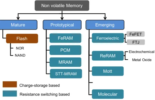
The scaling limits of Flash memory has stimulated intense R&D efforts in order to design emerging non-volatile memories over the last decades [29][26][27]. Given the fact that no universal memory exists, that would combine integration density and non-volatility of Flash together with programming speed of SRAM, a wide variety of emerging memories are still under development as schematized in Figure 1. 9 [31]. It can be seen that most of the alternative technologies for Flash memory exploit resistance switching as main physical principle instead of charge-storage.
CHAPTER 1
23 Figure 1. 9 Overview of emerging non-volatile memories sorted along their technological maturity.
Source : ITRS 2.0 – Emerging Research Devices [31] (adapted)
Given most of the flexible memories take their inspiration from the developments undertaken on semiconductor technologies [32], in the following we will briefly describe the main concepts behind the main alternative technologies to Flash memory explored on flexible substrates.
2.2.a. Charge-trap Memory
During each erase/write cycle, the electrical stress degrades the tunnel oxide, generating traps within the bandgap of the tunnel oxide. This phenomenon is known as SILC (Stress Induced Leakage Current) and results in a progressive degradation of the Flash memory retention capabilities over cycling [27]. In order to ensure immunity to SILC, the tunnel oxide of Flash memory cannot be downscaled beyond 5-7 nm in order to ensure the 10 years data-retention criterion, resulting in a limited programming voltages scalability. In order to cope with SILC, the replacement of the continuous polysilicon floating gate by a
discrete charge-trap layer (such as a nitride Si3N4 layer) was suggested in order to increase NOR
FeRAM PCM MRAM STT-MRAM Non volatile Memory
NAND FeFET FTJ Prototypical Mature Flash Electrochemical Metal Oxide Emerging Ferroelectric ReRAM Mott Macromolecular Molecular Charge-storage based Resistance switching based
localization of the stored charge and avoid a complete discharge of the memory cell as defects are generated within the tunnel oxide [Figure 1. 10].
Figure 1. 10 Schematic view of a conventional floating-gate based Flash memory cell: SILC induces early charge leakage through traps generated in the tunnel oxide. (b) Charge-trap memory concept: the polysilicon floating gate is replaced by a continuous charge-trapping layer (i.e. Silicon Nitride) in order to prevent charge leakage due to SILC. From [29]
This type of memory cell is commonly referred as SONOS (Silicon Oxide Nitride Silicon) in relation with the composition of the memory gate stack [33].
2.2.b. Ferroelectric RAM and emerging Ferroelectric devices
Ferroelectric memories rely on the same physical switching mechanism; switching due to the reversal of spontaneous electric polarization of a thin ferroelectric film under an electric field. Given this principle, a FeRAM memory cell consists in a 1 transistor-1 capacitor (1T1C) where the ferroelectric film is sandwiched within the capacitor. Reading is achieved through a current measurement achieved during the application of a voltage pulse across the ferroelectric capacitor in order to detect a polarization reversal current (reading can therefore be destructive).
CHAPTER 1
25
(a) (b)
Figure 1. 11. Illustration of ferroelectricity-based non-volatile memories. (a) 1T1C FeRAM and 1TFeFET and,, (b) Ferroelectric Tunnel Junction (FTJ). Adapted from [34]
The first commercial prototypes of FeRAM were demonstrated in 1988 using the most common ferroelectric such as PbZrTi (PZT) and SrBi2Ta2O9 (SBT) [35][36].
However, due to low coercive fields and high annealing temperatures, these materials could not be integrated beyond the 180 nm node [37]. The recent discovery of ferroelectricity in doped HfO2 has renewed the interest for ferroelectric memory since 2011 [38], [39]. Given
its excellent compatibility witch CMOS technology and it low annealing temperature (<450°C) ferroelectric HfO2 can be integrated within the gate stack of transistors to achieve
1T Ferroelectric FET (1T-FeFET) memory cells [Figure 1. 11]. Another option to exploit ferroelectricity for non-volatile memory is to exploit the Tunnel Electro Resistance (TER) contrast within a Ferroelectric Tunnel Junction (FTJ) as depicted in [Figure 1. 11]. In this case, the barrier height modulation due to polarization reversal induces an asymmetric band bending resulting in a distinct resistance states [40].
2.2.c. Phase-Change Memory (PCM)
PCM devices exploits the large electrical resistivity contrast between the amorphous and the crystalline states of chalcogenide glasses (the most commonly used alloy is Ge2Sb2Te5, namely GST) to store binary states [41]. As depicted in Figure 1. 12 the device
consists of a top electrode, the chalcogenide phase change layer, and a bottom electrode. The bottom electrode contact is achieved through a confined “heater” in order to promote confinement of the current lines and therefore improved thermal heating in the vicinity of the chalcogenide/heater interface.
(a) (b)
Figure 1. 12 Schematic cross-section of conventional PCM cell: resistance switching is due the localized reversible phase transition of a phase-change material in the vicinity of a confined “heater” contact. (b) Illustration of the temperature profile during the different operating sequences of the PCM cell. From [41].
The PCM operation is depicted in Figure 1. 11; during set the chalcogenide alloy is melted above its crystallization temperature through the application of a voltage pulse resulting in the formation of a low resistive crystalline phase. The reverse reset operation (i.e. crystalline to amorphous transition) is achieved through the application of a short electric pulse with a larger temperature during which the chalcogenide alloy is momentarily heated above its melting temperature and then quickly quenched into an amorphous phase with high resistivity. Finally, the resistance state of the cell is read through a voltage pulse at low voltage.
2.2.d. Resistive RAM (RRAM)
Figure 1. 13 depicts the architecture of a RRAM cell. The device consists in a simple Metal-Insulator-Metal architecture where a resistive switching layer is sandwiched between two metallic electrodes. Resistance switching is mainly observed within metallic oxides (such as TiO2, HfO2, Ta2O5) and is controlled by the creation/migration of oxygen vacancies due
CHAPTER 1
27
Change Memory or OxRAM (Oxide RAM) memories [42][43]. As the electric field
approaches the breakdown field, oxygen ions/oxygen vacancy pairs are created and migrate across the metallic oxide. Since oxygen vacancies act as discrete electronic states within the bandgap of the oxide, a localized conduction path is initiated inducing then Joule heating. Finally the interplay between oxygen vacancy generation and Joule heating result in the creation of a conductive filament bridging top and bottom electrodes [44].
The device is then set in a so-called Low Resistance State (LRS). The opposite reset operation is also achieved through the application of a voltage sweep (or voltage pulse) having the same or an opposite polarity leading to unipolar or bipolar operations [Figure 1. 13]. In this case it is the combination of Joule heating and oxygen vacancy recombination which leads to a partial breakdown of the conductive filament [Figure 1. 13] and restoring a High Resistance State (HRS).
It has to be noted that the first resistance switching, operated on a pristine state, is generally achieved at a higher voltage than subsequent set operations. This stage corresponds to the forming or electro-forming operation [44], [45]. During the set operation the current flow through the device has to be controlled in order to avoid an irreversible dielectric breakdown of the oxide. This current limitation can be achieved through the use of the current compliance (Icomp) of the parameter analyzer or by putting a current limiting
device in series with the memory cell such as a resistor or a transistor [46].
Top Electrode
Bottom Electrode
Low Resistance State (LRS)
High Resistance State (HRS) x x x x Top Electrode Bottom Electrode Oxygen ion (O-,O2-) Oxygen vacancy (VO+,VO2+) Metallic
oxide Metallicoxide
Conductive filament (a) (b) VTE VBE Unipolaire Bipolaire Icomp Icomp (a) (b) (c)
Unipolar switching Bipolar switching
(c) (d)
Figure 1. 13 Schematic view of a RRAM cell (a) in its Low Resistance State (HRS) and (b) High Resistance State (HRS). Resistance switching is due to the reversible creation/dissolution of an oxygen-vacancy rich conductive filament within a metallic oxide. Resistance switching can be either (c) unipolar or (d) bipolar.
2.2.e. Conductive Bridge-RAM (CBRAM)
Conductive-Bridge RAM (CBRAM) also referred as Electro Chemical Memory (ECM) [47] or Programmable Metallization Cell (PMC) [48] can be viewed as a close technology from RRAM in the sense that they also rely on the reversible creation/dissolution of a conductive filament within an insulating material. The working principle of CBRAM devices is illustrated in Figure 1. 14.
The device structure consists in an insulating Solid Electrolyte Layer (acting as a ion-conductor layer) sandwiched between an oxidizable Active Electrode (i.e. Ag or Cu) and an (electrochemically) inert Counter-Electrode (e.g.: Pt) [47].
Figure 1. 14 Typical current-voltage characteristic of a Conductive-Bridge RAM (CBRAM). Figures (A)-(E) in inset describe the elementary processes responsible for resistance switching: (A): virgin cell, (B): active electrode oxidization and cation migration. (C): Electrodeposition of metallic cations at the counter-electrode resulting in (D) the formation a metallic-rich conductive filament. (E) Oxidization of the conductive filament resulting in the opening of a gap. From [47].
CHAPTER 1
29 Resistance switching is induced by successive elementary processes denoted from (A) to (E) in Figure 1. 14 depending on the polarity of the applied voltage with respect to the active electrode (i.e. Ag or Cu).
Starting from a pristine cell [Figure 1. 14], the application of a positive voltage induces
anodic dissolution of the active electrode given the following reaction [Figure 1. 14]:
𝐴𝑔 → A+g + e−
Due to the electric field within the solid electrolyte layer, cations migrate toward the counter-electrode (i.e. cathode) where they can be electrochemically reduced according to:
𝐴𝑔++ 𝑒− → 𝐴 𝑔
This process initiates the growth of a conductive filament extending from the inert toward the active electrode [Figure 1. 14]. Due to the increased electric field at the apex of the conductive filament and the continuous dissolution of metallic cations within the solid electrolyte, the filament grows until it reaches the active electrode, resulting in the set operation [Figure 1. 14]. The cell remains in its Low Resistance State until a sufficiently negative bias is applied to electrochemically dissolve the conductive filament during the
reset operation [Figure 1. 14.E]. As for RRAM technology, a strong interplay between
oxidization/reduction rates and joule heating is also expected during set and reset operations [49].
If active electrodes generally consist of copper or silver, a wide variety of materials has been demonstrated for both the solid electrolyte layer and the counter-electrode [50][51][52]. The different classes of materials use for the solid electrolyte layer include
mixed (ion-electron) conductors based on chalcogenide alloys such as (non exhaustively)
Cu2S or Ag2S [53], Ag or Cu doped GeSex [54][55], Cu-GeTe [56], Ag-Ge2Sb2Te5 [54][55],
insulators and metallic oxides (e.g. SiO2, Al2O3, GdOx)[59][60][61] and
polymer/biopolymer materials such as Polyethylene Oxide [62]–[64], chitosan[65] or aloe
vera [66]. Note that this latter class of material is of particular interest for flexible electronics, given their inherent mechanical flexibility, processability over large areas and affordability.
3. Flexible Non-Volatile Memories
3.1. Why non-volatile memories for flexible electronics?
Flash Memory is the major technology in the field of non-volatile memory, due to a market highly stimulated by mobile electronics [22]. Today, integration densities as high as 1TB on a single die are commercially available3. In this context, it would seem illusory to
attempt to compete with Flash technology with flexible memories for mass storage applications. However, as shown in Table 1. 1, there is a need for low memory densities from few bits to kbits for applications such as e-tickets, RFID tags [67] or for storing as small volume of data near a sensor for wearable devices [68][69]. In addition, some of these applications only require One Type Programmable (OTP) or WORM4 type of non-volatile
memories. In this context, flexible non-volatile memories can be very advantageous as they
could be directly processed onto the flexible substrate without requiring additional
integration steps such as soldering a Non-volatile memory module.
Parameter
Desired
Retention Month/Year
Write Time µs to ms
Read Time µs to ms
Programming Voltage <24V
Type of Memory Strongly dependent on application
Single Use (WORM4)
Rewritable
Memory Array size Strongly dependent on application
RFID : 8 to 128 bits
Smart packaging, toys, smart-cards, badges, e-tickets, wearables, sensor node :
1-64kbits
Area Less critical
~mm2 or more
Endurance Strongly dependent on application
103 to 106 cycles
Operating temperature Archival : -40°C to +85°C
Operating: -20°C to +50°C
CHAPTER 1
31 Figure 1. 15 gives an illustration of the kind of new opportunities that can be brought by flexible non-volatile memory devices.
Figure 1. 15 Picture of a wearable skin patch for tremor analysis. The patch features strain/temperature sensors together with a heater on one side and an array of 10x10 TiO2
-based RRAM devices on the other side (see inset) (b) The oscillation frequency related to tremors, monitored by the strain sensors (top) are encoded as compliance current for programming the RRAM devices (bottom). Adapted from [69].
In this research work conducted by the Seoul National University (Korea) in association with the University of Texas at Austin (US), authors have developed a hybrid multifunctional skin patch to monitor tremor in view of treatment of Parkinson’s disease [69]. As shown in Figure 1. 15, the double-sided wearable patch features an array of strain sensors, to monitor tremors, a temperature sensor, a 10x10 array of TiO2-based RRAM and
a heater. The recorded tremor frequency measured by the strain sensor [illustrated in Figure 1. 15] is converted into a compliance current value exploited to program the RRAM cells. Memory devices can be then read repeatedly for 10 s. As the tremor frequency reaches a critical value, drug is delivered by transdermal diffusion promoted by the heater device.
Although the overall control of the skin patch is still achieved via an external electronic system, this work illustrates that the integration of non-volatile memory devices can bring a valuable contribution to the development of smart flexible systems.
3.2. Non-volatile memories for flexible electronics
Taking their inspiration from emerging technologies exposed in the previous section, numerous research works have been devoted to the development of non-volatile flexible memories over the last years [32][70]. Figure 1. 16, issued from the review of Ghoneim et
al., provides an overview of the main memory technologies explored on flexible substrates
[32].
Besides the different NVM technologies, the authors of this review also reported on the technological approaches to achieve flexible devices which include:
• The all-organic approach where the entire memory device is obtained from organic materials only using fabrication techniques such as inkjet printing /spin-coating/ roll-based processes. In this context, fully printed CBRAM featuring PEDOT:PSS or Polyethylene Oxide where successfully achieved on flexible substrates [71][63]. Apart from memory,
organic transistors can also be processed on the flexible substrate to achieve 1T organic
memory devices such as 1TFeFET [72]–[74] or 1T Charge-Trap memories [69],[70]. With respect to the different flexible electronics approach described earlier, this approach mainly combines printed electronics together with organic and plastic electronics.
• The Hybrid System approach combines both organic and inorganic materials by employing a wider spectrum of fabrication processes. In addition, in order to take advantage from materials and processes issued from the semiconductor industry, the memory devices or arrays can be fabricated on a rigid carrier substrate (i.e. glass, silicon or Silicon-On-Insulator substrate) and then transferred on a flexible substrate. In this context, this approach is similar to Flexible Hybrid Electronics as described in the first section of this chapter. Following this method the Korean Institute of Science and Technology (KAIST) has successfully reported on arrays of 1Transistor-1Resistor of TiO2-based RRAM and, more
CHAPTER 1
33 Figure 1. 16 Overview of flexible of non-volatile memories for flexible electronics. From [32]
Among the wide variety of available NVM technologies and fabrication routes to achieve flexible non-volatile memories, our work has been conducted on the development of flexible CBRAM devices because of their simple MIM architecture and the wide variety of demonstrated materials. In the following, we will then present a survey of the works devoted to flexible CBRAM.
3.3. Flexible CBRAM devices
3.3.a. CBRAMs based on a chalcogenide layer
One of the pioneering work reporting flexible CBRAM devices was conducted in 2007 by Baliga et al. from Arizona State University [54].
Figure 1. 17 (a) Schematic cross-section of the CBRAM stack reported by Baliga et al. The flexible substrate consists of a stainless-steel foil. (b) Current-Voltage characteristic evidencing resistance switching. From [54].
The device relied on a Ag-doped GeSe chalcogenide glass deposited on thin metallic stainless-steel foil [Figure 1. 17]. As stated by the author, chalcogenide glasses have a remarkable degree of flexibility with mechanical properties lying between oxide glasses and polymer materials making them appealing for flexible electronics. As seen in [Figure 1. 17)] the device exhibited unambiguous resistance switching at low voltages. The devices also demonstrated to remain functional after 3 hours of bending with a bending radius of 0.9 cm.
Still based on chalcogenide layers, in 2013 a research group from Aix-Marseille University Figure 1. 18 CBRAM based on an amorphous GST (Ge2Sb2Te5) layer on a polyimide
(kapton) substrate. (b) Current-Voltage characteristics of the fabricated device.
CHAPTER 1
35 fabricated on a polyimide flexible substrate and showed repeatable resistance switching [Figure 1. 18] [58].
3.3.b. CBRAMs based on a polymer layer
Besides chalcogenide layers, polymer materials were also demonstrated as solid polymer electrolyte layer. In 2011 and 2012, Wu et al. and Mohapatra et al. (National Institute for Materials Science, Japan) showed that CBRAMs can be fabricated using a Polyethylene Oxide (PEO) layer as the solid polymer electrolyte (SPE) layer [63], [64]. In [60] devices based on an inkjet printed PEO layer on a polyethylene naphthalate (PEN) substrate were demonstrated [Figure 1. 19].
Figure 1. 19(a) Schematic cross-section of the polymer-based CBRAM obtained by printing technique. (b) Optical view of the printed device. (c) Configuration of electrical measurements under mechanical stress and (d) corresponding current-voltage characteristics obtained at various bending radii. Adapted from [63].
In their fabrication procedure acetonitrile (ACN), which is a toxic solvent, was used for the deposition of the SPE layer. However, Wu et al. earlier reported that water can also be used as the solvent for PEO layer deposition [79]. As shown in [Figure 1. 19 the devices were demonstrated to sustain bending radii down to 15.2 mm.
(a)
(b)
(c)
In [64] author reported that doping the PEO layer with AgClO4 silver salts can affect
both programming voltages salts and retention capabilities. For instance, by increasing the silver salt fraction mass from 1 to 3 wt. %, they observed a ~1 week retention time. However, no switching behavior was observed for salt concentrations greater than 6 wt. %. The authors attribute this phenomenon to a modification of the crystallinity ratio (i.e. ratio between the amorphous and crystalline phase) induced by doping. Indeed, cation movement within the polymer is mostly achieved along the amorphous phase through segmental chain
motion.
In 2016, Krishnan et. al fabricated planar devices to observe the conductive filament growth mechanism via ex-situ Scanning Electron Microscopy (SEM) [80], [81]. As shown in Figure 1. 20 dendrites or clusters of Ag within a 3 wt. % doped PEO layer (referred as Ag-PEO) were observed on the planar gap upon cycling.
Figure 1. 20 Ex-situ SEM images showing the morphology of the conductive filament within a Ag/Ag-PEO/Pt planar device at varied gap distance of (a) 2µm (b) 1µm and (c) 0.5µm. Filament was formed during voltage sweep performed at 2mV.s-1 with a 100nA compliance
current. Red circles highlight the formation of voids within the Ag electrode (left). From [81]. Hence, substantial research works were conducted by Wu, Krishnan, Mohapatra et al. on Polyethylene oxide as solid polymer electrolyte (SPE) layer which make it clear that PEO can serve as solid electrolyte layer (SPE) to achieve flexible devices.
Table 1. 2 summarizes the main results obtained by Wu, Mohapatra and Krishnan in terms of endurance, ON/OFF ratio and retention time capabilities. It has to be mentioned that most of these work were conducted on a silver doped PEO layer, which was shown to strongly influence set/reset voltages [64].
CHAPTER 1 37 Parameter Wu 2009, 2011 [64], [79] Krishnan 2016 [80], [81] Mohapatra 2012,2015 [63],[82]
Flexible Substrate No No Yes (PEN)
Solvent used Water Acetonitrile Acetonitrile Typical SET voltages 0.5 to 2.5 V * 0.25 to 0.5V 0.25 to 0.5V Typical RESET
voltages -0.5 to -3.0V * -0.1 to -0.3V -0.1 to -0.3V
Endurance cycles >100 1000 100
ON/OFF ratio 106 106 105-106
Retention time 104-105 s N/A N/A
Doping with AgClO4 Yes (1-8 wt. %) Yes (3 wt. %) Yes (3 wt. %)
Table 1. 2 Summary of the works on PEO based CBRAMs. * : strongly dependent on doping AgClO4 wt.%
3.3.c. Towards flexible biopolymer-based CBRAMs
Besides their affordability and processability over large areas, which makes them of particular interest for flexible electronics applications, biocompatibility and biodegradability can also be appealing properties to achieve the sustainable development of flexible devices [83].
In this context, CBRAM devices featuring biocompatible materials such as aloe-vera or chitosan were recently developed [62][66]. Figure 1. 21(a)&(b) show chitosan-based CBRAMs on PES flexible substrates and their corresponding current-voltage curves reported by Hosseini et al. from Pohang University of Science and Technology (Korea). In addition, in ref. [83] the same authors showed that using magnesium (Mg) electrodes Mg/Ag-doped chitosan/Mg memory devices could be advantageously dissolved using water as solvent as illustrated in Figure 1. 21(c)-(f).
(c) (d)
(e) (f)
Figure 1. 21 (a) Schematic view of chitosan-based CBRAMs on PES substrates with (b) a corresponding current-voltage characteristic. (c)- (d) illustrates the progressive dissolution of the whole devices, featuring a Mg inert electrode, immersed in water. From [62] and [78].
CHAPTER 1
39
4. Chapter conclusion, research work objectives and manuscript
organization
A) Conclusion
After being guided for nearly 50 years by Moore's Law, the electronics market is now facing
new challenges as it enters the Internet of Things (IoT) era. The instrumentation of objects
with arbitrary surfaces and shapes requires a paradigm shift with respect to silicon electronics.
Due to its ability to produce flexible electronic functions over large areas and at low production costs, flexible electronics is regarded as an essential technology to meet these
new challenges. In conjunction with silicon electronics, flexible hybrid electronics is
therefore forecasted to be a very promising way to support the development of IoT.
After logic, memory is an essential component of any electronic system. In the silicon industry, this market is currently dominated by non-volatile Flash-type memory. Due to its intensive miniaturization over the past ten years Flash Memory is currently facing
fundamental limits, both from a physical and technological point of view. Benefiting from
intensive R&D efforts to develop alternatives to Flash memory, many emerging
technologies, mainly based on resistance switching, have emerged. Among these
technologies, RRAM and CBRAM are very promising solutions for replacing Flash memory. Taking their inspiration from emerging memory technologies, numerous works have demonstrated the feasibility of resistive memories on flexible. After describing the interest of non-volatile memory for flexible electronics, we showed that various approaches are currently explored to achieve flexible non-volatile memories on flexible substrates, ranging from all-organic devices, hybrid organic/inorganic devices up to more complex techniques involving transfers from rigid substrates. In this context, we focused our approach on the
fabrication of CBRAM devices, due to (i) their simple MIM structures and the (ii) wide
variety of demonstrated materials, from inorganic chalcogenide layers up to biocompatible and biodegradable polymer films as exposed in the last section of this chapter.
The overall objective of this PhD work concerns the development of CBRAM devices for flexible electronics applications. Given the demonstrated materials for solid-electrolyte, our approach was to select polymer materials as they remain very appealing due to their low-cost, processability over large areas, their excellent mechanical flexibility and their capability to be tailored through molecular design or doping.
Among the wide family of polymer materials, Polyethylene Oxide – namely PEO – was
chosen given it was already demonstrated as a valuable material for CBRAM applications.
In addition, PEO is affordable and can be processed using water as solvent which makes it a good choice in view of sustainable development.
In order to expose our work, the manuscript is organized as follows:
• In Chapter 2, the fabrication process of CBRAM devices is exposed, including polymer solution preparation and spin-coating conditions for obtaining thin film of various thicknesses. Two distinct configurations of memory devices were fabricated: vertical and planar devices.
• In order to evaluate the electrical performance of our polymer CBRAMs, vertical devices on silicon substrates are studied in Chapter 3. The influence of programming conditions on set/reset voltage, resistance distribution and retention time is presented together with an analysis of conduction regimes in both LRS and HRS. This study served at a first step toward the development of a statistical model accounting for electrical variability.
• In an attempt to study morphological and chemical changes within the solid-polymer electrolytes, planar CBRAM devices featuring a thin nanogap between Ag and Pt electrodes were studied in Chapter 4. In particular, AFM, together ex-situ SEM with EDX (Energy Dispersive X-ray) were conducted on virgin and cycled devices.
• Finally, Chapter 5 is devoted to the study of flexible CBRAM devices fabricated on Kapton. After electrical characterization on planar surfaces, the devices were subjected to various mechanical stresses and their performances evaluated. The study of conduction mechanisms is also presented on flexible devices together with a comparative study of CBRAM devices on flexible and silicon substrates.
- 41 -
5. References
[1] G. E. Moore, “Cramming more components onto integrated circuits,” Electronics, vol. 38, no. 8, 1965.
[2] T. a C. M. Claasen and T. a C. M. Claasen, “An Industry Perspective on Current and Future State of the Art in System-on-Chip (SoC) Technology,” Proc. IEEE, vol. 94, pp. 1121–1137, 2006.
[3] T. Alam, “A Reliable Communication Framework and Its Use in Internet of Things (IoT),” Int. J.
Sci. Res. Comput. Sci. Eng. Inf. Technol., vol. 5, no. 10, pp. 450–456, 2018.
[4] I. Insights, “IoT and Automotive to Drive IC Market Growth Through 2020,” 2016. [Online]. Available: http://www.icinsights.com/data/articles/documents/937.pdf. [Accessed: 01-Sep-2017]. [5] Y. Zhan, Y. Mei, and L. Zheng, “Materials capability and device performance in flexible electronics
for the Internet of Things,” J. Mater. Chem. C, vol. 2, no. 7, pp. 1220–1232, 2014.
[6] A. Nathan et al., “Flexible Electronics: The Next Ubiquitous Platform,” Proc. IEEE, vol. 100, no. Special Centennial Issue, pp. 1486–1517, May 2012.
[7] J. Philippe et al., “Application-oriented performance of RF CMOS technologies on flexible substrates,” Tech. Dig. - Int. Electron Devices Meet. IEDM, vol. 2016-Febru, pp. 15.7.1-15.7.4, 2015.
[8] R. H. Reuss et al., “Macroelectronics: Perspectives on technology and applications,” Proc. IEEE, vol. 93, no. 7, pp. 1239–1256, 2005.
[9] M.Caironi, Large Area and Flexible Electronics, Wiley-VCH., vol. 53, no. 9. Weinheim, Germany: Wiley-VCH Verlag GmbH & Co. KGaA, 2015.
[10] K. Cherenack and L. van Pieterson, “Smart textiles: Challenges and opportunities,” J. Appl. Phys., vol. 112, no. 9, p. 091301, 2012.
[11] B. W. An et al., “Smart Sensor Systems for Wearable Electronic Devices,” Polymers (Basel)., vol. 9, 2017.
[12] S. Khan, L. Lorenzelli, and R. S. Dahiya, “Technologies for Printing Sensors and Electronics Over Large Flexible Substrates: A Review,” IEEE Sens. J., vol. 15, no. 6, pp. 3164–3185, Jun. 2015. [13] K. Nagashima et al., “Cellulose Nanofiber Paper as an Ultra Flexible Nonvolatile Memory,” Sci.
Rep., vol. 4, pp. 1–7, Jul. 2014.
[14] M. N. Troccoli, A. J. Roudbari, T.-K. Chuang, and M. K. Hatalis, “Polysilicon TFT circuits on flexible stainless steel foils,” Solid. State. Electron., vol. 50, no. 6, pp. 1080–1087, Jun. 2006. [15] D.-I. S. and J.-H. K. and D.-H. P. and W. K. C. and F. L. and J. H. H. and T. W. Kim, “Nonvolatile
flexible organic bistable devices fabricated utilizing CdSe/ZnS nanoparticles embedded,”
Nanotechnology, vol. 19, no. 5, p. 55204, 2008.
[16] Y. Khan et al., “Flexible Hybrid Electronics: Direct Interfacing of Soft and Hard Electronics for Wearable Health Monitoring,” Adv. Funct. Mater., vol. 26, no. 47, pp. 8764–8775, 2016.
[17] IDTechEx, “Printed, Organic & Flexible Electronics Forecasts, Players & Opportunities 2017-2027,” 2017.
sandwich structures for the integration of electronics in in mold labelling components,” in 2016 12th
International Congress Molded Interconnect Devices (MID), 2016, no. Mid, pp. 1–4.
[19] J. Vanfleteren, F. Bossuyt, and B. Plovie, “A new technology for rigid 3D free-form electronics based on the thermoplastic deformation of flat standard PCB type circuits,” 2016 12th Int. Congr.
Molded Interconnect Devices - Sci. Proceedings, MID 2016, no. Mid, pp. 3–6, 2016.
[20] J. R. Windmiller and J. Wang, “Wearable Electrochemical Sensors and Biosensors: A Review,”
Electroanalysis, vol. 25, no. 1, pp. 29–46, Jan. 2013.
[21] P. Cappelletti, C. Golla, P. Olivo, and E. Zanoni, Flash Memories. Kluwer Academic Publishers, 1999.
[22] C. Monzio Compagnoni, A. Goda, A. S. Spinelli, P. Feeley, A. L. Lacaita, and A. Visconti, “Reviewing the Evolution of the NAND Flash Technology,” Proc. IEEE, vol. 105, no. 9, pp. 1609– 1633, Sep. 2017.
[23] F. Masuoka, M. Momodom, Y. Iwata, and R. Shirota, “New ultra high density EPROM and flash EEPROM with NAND structure cell,” in 1987 International Electron Devices Meeting, 1987, pp. 552–555.
[24] J. Hwang et al., “A Middle-1X nm NAND Flash Memory Cell ( M1X-NAND ) with Highly Manufacturable Integration Technologies,” in 2011 IEEE International Electron Devices Meeting, 2011, pp. 199–202.
[25] D. Deleruyelle, G. Molas, B. De Salvo, M. Gely, and D. Lafond, “Single-electron phenomena in ultra-scaled floating-gate devices and their impact on electrical characteristics,” Solid. State.
Electron., vol. 49, no. 11, pp. 1728–1733, Nov. 2005.
[26] R. Strenz, “Embedded Flash technologies and their applications: Status & outlook,” in 2011 IEEE
International Electron Devices Meeting, 2011, pp. 9.4.1-9.4.4.
[27] A. Hoefler, J. M. Higman, T. Harp, and P. J. Kuhn, “Statistical modeling of the program/erase cycling acceleration of low temperature data retention in floating gate nonvolatile memories,” in
2002 IEEE International Reliability Physics Symposium. Proceedings. 40th Annual (Cat. No.02CH37320), pp. 21–25.
[28] K. Prall et al., “An Update on Emerging Memory: Progress to 2Xnm,” in 2012 4th IEEE
International Memory Workshop, 2012, pp. 1–5.
[29] J. Meena, S. Sze, U. Chand, and T.-Y. Tseng, “Overview of emerging nonvolatile memory technologies,” Nanoscale Res. Lett., vol. 9, no. 1, p. 526, 2014.
[30] G. Muller, T. Happ, M. Kund, G. Y. Lee, N. Nagel, and R. Sezi, “Status and outlook of emerging nonvolatile memory technologies,” in IEDM Technical Digest. IEEE International Electron Devices
Meeting, 2004., 2004, pp. 567–570.
[31] ITRS 2.0, “Emerging Research Devices,” 2013.
[32] M. Ghoneim and M. Hussain, “Review on Physically Flexible Nonvolatile Memory for Internet of Everything Electronics,” Electronics, vol. 4, no. 3, pp. 424–479, Jul. 2015.
[33] T. Mikolajick et al., “The Future of Charge Trapping Memories,” in 2007 International Symposium
on VLSI Technology, Systems and Applications (VLSI-TSA), 2007, pp. 1–4.
[34] F. Ambriz-Vargas et al., “A Complementary Metal Oxide Semiconductor Process-Compatible Ferroelectric Tunnel Junction,” ACS Appl. Mater. Interfaces, vol. 9, no. 15, pp. 13262–13268, 2017. [35] Eaton, Butler, Parris, Wilson, and McNeillie, “A Ferroelectric Nonvolatile Memory,” in 1988 IEEE