HAL Id: tel-02903331
https://tel.archives-ouvertes.fr/tel-02903331
Submitted on 21 Jul 2020HAL is a multi-disciplinary open access
archive for the deposit and dissemination of sci-entific research documents, whether they are pub-lished or not. The documents may come from teaching and research institutions in France or abroad, or from public or private research centers.
L’archive ouverte pluridisciplinaire HAL, est destinée au dépôt et à la diffusion de documents scientifiques de niveau recherche, publiés ou non, émanant des établissements d’enseignement et de recherche français ou étrangers, des laboratoires publics ou privés.
Development of ultrathin Cu(In,Ga)Se � –based solar
cells with reflective back contacts
Louis Gouillart
To cite this version:
Louis Gouillart. Development of ultrathin Cu(In,Ga)Se � –based solar cells with reflective back con-tacts. Materials Science [cond-mat.mtrl-sci]. Université Paris-Saclay, 2020. English. �NNT : 2020UP-ASS007�. �tel-02903331�
Development of ultrathin
Cu(In,Ga)Se
2
–based solar cells with
reflective back contacts
Thèse de doctorat de l'université Paris-Saclay
École doctorale n° 575 : electrical, optical, bio : physics and engineering (EOBE)
Spécialité de doctorat : électronique et optoélectronique, nano- et microtechnologies
Unité de recherche : Université Paris-Saclay, CNRS, Centre de Nanosciences et de Nanotechnologies, 91120, Palaiseau, France Référent : Faculté des sciences
Thèse présentée et soutenue à Palaiseau, le 20 Janvier 2020, par
Louis Gouillart
Composition du Jury
Jean-Paul KLEIDER
Directeur de Recherche, GeePs-CNRS, France Président
Ludovic ESCOUBAS
Professeur, Aix-Marseille Université, France Rapporteur & Examinateur
Martina SCHMID
Professeure, Université de Duisburg-Essen, Allemagne Rapporteur & Examinatrice
Romain CARRON
Chercheur, Empa, Suisse Examinateur
Roland SCHEER
Professeur, Martin Luther-Universität Halle-Wittenberg, Allemagne Examinateur
Stéphane COLLIN
Chargé de Recherche, C2N-CNRS, France Directeur de thèse
Negar NAGHAVI
Directrice de Recherche, IPVF UMR 9006-CNRS, France Co–directrice de thèse
Andrea CATTONI
Chargé de Recherche, C2N-CNRS, France Co–encadrant
Marie JUBAULT
Ingénieur Chercheur, IPVF-EDF, France Co–encadrante
Marika EDOFF
Thèse d
e
doct
orat
NNT : 2020U PA SS007“All my life the early sun has hurt my eyes, he thought. Yet they are still good. In the evening I can look straight into it without getting the blackness. It has more force in the evening too. But in the morning it is painful.”
Acknowledgements
The work reported in this thesis manuscript is the result of several interactions between me and researchers that I had the opportunity to meet, both before and during my PhD studies. Hence, I would like to acknowledge and thank them for their valuable contributions, not only from a professional viewpoint but also from a personal one.
Back in 2016, Frederique Donsanti and Marie Jubault allowed me to carry out my final-year internship at the Institut de Recherche et Développement sur l’Énergie
Photovoltaïque (IRDEP). For 6 months, I worked on the development of magnesium
fluoride-based antireflection coatings for CIGS solar cells, under their supervision as well as the one of Fabien Mollica, PhD student at that time. Thanks to the three of them, I benefited from ideal conditions to discover the research world, to learn about the field of CIGS-based solar cells and to blend in with the IRDEP research group. Throughout my internship, you remained supportive and always managed to help me when necessary. I enjoyed working with you so much that despite the substantial downtime of the magnesium fluoride evaporator, I decided to keep on working at IRDEP and to apply to a PhD position!
This would not have been possible without the help of Frederique Donsanti and Negar Naghavi, who recommended me as a PhD student on the topic of ultrathin CIGS solar cells. Given that this PhD position was a collaboration between IRDEP and the Centre
for Nanoscience and Nanotechnology (C2N), I also want to warmly thank two
researchers from this lab for trusting me to carry out these PhD studies: Stéphane Collin and Andrea Cattoni.
All in all, this PhD led me to work under the supervision of Stéphane, with the co-supervision of Negar, Andrea and Marie. Working with such a large team of supervisors was a unique opportunity to broaden my knowledge in the field of photovoltaics and material science, and I am very grateful for the time and energy that each of my supervisors has put in this project in order to help me. Each of you brought valuable contributions to my work, either at the laboratory or with fruitful discussions during meetings. It was a real pleasure to work with you, in a serious yet casual atmosphere. I am also glad that each of you remained involved in my PhD work and kept track of my progress, especially as we were most of the time working in different places, far from each other. In summary, you made this possible.
During the past three years, both the IRDEP and C2N laboratories closed in order to move to Palaiseau. Fortunately, I had the opportunity to continue my experimental work at the Ångström Solar Center in Uppsala, Sweden. It allowed me not only to work on the fabrication of complete solar cells, but also to discover the Swedish culture. For this, I kindly thank Prof. Marika Edoff who welcomed me within her research group twice, for periods of three and two months. Despite your busy schedule it was always easy to reach you as you managed to make time for discussion. Your permanent enthusiasm and optimism kept me highly motivated during my stays in Sweden.
I would also like to express special thanks to the jury members of my PhD defense. To Prof. Martina Schmid and Prof. Ludovic Escoubas, who accepted to review my thesis, and to the other jury members as well: Prof. Roland Scheer, Dr. Romain Carron and Dr. Jean-Paul Kleider. I am very grateful that you accepted to take part in the evaluation of my thesis, and I thank you for the interest you showed regarding my work.
The results reported here would not have come to life without the help of several coworkers. Hence, I am very grateful to Frederique Donsanti and Marie Jubault, who trained me to use the CIGS co-evaporator tool at IRDEP. I would also like to thank Damien Coutancier, Jessica Legendre, Samuel Rives and Thibaut Hildebrandt for taking part in the fabrication of my CIGS solar cell samples at IRDEP, as they helped with the deposition of back and front contact layers. I thank Enrique Leite too, for helping me with the characterization tools of the IRDEP laboratory, as well as Sophie Gaillard and Valérie Daniau for their help regarding the chemical processes I used at the Institut Photovoltaïque d'Île-de-France (IPVF). Also, I would like to thank Claire Vialette, who was of a great help when dealing with administrative procedures, and who remained patient under any circumstances.
While working at the IPVF (formerly IRDEP) laboratory, I also met a lot of other stu-dents and made several friends. First as an intern, I was happy to meet Fabien Mollica, Harold Le Tulzo, Mishael Stanley and Valentin Achard, with whom I would go jogging during lunch time or play tennis in the evening. I am glad that we still have many opportunities to see each other! During my PhD studies I also met several other students and researchers like Fabien Lafond, Adrien Bercegol, Cécile Molto, Sophie Bernard, Margot Kozolinsky, Olivier Fournier, Katherine Alvino, Arpit Mishra, Salim Mejaouri, Baljeet Goraya, Anatole Desthieux, Emilie Raoult, Paul-Alexis Pavard and many others. It was a pleasure to get to know you, to share ideas, but also to play table football during lunch breaks and to hang out with you after work!
During my PhD studies, I spent most of my time at the C2N, which is why I would also like to acknowledge the researchers I met there. First, I thank Xavier Lafosse and Alan Durnez for their help with the deposition of dielectric materials and transparent conductive oxides, and for the useful advice they gave me. I thank Laetitia Leroy and Laurent Couraud too, who trusted me while I was extensively using the evaporation tool to deposit silver layers. Many thanks to Gilles Patriarche as well, for his valuable help with the STEM/EDX study performed at the C2N. I also warmly thank Christophe Dupuis, Stéphane Guilet and Abdelmounaim Harouri, for their precious advice but also for their friendliness, which made working with them very enjoyable.
As a member of the sunlit team at the C2N, I also met a lot of students from this team. I was happy to work on the ARCIGS-M project with Julie Goffard, who has an impressive knowledge of cleanroom processes and is also great at organizing BBQ parties! I thank Joya Zeitouny too, who helped me a lot on this project. The Lebanese farewell dinner you prepared was awesome! In addition, I would like to thank you and Thomas Bidaud, as both of you significantly contributed to the cathodoluminescence study reported in this work. This PhD was also the opportunity to meet several students working on different projects. I’m thankful to Jérôme Michallon, Benoît
PhD and who welcomed me to the sunlit team. I also thank Hung-Ling Chen, Daniel Pelati, Federico Petronio, Amadéo Michaud, Thomas Bidaud and Romaric De Lépinau, as I really enjoyed working with you during my PhD studies. I am also glad that we had the opportunity to get a demo from our “Master of Pasta”, to run away from boars in Marcoussis, and that I could regularly come across one of you late at night in Paris! I would then like to thank Andrea Scaccabarozzi, thanks for your great sense of humour and for teaching me essential Italian words like coniglietto. Also, many thanks to Ahmed Ben Slimane, you certainly know how to make the most of conferences! I thank Amaury Delamarre too, in particular for helping me to prepare my defense. I wish you the best at CNRS! I’d also like to thank François Chancerel and Linh Nguyen; even if we did not work a lot together at the lab it was a pleasure to spend some time with you during events with the rest of the team. Lastly, I was happy to get to know the recently arrived PhD students Bérengère Frouin and Capucine Tong. Good luck for the next 2 years and a half!
I also met wonderful people while working at the Ångström Solar Center. I was really impressed by the very efficient way of working I found in this laboratory; despite the short duration of my stays in Sweden, I could quickly get to work in the cleanroom. For this, I deeply thank Amit Patel, Rimantas Brucas and Jonathan Scragg, who trained me to use the various cleanroom tools I needed to achieve my experiments. I warmly thank Ramy Salameh and Pia Lansåker for their help with administrative procedures, their kindness and their availability to answer my questions.
I rapidly felt integrated within the thin film solar cell group of the Ångström Solar
Center, in particular thanks to Wei-Chao Chen as we worked in close collaboration at
the lab. Thank you for teaching me everything I had to know about the CIGS co-evaporator, I appreciated working with you and getting to know you during coffee breaks or at the restaurant. I would also like to thank Adam Hultqvist for his significant and kind help on several fabrication steps of my samples, as well as Lars Riekehr for the STEM/EDX analyses and the fruitful discussions we had on the topic. I thank Jan Keller, Lars Stolt and Uwe Zimmerman too, for the numerous discussions we had on the topic of CIGS solar cells and the highly valuable advice they gave me. Lastly, I thank the other researchers from the Ångström Solar Center that I had the opportunity to meet and to discuss with during lunch time or on Friday evenings.
To conclude this section of acknowledgements, I thank my family, who never stopped supporting me throughout my PhD studies. Besides, I would like to express one snoop thank-you, and to dedicate special thanks to all my friends who have been by my side during those three years of PhD.
Contents
Acknowledgements ... 5
List of Symbols ... 13
General introduction ... 15
Part I. General context of ultrathin CIGS-based solar cells ... 17
Introduction to part I ... 17
Industrial aspects of the photovoltaic technology ... 17
1.1. Introduction ... 17
1.2. A brief overview of the PV market ... 17
1.3. Commercial PV devices: CIGS and other technologies ... 22
Physics of CIGS solar cells ... 24
2.1. Introduction ... 24
2.2. CIGS solar cell architecture ... 24
2.3. Charge carrier generation ... 31
2.4. Charge carrier collection ... 34
2.5. I(V) characteristics and EQE ... 39
2.6. Conclusion of the chapter ... 41
Development of ultrathin CIGS solar cells ... 42
3.1. Benefits and challenges of ultrathin CIGS solar cells ... 42
3.2. State of the art of ultrathin CIGS solar cells ... 44
3.3. Conclusion of the chapter ... 57
CIGS solar cells: materials and methods ... 59
4.1. CIGS co-evaporation and cell fabrication ... 59
4.2. Characterization methods ... 63
4.3. Optical simulation with the Reticolo software ... 65
Conclusion of Part I ... 67
Part II. Ultrathin CIGS-based solar cells with Mo back contacts ... 69
Introduction to part II ... 69
Optimization of CIGS deposition on Mo ... 70
5.1. Introduction and co-evaporation process ... 70
5.2. Material characterization of CIGS ... 71
5.4. Conclusion of the chapter ... 78
Optimization of ACIGS deposition on Mo back contacts ... 79
6.1. Introduction and experimental details ... 79
6.2. Material characterization ... 80
6.3. Solar cell performances: 550/500°C (8 and 15 nm NaF) ... 82
6.4. Conclusion of the chapter ... 87
Cathodoluminescence study of ultrathin CIGS & ACIGS layers on Mo 88 7.1. Introduction ... 88
7.2. Cathodoluminescence setup ... 89
7.3. Monte-Carlo simulation of electron trajectories in solids (CASINO) ... 90
7.4. Experimental results ... 91
7.5. Conclusion of the chapter ... 96
Nanostructured back contact for CIGS rear passivation... 97
8.1. Introduction ... 97
8.2. Fabrication of the nanostructured back contact ... 98
8.3. Material characterization of CIGS ... 101
8.4. Solar cell performances ... 103
8.5. Conclusion of the chapter ... 107
Conclusion of Part II ... 108
Part III. Flat Reflective Back Contacts (RBCs) for ultrathin CIGS solar cells ... 109
Introduction to part III ... 109
Optical modeling of ultrathin CIGS solar cells with RBCs ... 111
9.1. Introduction ... 111
9.2. Thickness dependence of CIGS absorption ... 111
9.3. Simulation of the investigated RBC architectures ... 114
9.4. Conclusion of the chapter ... 116
Characterization of the fabricated RBCs ... 117
10.1. Introduction ... 117
10.2. Characterization of ITO on SLG substrates ... 117
10.3. Characterization of the RBCs ... 121
10.4. Conclusion of the chapter ... 124
Fabrication of ultrathin CIGS solar cells with RBCs ... 125
11.3. RBCs with a 100 nm-thick ITO layer ... 133
11.4. RBC with a 30 nm-thick ITO layer ... 148
11.5. Conclusion of the chapter ... 154
Ultrathin ACIGS solar cells with RBCs ... 156
12.1. Introduction ... 156
12.2. Characterization of ACIGS deposited on RBCs ... 156
12.3. Solar cell performances ... 158
12.4. Conclusion of the chapter ... 162
Nanostructured RBCs for ultrathin CIGS solar cells ... 164
13.1. Introduction ... 164
13.2. Geometry of the nanostructured RBCs ... 164
13.3. Absorption of complete solar cells with nanostructured RBCs ... 166
13.4. Conclusion of the chapter ... 168
Conclusion of Part III ... 169
General conclusion and perspectives ... 171
Annexe A. Résumé en français ... 177
Appendix B. Optimization of the NaF precursor layer thickness on RBCs ... 185
Appendix C. Optical indices used in Reticolo ... 189
List of Symbols
FF JSC VOC ACIGS ALD ARC CBD CGI CIGS CL C2N EDX EQE GD-OES GGI I(V) IR IRDEP ITO LCOE NP OVC PDMS PDT PV QNR RBC RCWA Fill FactorShort-circuit current density Open-circuit voltage
Silver Copper Indium Gallium Diselenide – (Ag,Cu)(In,Ga)Se2 Atomic Layer Deposition
Antireflection coating Chemical Bath Deposition [Cu]/([Ga]+[In]) atomic ratio
Copper Indium Gallium Diselenide – Cu(In,Ga)Se2 Cathodoluminescence
Centre for Nanoscience and Nanotechnology
Energy Dispersive X-ray spectroscopy External Quantum Efficiency
Glow-Discharge Optical Emission Spectroscopy [Ga]/([Ga]+[In]) atomic ratio
Current-Voltage Infrared
Institut de Recherche et Développement sur l’Énergie Photovoltaïque
Tin-doped indium oxide Levelized Cost of Electricity Nanoparticle
Ordered Vacancy Compounds Poly(dimethylsiloxane) Post-Deposition Treatment Photovoltaic
Quasi Neutral Region Reflective Back Contact
SCR SEM STEM TCO TEM XRD XRF
Space Charge Region
Scanning Electron Microscopy
Transmission Electron Microscopy in scanning mode Transparent Conductive Oxide
Transmission Electron Microscopy X-Ray Diffraction
General introduction
During the last three decades, the Intergovernmental Panel on Climate Change (IPCC) has been analyzing the impacts of human activities on climate. In particular, the influence of anthropogenic emissions of greenhouse gases on global warming and climate change has been established and widely described [1], [2]. The international community is aware of this issue, as it recently ratified the Paris Agreement negotiated during the 2015 United Nations Climate Change Conference (COP 21) [3]. It allowed for the first time to set a common goal that consists in maintaining the global average temperature to less than 2°C above pre-industrial levels.
In order to achieve this objective, it is essential that the sector of electricity production includes a higher proportion of renewable sources in the upcoming decades. In this regard, solar photovoltaic systems have a major role to play as the solar resource is abundant and in general less polluting and dangerous than fossil fuels and nuclear power [2], [4]. The photovoltaic market has been largely dominated by the silicon technology, but thin-film technologies have emerged as an alternative. In particular, the Cu(In,Ga)Se2 (CIGS) technology accounted for about 2% of the photovoltaic module production capacity in 2017 [5]. Using a standard absorber thickness of 2 – 3 µm, CIGS devices have reached record efficiencies of 23.4% at the laboratory scale and of 17.4% for a module [6].
It is possible to further increase the industrial competitiveness of CIGS-based modules by reducing the thickness of the CIGS absorber while maintaining a similar photovoltaic efficiency [7]. This would represent a triple advantage, thanks to (1) an increase of the industrial throughput due to a shorter CIGS deposition time [7], (2) a lower consumption of indium and gallium which are listed as critical raw materials by the European Commission [8] and (3) a higher power conversion efficiency with reduced electrical losses in the thinner absorber layer [9], [10].
However, the record efficiency for a CIGS-based solar cell with an ultrathin absorber (i.e. ≤ 500 nm) is limited to 15.2% [11]. Ultrathin CIGS solar cells on conventional molybdenum back contacts suffer from low efficiencies because of 2 main loss mechanisms [12]: the higher probability of charge carrier recombination at the back contact, and the insufficient light absorption in the CIGS layer due to the poor reflectivity of the CIGS back interface with Mo. The present PhD thesis reports different strategies to overcome the efficiency limitations of ultrathin CIGS-based solar cells.
Part I: first, the context of this work is provided by a brief description of the energy
and photovoltaic markets. The role of the CIGS technology within the photovoltaic industry is then detailed. The physics of the CIGS solar cell is presented, as well as the state-of-the-art of ultrathin CIGS solar cells. Finally, the materials and methods for the fabrication, characterization and simulation of CIGS solar cells are listed.
Part II: three approaches are studied in order to improve the VOC and FF of CIGS solar cells with absorber thicknesses of ≈500 nm. On the one hand, the composition grading of ultrathin absorbers is optimized to create a back surface field that contributes to the CIGS rear passivation in complete solar cells [13]. This CIGS composition grading is created by reducing the substrate temperature during CIGS co-evaporation. The resulting CIGS layers are characterized, as well as complete solar cells. Then, the effects of the alloying of CIGS with silver (ACIGS) are reported, and the performances of complete cells are analyzed. These ultrathin CIGS and ACIGS films are also compared in a cathodoluminescence study. Finally, the impacts of an alumina passivation layer at the CIGS back contact with Mo are reported in the case of an ungraded CIGS composition. This passivation layer is fabricated using an upscalable process of nanoimprint lithography, and the impacts of the passivation on the photovoltaic performances are described.
Part III: a novel architecture of reflective back contacts for CIGS solar cells is
successfully developed. It consists of a highly reflective silver mirror encapsulated in transparent conductive oxide (TCO) layers, and it is compatible with the direct co-evaporation of CIGS. The optical benefits of such a reflective back contact are first simulated with the Reticolo software. The properties of the fabricated reflective back contacts are reported, and ≈500 nm-thick CIGS layers co-evaporated on top of them are characterized. Thorough studies in transmission electron microscopy coupled with energy dispersive x-ray spectroscopy provided substantial information on the TCO/CIGS interface and helped to optimize the architecture of this reflective layer stack. As a perspective, light trapping strategies based on an additional dielectric layer with nanostructures were investigated numerically.
Part I. General context of ultrathin
CIGS-based solar cells
Introduction to part I
In order to understand the stakes for the development of ultrathin CIGS-based solar cells, a brief overview of the energy and photovoltaic (PV) markets is given. The role of the CIGS technology within the PV industry is also discussed.
Next, a description of the architecture and physics of CIGS solar cells is provided, together with a short state of the art of CIGS devices with standard absorber thickness. The benefits and challenges for the development of ultrathin CIGS solar cells are then listed, and the current status of ultrathin CIGS is detailed with a focus on the back contact properties.
Finally, the materials and methods used for the fabrication, characterization and simulation of CIGS devices in this study are presented.
Industrial aspects of the photovoltaic technology
1.1. Introduction
This work is focused on the CIGS semiconductor technology and its application to PV devices. Hence, to get a clear picture of the context of this study, it is essential to first describe the sector of electricity production, its current issues, and the role of PV. The distribution of the PV market between the different existing technologies is also analyzed, and some of the notable assets of CIGS devices are listed.
1.2. A brief overview of the PV market
1.2.1. The global production of electricity and the share of PV
The world total supply of primary energy reached 13 647 million tons of oil equivalent in 2015 [14], and by the end of 2018 the global capacity of electricity production was 7 110 GW [15].
Figure I. 1. Estimated renewable energy share of global electricity production, end-2018.
In 2018, 65.6% of the installed power capacity and 73.8 % of the generated electricity relied on non-renewable energy sources [15]. But the share of electricity generated from renewable energy has increased over the years [15], amounting to 26.2% of the global electricity production in 2018 (see Figure I. 1). The sector of renewable electricity is dominated by hydropower with 60.3% of the production, while the share of PV only accounts for 9.2%. Still, the PV market has a significant growth potential.
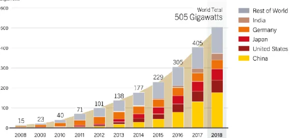
Figure I. 2. Solar PV global capacity by country and region, 2008 – 2018. Data are provided in
direct current (DC). From [15].
The evolution of the installed solar PV global capacity over the last decade can be seen in Figure I. 2. It reveals that the PV market is rapidly growing, with a cumulative capacity of 505 GW in 2018 as compared to only 15 GW ten years earlier. The electricity production capacity of PV increased by 100 GW in 2018 owing to its improving competitiveness, which makes solar PV the fastest-growing energy technology [5], [15].
However, since 2016 the growth rate of the PV global capacity has stabilized. This results from a 15% decrease of China’s annual addition to its PV capacity in 2018 following a substantial reduction of subsidies from the central government, which was compensated on the global scale thanks to an increasing demand in Europe and in emerging PV markets that is correlated to price reductions [15], [16]. This indicates that the development of the PV market is tied to its competitiveness as well as government policies. In this regard, the next sections will analyze the competitiveness of the PV technology, but also the global trends toward the energy transition and the reduction of greenhouse gases emissions.
1.2.2. Competitiveness of the PV electricity production
A consistent and widely used method to determine the price of electricity produced from different energy sources is to assess their levelized cost of electricity (LCOE). It consists in a calculation of the average total cost to install and operate a given power-generating system divided by its total energy production.
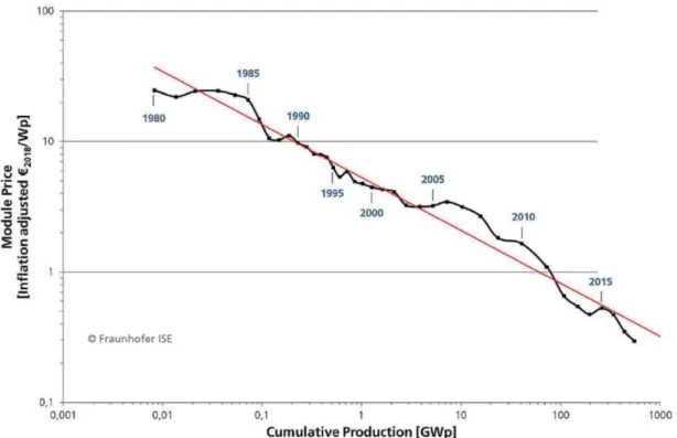
Figure I. 3. Price learning curve of solar PV modules, including all commercially available PV
technologies. From [5].
In 2018, the cost of a PV system ranged from 600 to 1400 €/kWp, depending on the PV technology and the type of PV plant, and the LCOE for PV systems varied between 3.71 and 11.54 €cent/kWh in Germany, based on the size of the PV installation and the average solar irradiance [17]. In comparison, the LCOE of coal lied between 4.59 and 9.96 €cent/kWh in 2018, depending on the coal quality and the type of power plant [17]. This means that PV is already a competitive source of electricity production.
The LCOE of PV systems decreased over the last years, essentially thanks to a reduction of the module prices [5], [17], as shown in Figure I. 3. A learning rate of 24% can be deduced from the price learning curve of the last 38 years, i.e. each time the cumulative production doubled, the module price decreased by 24%. On top of that, the cost of electricity generated from PV systems is also expected to decrease in the upcoming years. Using a learning rate of 15%, the LCOE of PV systems in 2035 is predicted to range between 2.16 and 6.74 €cent/kWh in Germany, while the LCOE of coal should be stable [17]. Thus, the competitiveness of PV should further improve over the years, confirming the strong growth potential of the PV market.
Nevertheless, the impacts of PV deployment are not limited to the economic field. Indeed, supplying energy and electricity from renewable sources has become a major challenge of the 21st century in order to reduce the emissions of greenhouse gases and to achieve a sustainable economy.
1.2.3. Climate change and greenhouse gases emissions
The issue of climate change has been gaining more and more attention over the past decades, and it can be considered as the next natural limit that our economy will have to face [2].
In this context, the Intergovernmental Panel on Climate Change (IPCC) has released five assessment reports since 1990, analyzing the impact of human activities on climate. The latest report underlines in particular the influence of anthropogenic emissions of greenhouse gases on climate change [1]. Figure I. 4 shows the upward trends in three greenhouse gases concentrations and in the annually and globally averaged surface temperature anomaly.
Figure I. 4. (a) Annually and globally averaged combined land and ocean surface temperature
anomaly. The temperature anomaly is derived from the difference between a given annual average temperature and the average temperature over the period with best coverage (1961 – 1990). Colors indicate different sources of data sets. (b) Atmospheric concentrations of three greenhouse gases: carbon dioxide (CO2, green), methane (CH4,
orange) and nitrous oxide (N2O, red), determined from ice core data (dots) and from direct
atmospheric measurements (lines). From [1].
Several factors allow to establish a relationship between human activities and climate change [2]:
• The use of fossil fuels and the deforestation due to mankind contribute to the increasing concentration of greenhouse gases in the atmosphere.
• Greenhouse gases are known to increase the average surface temperature on Earth by reflecting a part of the infrared light emitted from the ground.
• An uncontrolled global warming will have severe and irreversible impacts on both climate and economy.
Global awareness has raised on the topic of climate change. Government policies are more and more engaged toward the development of a sustainable economy and the reduction of greenhouse gases emissions, as shown recently with the ratification of
Conference (COP 21) [3]. It provides guidelines and a notable quantitative objective that all signing parties are committed to fulfill, as described in article 2(a):
Holding the increase in the global average temperature to well below 2°C above pre-industrial levels and pursuing efforts to limit the temperature increase to 1.5°C above pre-industrial levels, recognizing that this would significantly reduce the risks and impacts of climate change.
As of September 2019, the agreement was approved and signed by 185 countries [18], which is a major step toward the mitigation of climate change. To achieve the goal of a global average temperature increase limited to less than 2°C, the part of greenhouse gases emissions stemming from the production of electricity must be reduced.
Indeed, the sector of electricity production had the largest contribution to the emission of fossil fuel CO2 in 2014 [19]. The IPCC has also investigated various future scenarios up to 2100 in order to keep the temperature change due to anthropogenic greenhouse gases emissions below 2°C as compared to pre-industrial levels. In those scenarios, an atmospheric concentration of about 530 ppm CO2eq by 2100 is predicted to have a 50% chance of limiting the temperature change to 2°C [19]. The transition pathways of the electricity supply proposed in order to meet the goal of the Paris Agreement all show that the share of renewable electricity will strongly increase during the next decades, as seen in Figure I. 5. Interestingly, all scenarios exhibit a growth of the total electricity supply despite the decrease of the fossil fuel share in the production of electricity.
Figure I. 5. Transition pathways of electricity generation over the time span from 2010 to
2100 for mitigation scenarios that lead to atmospheric concentrations of greenhouse gases of 430–530 ppm CO2eq. From [19].
It is clear that renewable sources of electricity, including the PV technology, will play a major role in the upcoming energy transition. It is worth mentioning that the deployment of PV will also face several challenges, e.g. the uneven geographical availability and the intermittency of solar resources, the need for energy storage systems, the limited flow of energy that can be supplied from PV systems, and the toxicity of materials necessary to produce some types of PV modules [2]. Still, renewable energy sources, sunlight in particular, remain a promising alternative to carbon energy as they are abundant, various, and in general less polluting and dangerous than fossil fuels and nuclear power [2], [4]. In addition, a variety of PV technologies are already available and commercialized, which should bring more flexibility and resilience to the PV market and its electricity production. The next section will briefly describe the distribution of the PV market among those technologies.
1.3. Commercial PV devices: CIGS and other technologies
The solar PV market consists of several different technologies. The annual global production has been historically dominated by the silicon PV technology [5], which can be distinguished between monocrystalline and multicrystalline Si, as shown in Figure I. 6.(a). The share of multicrystalline Si has grown over the years to become the major technology for module production and represented 60.8 % of the annual production in 2017. In comparison, monocrystalline Si and thin film technologies accounted for 32.2% and 4.5% of the market in 2017 [5]. The proportion of thin film technologies in the annual production of modules is thus quite limited, and it has been regularly decreasing during the last decade.
Still, among thin film technologies the market share of CIGS modules has been the only one not to decrease since 2010, as it oscillated around 2% of the total PV module production [5]. Hence, the share of CIGS in the field of thin film technologies has increased up to approximately 42% in 2017, see Figure I. 6.(b). The rest of the thin film market is shared between CdTe and amorphous Si, with respective shares of 51% and 7%. Besides, as a result of the growing total PV production over the years, the production of CIGS modules has also been increasing to reach 1.9 GWp in 2017.
Figure I. 6. (a) Annual global PV production by technology (in GWp), from 2000 to 2017.
*2017 production numbers reported by different analysts may vary, a realistic total PV module production is estimated to be 97.5 GWp in 2017. (b) Annual global PV module production of thin-film technologies between 2000 and 2017. Data: from 2000 to 2010:
As of 2019, the record efficiency for a CIGS-based module is 17.4 ± 0.6 % (1.09 m2, aperture area), below the best efficiencies of 19.9 ± 0.4 % (1.51 m2, aperture area) for multicrystalline Si and 24.4 ± 0.5 % (1.32 m2, designated illumination area) for monocrystalline Si modules [6]. Still, the CIGS technology has several advantages for industrialization, even as compared to Si PV modules which largely dominate the market and benefit from their advanced commercial maturity [20], [21]:
• Thin film technologies rely on semiconductors with a direct bandgap and thus have a much higher absorption coefficient than Si which is an indirect bandgap material. As a result, thin film PV devices have low materials consumption as they require about 1 hundredth of semiconductor material as compared to Si. • CIGS modules exhibit a competitive LCOE as compared to multicrystalline Si, as
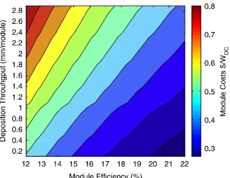
they were both calculated to range between 0.10 to 0.14 $/kWh for various locations in the US (2016) [7]. The LCOE of CIGS devices could be further reduced with a lower module price, an increased efficiency with a similar module price, and a reduced degradation rate [22].
• Thin film PV is well suited for building-integrated photovoltaics, thanks to the possible use of flexible substrate and the monolithic integration of modules. In addition, the CIGS technology is more robust than other PV materials under non-standard conditions of diffuse light, high temperature and partial shading. • Thin film PV has a carbon footprint of 12–20 g CO2eq/kWh, much lower than Si
with 50–60 g CO2eq/kWh due to its energy intensive purification and processing steps for fabrication. This contributes to the shorter energy payback time of 0.78 year for CIGS-based PV modules, instead of 2.12 and 1.23 years for mono- and multi-crystalline Si, respectively (assuming that modules are produced in China and installed in a region with a solar irradiation of 1700 kWh.h.m-2 per year) [23].
The present PhD thesis is focused on the reduction of absorber materials usage for the fabrication of CIGS-based PV devices. Doing so while successfully maintaining their efficiency would result in an improved competitiveness. Before analyzing the consequences of a reduced CIGS absorber thickness, the architecture and the physics of standard CIGS-based solar cells will be described in the next section.
Physics of CIGS solar cells
2.1. Introduction
In order to introduce the physics of CIGS PV devices, the typical architecture of CIGS-based solar cells will be presented together with a brief state of the art. The fundamental mechanisms for charge carrier generation and collection will be exposed. In addition, the main figures of merit that are commonly used to characterize and compare solar cells will be detailed.
2.2. CIGS solar cell architecture
The CIGS technology has been studied for more than 40 years. Back in 1975, the Bell laboratories reported an efficiency of 12%, which was measured outdoor under a solar intensity of ~92 mW/cm2 [24]. Since then, CIGS-based solar cells have been continuously improved and reached efficiencies over 20% at the laboratory scale in 2011 [25]. The record efficiency at present is as high as 23.35%, and was achieved by SolarFrontier [26].
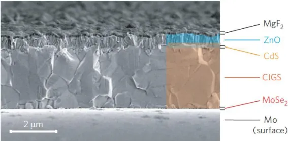
The standard architecture of a CIGS solar cell is depicted in Figure I. 7. CIGS photovoltaic devices are fabricated on a substrate, usually a slab of soda-lime glass, with a molybdenum layer as a back contact with the CIGS semiconductor. The front layers that complete the solar cell generally consist of a CdS buffer layer and ZnO-based transparent electrodes. In this configuration, light enters the solar cell stack from the top Al-doped ZnO layer. To reduce the total light reflection of the device, an additional antireflection coating made of MgF2 can be deposited on top of ZnO:Al.
Figure I. 7. Schematic of a standard CIGS-based solar cell.
The main properties and historical improvements of each layer will now be discussed. 2.2.1. Substrates
Soda-lime glass (SLG) is a type of glass that contains significant amounts of sodium, calcium and aluminum oxides beside silicon oxide. It is well suited as a substrate for the fabrication of CIGS solar cells, essentially thanks to:
• its low cost. The manufacturing cost for using a SLG substrate as well as a front stack of EVA/SLG is estimated to amount to ~12 $2015/m2 assuming a monolithic CIGS module fabricated by sputtering and sulfurization after selenization, for a 1 GW/year production volume in the U.S [7]. This represents only ~17% of the total module cost of 69 $2015/m2.
• its glass transition temperature in the 550–600 °C range [27] that is compatible with the typical deposition temperatures of CIGS.
• its thermal expansion coefficient of 9.1–9.5 × 10⁻⁶ K–1 [27], [28], that matches the one of the CIGS layer.
• the diffusion of Na from the SLG to the CIGS layer during the fabrication process. The incorporation of Na was reported to be beneficial for the performance of CIGS solar cells back in 1993 [27]. This aspect will be discussed together with the CIGS absorber in section I.2.2.3.
Recently, flexible substrates have also gained attention as they allow for a wider range of applications and cost-efficient roll-to-roll manufacturing processes [29]. A high efficiency of 20.8% was recently reported for a CIGS solar cell with an area of 0.5-cm2 on a polyimide substrate [30]. MiaSolé also reached an efficiency of 17.4 ± 0.6 % for a flexible CIGS module (1.09 m2, aperture area) [6].
2.2.2. Molybdenum and other back contacts
Mo is widely used as a CIGS back contact, and CIGS solar cells with the highest efficiencies include a Mo back contact deposited by sputtering [26], [31], [32]. Indeed, Mo is one of the few metals that is inert during the deposition of CIGS [33], and permeable to Na diffusion [27]. It also forms an ohmic contact with CIGS, in particular thanks to the growth of a MoSe2 [34] interfacial layer when Mo is exposed to Se vapor at temperatures ≥400°C [35].
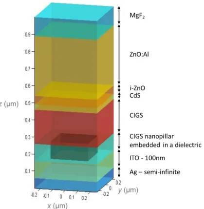
The fabrication of CIGS solar cells with transparent back contacts has also been investigated, in particular for bifacial applications [36], [37] or in superstrate configuration [38], [39], where light enters the solar cell respectively from both sides or from the substrate/back contact side. Transparent back contacts are usually made of a highly doped, transparent conductive oxide (TCO). The challenges and potential benefits of a transparent back contact – especially in the case of ultrathin CIGS absorbers – will be detailed in section I.3.2.3.
2.2.3. CIGS-based absorber
Cu(In,Ga)Se2 is a quaternary I-III-VI semiconductor. It can be regarded as an alloy of the CuInSe2 and CuGaSe2 ternary compounds, where In and Ga share the same atomic sites in the CIGS crystalline structure. The tetragonal chalcopyrite structure of CIGS is represented in Figure I. 8.
Figure I. 8. Schematic of the unit cell of the Cu(In,Ga)Se2 chalcopyrite crystalline structure,
where a and c refer to the lattice constants. From [40].
A distortion of the structure results in a ratio of lattice constants c/a ≠ 2, which depends on the composition in In and Ga. The lattice constants decrease from a = 5.780 Å and c = 11.604 Å for CuInSe2, to a = 5.607 Å and c = 10.983 Å for CuGaSe2 [41]. The atomic ratio of In and Ga in the CIGS composition, commonly denominated as GGI = [Ga]/([Ga]+[In]), also modifies the bandgap of CIGS following the formula [42]:
𝐸𝑔 = 1.01 + 0.626 × 𝐺𝐺𝐼 − 0.167 × 𝐺𝐺𝐼(1 − 𝐺𝐺𝐼) (I. 1)
A valence band offset of ΔEV = -0.04 eV and a conduction band offset of ΔEC = 0.60 eV between CuInSe2 and CuGaSe2 were calculated and reported by Wei and Zunger [43]. Highest efficiencies of CIGS solar cells are obtained for bandgap values close to 1.15 eV [32], [44], i.e. for average GGI ratios close to 0.30.
The Cu stoichiometry of CIGS solar cells, which can be expressed as the atomic ratio CGI = [Cu]/([Ga]+[In]), is generally below unity [30], [45]. The Cu deficiency of CIGS solar cells results in the formation of a compensated pair of shallow defects: (2𝑉𝐶𝑢 − − 𝐼𝑛𝐶𝑢2+) [46], while Cu-rich CIGS films exhibit significantly lower concentrations of defects [45]. Still, a slight prevalence of the Cu vacancy defects leads to a p-type doping of CIGS layers with Cu-poor stoichiometry [46]. A Cu-poor stoichiometry also improves the performances of CIGS solar cells thanks to the formation of ordered vacancy compounds (OVC) at the front interface of CIGS, such as Cu(In,Ga)3Se5 or Cu(In,Ga)5Se8 [47]. Indeed, the OVCs show a wider bandgap due to a lower valence band maximum as compared to the chalcopyrite CIGS [48]. Besides, the OVCs favor the diffusion of Cd deposited by chemical bath deposition (CBD), which can lead to a n-type doping of the OVC layer if Cd atoms are sufficiently activated [47]. These combined effects in turn repel holes toward the CIGS bulk and reduce recombination of charge carriers at the CdS/CIGS hetero-interface [45], [47].
As the presence of the OVC layer is necessary to reach high CIGS solar cell performances, the most common processes for the deposition of CIGS were designed to achieve high quality films with Cu-poor compositions. Two methods in particular are used for commercial manufacturing of CIGS modules: the co-evaporation process where absorber elements are simultaneously evaporated, and the sequential process in which metallic precursor layers are selenized or sulfoselenized under annealing [49]. The co-evaporation process, which was used in this work, was initially based on the growth of a bilayer [50], [51], but then evolved into the so-called three-stage process [52], [53] that consists in a Cu-poor/Cu-rich/Cu-poor growth sequence. The main benefit of this co-evaporation process is to enable the formation of a double-graded Ga composition, and thus a double-double-graded conduction band, that is beneficial to photovoltaic performances [29], [52], [54]. The impacts of the CIGS band grading will be further discussed in section I.3.2.1.
Figure I. 9. Cross-section image of a complete CIGS solar cell in scanning electron microscopy
(SEM). The device was fabricated on a polyimide substrate and achieved an efficiency higher than 18%. From [29].
Recently, a lot of research efforts have been made toward the incorporation of alkali to the CIGS absorber, as the coincidental diffusion of Na from the SLG substrate to the CIGS absorber was discovered to boost solar cell efficiencies in 1993 [27]. Indeed, Na in concentrations of ~1019 atoms/cm3 was shown to substitute the detrimental 𝐼𝑛
𝐶𝑢 2+ donor defect, thereby increasing the effective hole density of CIGS and reducing the recombination of charge carriers [27], [55]. Various strategies for the intentional incorporation of Na to CIGS have then been reported, such as the deposition of a NaF precursor layer on the back contact prior to CIGS deposition [56], [57], the use of a NaF post-deposition treatment (PDT) after the CIGS growth [58]–[60] and the fabrication of CIGS solar cells on Na-doped Mo back contacts (Mo:Na) [61]. Similar or improved efficiencies are achieved when Na is intentionally added to CIGS as compared to when it is incorporated via its out-diffusion from the SLG [57], [60]. This allowed in particular the development of efficient CIGS solar cells fabricated on Na-free flexible substrates like polyimide (PI) [29], [30], [62] or stainless steel foils [63], [64].
The addition of heavier alkali elements has also gained a lot of attention since 2013, when the record cell efficiency was achieved on a polyimide substrate with a KF PDT [65]. Contrary to Na, the incorporation of K during the growth of CIGS was reported to lead to the formation of a deep defect level that results in a reduced minority carrier lifetime and a poorer collection of photogenerated charge carriers [66]. In contrast, adding K to the CIGS layer via a PDT was shown to modify the composition of the CIGS front interface: it forms a K-containing In2Se3 compound in the OVC layer [67]–[70], and it enhances the formation of CdCu donor sites during the chemical bath deposition of the CdS buffer layer [65], [71]. As a result, the CdS buffer layer can be thinned to reduce its parasitic absorption, in turn improving the efficiency of CIGS solar cells [65]. The recombination rates at the heterojunction and in the depletion region were also shown to be reduced thanks to a K-treatment [72]. For a detailed summary of the effects associated with the PDT of KF, the reader can refer to the review from Muzillo [73]. Finally, heavier alkali elements like Rb and Cs were also studied recently, and led to the best CIGS efficiencies in particular thanks to improved carrier lifetimes. [26], [31], [32].
It is worth mentioning that alkali elements were reported to exhibit a heterogeneous distribution in CIGS, as they preferentially accumulate at grain boundaries and interfaces rather than in the CIGS grain interior [74]–[76]. However, the effects of alkali on the grain boundaries of CIGS are still debated, as recent studies reported either the existence or the absence of a grain boundary passivation effect due to the segregation of alkali [77], [78]. Nevertheless, CIGS layers generally exhibit micrometer-scale grains and thus a large amount of grain boundaries, as shown in the scanning electron microscopy (SEM) cross-section in Figure I. 9. The CIGS grain boundaries do not have a significant impact on solar cell performances [79] as they usually exhibit surface recombination velocities below 104 cm/s [78], [80], [81], which is estimated to be low enough to reach efficiencies over 20% [82].
Over the last 10 years, solar cells with high performance have also been achieved with absorbers based on silver-alloyed CIGS, i.e. (Ag,Cu)(In,Ga)Se2 (ACIGS), where Ag and Cu share the same atomic sites in the chalcopyrite structure [83], [84]. Regardless of the GGI ratio, the substitution of Cu by Ag results in a decreased melting temperature, an enhanced grain size and an increased bandgap with lower valence band and conduction band edges [84]–[86]. The lower melting point of ACIGS can decrease the amount of structural disorder thanks to a sintering effect, which could possibly reduce the density of intra-grain defects [86], [87]. Besides, the efficiency of CIGS solar cells with high GGI ratios and bandgaps over 1.3 eV can be improved with Ag-alloying, mostly thanks to the electronic band structure of ACIGS that allows a better band alignment with CdS as compared to CIGS [84], [88], [89]. Owing to the promising properties of this semiconductor, the development of ultrathin absorbers made of ACIGS was also investigated in this work.
2.2.4. Cadmium sulfide and buffer layers
Standard CIGS solar cells are fabricated by deposition of an n-doped CdS buffer layer on top of the CIGS absorber, thereby forming a p-n heterojunction. The CdS layer is usually grown by chemical bath deposition (CBD) in an aqueous solution of ammonia
containing a cadmium salt and a sulfur precursor like Cd acetate and thiourea, respectively [90].
The CBD process leads to the growth of conformal CdS layers that avoid detrimental shunt paths and protect the absorber surface from plasma damage during the deposition of the front contact layers by sputtering [91]. It was also reported that the diffusion of Cd in the OVCs at the front surface of the absorber could contribute to the passivation of the heterojunction interface [47]. However, the CdS buffer exhibits two major disadvantages: the toxicity of cadmium, and its rather low bandgap (~2.4 eV) that results in parasitic absorption at wavelengths below ~500 nm [91].
This led to the recent investigations of based buffer layers like Zn(O,S) [91]. Zn-based buffer layers are non-toxic, and can be deposited with a variety of processes including CBD [91], [92]. In addition, Zn(O,S) has a higher bandgap than CdS that can be tuned between 2.8 eV and 3.8 eV, depending on its oxygen and sulfur composition [93]. This feature notably allows a better band alignment and a proper conduction band offset at the heterointerface of wide bandgap CIGS-based absorbers [94].
It is worth mentioning that the current record efficiency for laboratory-scale CIGS solar cells of 23.35% was achieved with a Cd-free architecture, where the buffer layer consists of a Zn(O,S,OH)X film prepared by CBD [26].
2.2.5. Transparent front contact
The transparent front electrode is made of TCO films that combine a high transparency with a sufficient lateral conductivity. It is commonly prepared by sputtering of a bilayer stack made of intrinsic and aluminum-doped ZnO (i-ZnO/ZnO:Al).
The main role of the high-resistance i-ZnO film is to passivate pinholes in the CdS layer and to avoid local shunt paths in complete devices [90], [95]. The highly doped ZnO:Al layer ensures the lateral conduction of free electrons thanks to its low sheet resistance, which is typically in the order of magnitude of 10 Ω/sq. However, the ZnO:Al layer is also responsible for parasitic absorption in the infrared region due to free carrier absorption. Hence, its thickness has to be optimized to achieve both a sufficient transparency and conductivity.
CIGS devices with best efficiencies (>22 %) are prepared with highly transparent front contact layers, where i-ZnO is replaced by (Zn,Mg)O as its wider bandgap results in an increased transparency and provides a better band alignment with Zn(O,S) [26], [72], [96]. In addition, the top ZnO:Al layer can be replaced by a more transparent boron-doped ZnO film [26], [32], [97].
2.2.6. State of the art for CIGS devices
Table I. 1 gives a brief overview of the best efficiencies that were reported for CIGS-based solar cells and modules. To compare the performances of CIGS devices with other photovoltaic technologies, one may refer to the record efficiency tables edited by Green et al. [6].
For a deeper understanding of the CIGS-based photovoltaic technology, the next section will detail the physics of CIGS solar cells.
le I . 1 . S ele cti on of hi gh -per for m in g CIG S-ba se d sola r cell s an d m odu les th at w ere rec ent ly ac hi eve d. * Indepe nden tly ce rt ifi ed eff ic ienc ie s. Institute o r comp an y Sub str ate & ba ck c on ta ct CIG S de positi on me thod B uffe r la ye r Fr on t c on ta ct Eff ic ie nc y & ar ea R efe re nc e Solar c el ls ar F ro ntie r G la ss / M o Sp utte ri ng, s el en iza tion the n sul fur iza tion , a nd Cs post -tr ea tme nt Zn (O,S ,OH) X Zn 0.8 Mg 0.2 O / Zn O:B 23.35 % * (1.04 cm 2) [26] ar F ro ntie r G la ss /M o Sp utte ri ng, s el en iza tion the n sul fur iza tion , a nd C s post -tr ea tme nt CdS no in tr in sic la ye r Zn O:B 22.9 % * (~1 cm 2) [32] ZSW G la ss /M o Co -e va por ation , R bF PDT CdS (Z n,M g) O or i-Zn O / Zn O:Al 22.6 % * (~0.5 cm 2) [31] Uppsa la Unive rs ity G la ss /M o Co -e va por ation of A CIG S CdS i-Zn O/ Zn O:Al 20.9 % (~1 cm 2) [84] EM PA PI/ M o Co -e va por ation a t 450°C, R bF PDT a nd ca ppin g la ye r CdS i-Zn O/ Zn O:Al 20.8 % * (0.52 cm 2) [30] N R EL SL G /M o Co -e va por ation CdS i-Zn O/ Zn O:Al 20.8 % * (~0.1 cm 2), 23.3 % * co nc en tr ate d [98] Mo d u les M ia Sol é Sta in le ss ste el /M o:N a Sp utte ri ng an d se le niza tion CdS (s putte ri ng) ? / Zn O:Al 17.4 % * (1.09 m 2) [96], [9 9] Sol ib ro G la ss /M o Co -e va por ation CdS i-Zn O/ Zn O:Al 17.5% * (0.94 m 2) [96] A va nc is G la ss /SiN /Mo Sp utte ri ng, r apid the rma l p roc es sin g, S an d Se Zn (O,S ) Zn O:Al 19 .0 % (0.67 cm 2) [100]
2.3. Charge carrier generation
The fundamental principle of a photovoltaic device is to generate electrical power by absorbing light in order to generate positive and negative charge carriers, and to selectively extract them at two distinct contacts [101]. In practice, this is usually achieved via a p-n junction of two semiconductor materials, though it is not an absolute requirement for an efficient solar cell [101], [102]. The sun provides an abundant, quasi-unlimited source of light that can be converted into power by photovoltaic systems [4], which is why they are generally designed to produce electricity from sunlight. Hence, the solar spectrum will first be described in this section, then the absorption of light and generation of charge carriers will be analyzed. Finally, the collection of charge carriers as well as the main loss mechanisms will be presented together with the common performance parameters.
2.3.1. The solar spectrum
Figure I. 10 shows the solar spectral irradiance received on Earth which was modeled with the SMARTS2 (version 2.9.2) software [103]. Two reference conditions are described, the spectral irradiances for an air mass of 0 and 1.5, respectively designated as AM 0 and AM 1.5 G:
• The AM 0 spectrum corresponds to the extraterrestrial spectral irradiance, at the surface of the Earth’s atmosphere. It is close to the spectral irradiance of a black body at 5800 K, which describes quite accurately the light spectrum emitted by the Sun [102].
• The standard global AM 1.5 spectral irradiance is the fraction of the solar spectrum that reaches a surface on Earth under normal incidence conditions, for an elevation of the Sun of 41.8° above the horizon. More simply put, it is the solar spectral irradiance that impinges the terrestrial surface after crossing the atmosphere over a distance corresponding to 1.5 times its thickness [103]. The “global” spectrum (AM 1.5 G) takes into account the typical diffusion of the atmosphere. It exhibits absorption bands due to molecules found in the atmosphere, such as O2, CO2, H2O and others. The standard testing conditions (STC) for one-sun illumination uses the AM 1.5 G spectrum as a reference. Its integrated irradiance leads to a power density of ~1000 W.m-2.
The filled area represents the maximum solar power density of the AM 1.5 G spectrum that can be converted into electrical power by a CIGS-based solar cell with a standard bandgap of 1.15 eV, or ~1080 nm when expressed as a wavelength. In this respect, the two major loss mechanisms of photovoltaic energy conversion are unfolded: the non-absorption and the thermalization of photons whose energy is respectively lower and higher than the bandgap of the absorber, or alternatively photons with wavelengths above and below the wavelength corresponding to the bandgap, respectively. These unavoidable loss processes, as well as radiative recombination and isothermal dissipation losses occurring in photovoltaic devices can be described with the well-known Shockley-Queisser model [104], using the thermodynamic principle of detailed balance. A discussion of this theoretical efficiency limit can be found in [101]. For the typical bandgap range of CIGS solar cells (1.1–1.3 eV), a maximum efficiency of ~33% is predicted under STC [105].
Figure I. 10. Solar spectral irradiance for an air mass of 0, i.e. outside the Earth’s atmosphere
(AM 0, black line), and standard global spectral irradiance reaching the Earth’s surface for an air mass of 1.5 (AM 1.5 G, red line). The filled area is the sunlight power density (AM 1.5 G) that can be converted by a CIGS solar cell with a typical bandgap of Eg = 1.15 eV, taking
into account thermalization losses.
In conclusion, the first requirement that must be considered to achieve an efficient photovoltaic device is the absorption of the incident light over a wide range of wavelengths.
2.3.2. Light absorption
Semiconductor materials, unlike metals, exhibit electronic band structures with a bandgap (Eg), which is an energy range where no electron states can exist. In the fundamental state, i.e. without any excitation, the electronic band at the lower energy edge of the bandgap is filled with electrons and is called the valence band. On the other hand, the electronic band at the upper energy edge of the bandgap is depleted of electrons and is referred to as the conduction band. The semiconductor can thus be considered as a two-level system. Figure I. 11 depicts how an incident photon can interact with this two-level system in three distinct ways depending on its energy ℎ𝜈: 1. ℎ𝜈 < 𝐸𝑔, the photon energy is lower than the bandgap. In this case the photon is not absorbed by the semiconductor and will not be converted by the solar cell.
2. ℎ𝜈 = 𝐸𝑔, the photon energy is equal to the bandgap. For this situation, the photon can be absorbed by the semiconductor, as it provides a sufficient energy to promote an electron from the valence band to the conduction band, leaving a positively-charged empty state in the valence band that is commonly called a hole. This mechanism results in the creation of an electron-hole pair without any energy loss.
500 1000 1500 2000 2500 0.0 0.5 1.0 1.5 2.0 Sp ectral Irr adianc e (W.m -2 .nm -1 ) Wavelength (nm) AM 0 AM 1.5 G Fraction of the AM 1.5 G spectral irradiance that is convertible by CIGS solar cells (Eg = 1.15 eV) Typical CIGS bandgap
3. ℎ𝜈 > 𝐸𝑔, the photon energy is higher than the bandgap. In this configuration, the photon can also generate two carriers but the excess energy is relaxed on a sub-picosecond timescale due to the emission of phonons and the thermalization of the carriers to the band edges [101]. Hence, the maximum energy that can be converted from photons whose energy is higher than the semiconductor’s bandgap is limited, see also Figure I. 11.
Figure I. 11. Schematic representation of the different interactions between a photon and a
two-band system. If ℎ𝜈 < 𝐸𝑔, the photon is not absorbed. If ℎ𝜈 = 𝐸𝑔 the photon can promote an electron from the valence band to the conduction band with no energy loss in the process. If ℎ𝜈 > 𝐸𝑔, the photon can also generate a pair of charge carriers, but the excess energy ℎ𝜈 − 𝐸𝑔 is lost by thermalization of the electron and hole to the band edges EC and EV,
respectively.
2.3.3. Generation of charge carriers
The simple presentation of the photon absorption in the previous section describes the relationship between light absorption of a semiconductor and its bandgap. In addition, the absorption coefficient of a semiconductor is a wavelength-dependent function that is related to the electronic band structure of the semiconductor. Semiconductors with a direct bandgap, like CIGS and other absorbers of the thin-film photovoltaic technology, exhibit a much higher absorption coefficient than Si, which has an indirect bandgap that requires phonon-photon interactions for light absorption. In practice, some of the incident photons with an energy higher than the semiconductor’s bandgap are not absorbed, due to light reflection out of the device or parasitic light absorption in inactive layers for example.
Figure I. 12 shows the absorption coefficient of CIGS for a bandgap of 1.2 eV and the density of the generated charge carriers for a solar cell with a 1000 nm-thick CIGS layer under one-sun illumination. Most of the charge carriers are generated close to the CdS buffer layer, within a CIGS depth of about 500 nm. Some interferences with a small amplitude are observed at the CIGS back contact due to light reflection at the CIGS/Mo back contact. In this case, a non-negligible part of the incident light is transmitted to the metallic Mo back contact. It is absorbed in the Mo layer but it does not contribute to the generation of electron-hole pairs, because the charge carriers get completely thermalized in the continuous electronic band structure of the metal.
Figure I. 12. a) Absorption coefficient of CIGS for a bandgap of 1.2 eV derived from
ellipsometric measurements and b) profile of the generated charge carrier density in a 1000 nm-thick CIGS layer, simulated for a CIGS solar cell under one-sun illumination with the ray transfer matrix method. From [12].
In order to produce an electrical power with a solar cell, the charge carriers generated in the semiconductor material need to be selectively collected before they recombine. The collection of charge carriers will be analyzed in the next section for the case of the CIGS/CdS heterojunction.
2.4. Charge carrier collection
2.4.1. The p-n junctionIn most photovoltaic devices, a p-n junction is designed to achieve an efficient collection of the photogenerated charge carriers. In the case of the CIGS technology, the p-n junction consists in a heterojunction formed between 2 semiconductors of different bandgaps: CIGS and CdS. In Figure I. 13, the electronic band diagram of a typical CIGS solar cell under one-sun illumination at short-circuit condition was simulated with SCAPS (version 3.3.07, software created by Burgelman et. al from the university of Gent [106], [107]), with materials parameters described in [29].
Discontinuities, or offsets, of the valence band maximum and the conduction band minimum are observed due to the varying bandgap of each material constituting the solar cell. Besides, the contact between the p-doped CIGS and the n-doped CdS results in the formation of a built-in potential. For a detailed derivation of this potential and associated electric field, the reader may refer to the work of Prof. Würfel [102]. As the CIGS layer is poorly doped (acceptor density 𝑁𝐴 = 4 × 1015 cm-3) and the CdS is highly doped (donor density 𝑁𝐷 = 1 × 1018 cm-3), the neutrality condition at the CIGS/CdS interface results in a depletion of free carriers in the CIGS region over a depth of approximately 300 nm, which is called the Space Charge Region (SCR). In the rest of the CIGS layer, the density of majority carriers (holes) and the net doping density are almost equal (𝑝 ≈ 𝑁𝐴). Hence, this portion of the CIGS film is almost neutral and is designated as the Quasi Neutral Region (QNR).
Figure I. 13. SCAPS simulation of the band diagram of a CIGS solar cell under one-sun
illumination at short-circuit condition (V = 0). Materials parameters used for in the simulation model were taken from [29]. The CIGS composition is fixed at GGI = 0.3, corresponding to a bandgap of Eg = 1.16 eV.
The charge carriers generated in this structure migrate with respect to the diffusion and drift processes and can be selectively collected at each interface. The following section will present the mechanisms leading to charge collection.
2.4.2. Diffusion and drift mechanisms
Two distinct processes are responsible for the motion of photogenerated charge carriers in the CIGS solar cell:
• The diffusion mechanism tends to equilibrate the densities of free carriers. As a consequence, the majority carriers of CdS (electrons) diffuse to CIGS, and the majority carriers of CIGS (holes) diffuse to CdS. The resulting current densities are expressed as:
𝐽𝑛,𝑑𝑖𝑓𝑓 = + 𝑞 𝐷𝑛𝑑𝑛
𝑑𝑥 (I. 2)
𝐽𝑝,𝑑𝑖𝑓𝑓 = − 𝑞 𝐷𝑝𝑑𝑝 𝑑𝑥
• where x is the distance over single direction (one dimensional model), q the elementary charge, n and p the free carrier densities of electrons and holes, Dn and Dp are the diffusion coefficients of electrons and holes, respectively. The difference between the two populations of charge carriers can also be regarded as a chemical potential Δµ that corresponds to the quasi Fermi level splitting of electrons and holes, respectively Efn and Efp (see [102] for more information). The diffusion length of free carriers is linked to D and the carrier lifetime τ as follows: 𝐿 = √𝐷𝜏 (I. 3) 0.0 0.5 1.0 1.5 2.0 -3 -2 -1 0 1 E (eV) Depth (µm) EV EC Efn Efp CIGS CdS ZnO:Al QNR SCR ZnO Mo
• The electric field created across the junction drifts charge carriers, leading to the following drift current densities:
𝐽𝑛,𝑑𝑟𝑖𝑓𝑡 = 𝑞 𝑛 𝜇𝑛 𝑬
(I. 4) 𝐽𝑝,𝑑𝑟𝑖𝑓𝑡= 𝑞 𝑛 𝜇𝑝 𝑬
• where µn and µp are the mobilities of electrons and holes, respectively. The drift current dominates the motion of charge carriers in the SCR, sweeping electrons (respectively holes) toward CdS (respectively CIGS). As a result, an almost perfect collection of carriers can be assumed in the SCR thanks to its electric field. However, one must keep in mind that the width of the SCR is voltage-dependent, and is much reduced when a solar cell is operated at its maximum power point, as compared to the short-circuit condition (V = 0) [102]. The contribution of the drift currents is thus lower for operating solar cells.
The Gärtner model [108]–[110] can be used to describe the collection efficiency of a CIGS solar cell. In this model, the collection is assumed to be limited by the diffusion of minority carriers to the CdS layer. In addition, the back contact recombination of the CIGS layer is neglected, which is a valid approximation only for CIGS films much thicker than the electron diffusion length. The collection is considered to be perfect for carriers generated in the SCR region, as well as for carriers generated in the QNR region at a distance from the SCR that is below one electron diffusion length. This leads to a collection function of 𝑓𝑐𝑄𝑁𝑅
= exp (−(𝑥 − 𝑤)/𝐿𝑛), with w the space charge region width and Ln the electron diffusion length.
However, some of the photogenerated charge carriers recombine in the CIGS solar cell before being selectively collected, and recombination losses can in turn decrease the diffusion length of carriers. Hence, the various recombination processes need to be considered in order to accurately describe the collection of charge carriers in CIGS photovoltaic devices.
2.4.3. Recombination and other losses
CIGS solar cells undergo radiative band to band recombination (annihilation of an electron-hole pair with the emission of a photon) and non-radiative recombination. These recombination processes result in the following current-voltage or I(V) relationship for a solar cell in the dark:
𝐽𝑑𝑖𝑜𝑑𝑒 = 𝐽0(exp (𝑞𝑉/𝑘𝑇) − 1) (I. 5)
with Jdiode being the diode current density, also called dark current. J0 is the saturation current, q the elementary charge, k the Boltzmann constant and T the temperature. This diode current is dependent of the applied bias and recombination mechanisms taking place in the photovoltaic device. In the ideal case of a solar cell without non-radiative recombination, the saturation current J0 is only due to the non-radiative recombination of the solar cell with an emission spectrum that corresponds to a black-body with the temperature of the solar cell.