HAL Id: hal-00005013
https://hal.archives-ouvertes.fr/hal-00005013
Submitted on 21 Jun 2005HAL is a multi-disciplinary open access archive for the deposit and dissemination of sci-entific research documents, whether they are pub-lished or not. The documents may come from teaching and research institutions in France or abroad, or from public or private research centers.
L’archive ouverte pluridisciplinaire HAL, est destinée au dépôt et à la diffusion de documents scientifiques de niveau recherche, publiés ou non, émanant des établissements d’enseignement et de recherche français ou étrangers, des laboratoires publics ou privés.
GROWTH OF EPITAXIAL TUNGSTEN NANORODS
Marcel Gillet, Romain Delamare, Eveline Gillet
To cite this version:
Marcel Gillet, Romain Delamare, Eveline Gillet. GROWTH OF EPITAXIAL TUNGSTEN NANORODS. Journal of Crystal Growth, Elsevier, 2005, volume 279, issues 1-2, p 93-99. �10.1016/j.jcrysgro.2005.01.089�. �hal-00005013�
Growth of epitaxial tungsten oxide nanorods
M.Gillet*, R. Delamare, E. Gillet
UNIVERSITE D’AIX-MARSEILLE – L2MP-UMR CNRS 6137 Faculté des sciences et techniques – case 151
52 Avenue Escadrille Normandie Niemen, 13397 Marseille cedex 20, France
Abstract
A simple vapour deposition technique was used to prepare WO3 one-dimensional
nanostructures. WO3 is sublimated at a relatively low temperature (550°C) in air at
atmospheric pressure. The sublimated species are condensed on mica substrate at 500°C. Single crystalline are grow in epitaxy on the mica surface with a growth axis along [010] directions and (001) plane parallel to the substrate. A growth process is proposed in which the formation of a one-dimensional tetragonal tungsten bronze as precursor is the determinant factor.
Keywords
A1: Nanostructures, A2: Growth from vapor, B1: Nanomaterials, B1:Oxides.
Introduction
Tungsten oxide has been widely studied and used in applications such as catalysis [1] electrochromic devices [2, 3, 4] or gas sensors [5, 6, 7]. Tungsten oxide WO3 is a n type
semiconductor with interesting properties as sensing material and recently it has been shown that nanostructured thin films have superior sensitivity compared to those of bulk material [8, 9]: Various methods including chemical vapour deposition [10], electrochemical deposition [11], laser vaporisation [12, 13] have been used to prepare tungsten oxide thin films. In conventional WO3 thin films with nanoscale size grains, the electrical conduction is mainly
controlled by the free carrier transport across the grain boundaries. So the synthesis of monocristalline tungsten oxide as nanowires or nanorods is of great interest. In the past years few papers have been devoted to the growth of such one dimensional nanostructure. Y.Z. Zhu
[14] produced micrometer scale tree-like structure by heating a tungsten foil, partly covered by SiO2 in Ar atmosphere at 1600°C. Theses nanostructures were composed by monoclinic
W18O49 nanoneedles and by WO3 nanoparticles. Nanorods of several oxides including WO3
have been prepared by templating on acid-treated carbon nanotubes [15]. By heating WS2 in
oxygen, fibers of W18O49 were produced with a pine-tree like structure [16]. Mixtures of WO2
and WO3 with nanorods structure were obtained by koltyptin et al [17] via amorphous
tungsten oxide nanoparticles. Y.B. Li et al [18] have synthesized WO3 nanobelts and
nanorods via physical vapour deposition process where the nanostructures were deposited on silicium wafers maintained at 600°C. Recently Z. Liu et al [19 ] reported on the preparation of tungsten oxide nanowires through a vapour-solid growth process by heating a tungsten wire partially wrapped with boron oxide at 1200°C and Y. Shingaya et al. [20] prepared by oxidation at high temperature well oriented WOx nanorods on a (001) W surface.
In this paper we report on the formation of tungsten oxide by a simple method using a vapour-solid growth process. Tungsten oxide is sublimated from a predeposited WO3 layer and
condensed on a mica substrate. A growth process is proposed where the formation of a tetragonal tungsten bronze acts as a precursor for the epitaxial growth of the nanorods.
Experimental procedure
Figure 1 shows the experimental set up that we have used to produce tungsten oxide nanorods. The tungsten oxide vapour source is a tungsten oxide thin layer predeposited on a SiO2 substrate heated at a temperature T1 by an electrical heater. The WO3 vapour condenses
on a substrate located above the vapour source at a distance d of the source by means of a wedge made in silicon. The temperature T1 and the distance d determine the substrate
controlled. In the our experiments T1 was fixed to 550°C, and the resulting value of the
substrate temperature T2 was 450° ±10°C.
We have used (0001) mica, (0001) Al2O3 and SiO2 surfaces as substrates. Depositions were
performed at atmospheric pressure in air with a degree of humidity comprise between 30 and 40%. After cooling at room temperature the substrate surface above the source had a faint yellow colour. The deposits were examined on their substrates by Atomic Force Microscopy (AFM). The structure of nanorods was investigated by High Resolution Transmission Electron Microscopy (HRTEM) and Transmission Electron Diffraction (TED). For electron microscopy observations a carbon replica was deposited on the sample surfaces and stripped off in water. The transfer replica contained a number of nanorods well suitable for TEM and TED investigations.
Results
The AFM observations showed that tungsten oxide nanorods grown on a mica substrate. On Al2O3 and SiO2 substrates, only three-dimensional aggregates were observed.
Experiments in air with various degrees of humidity have shown that WO3 nanorods can be
obtained in air with humidity in a range of 10-40%. Figure 2a is a typical AFM image obtained of a mica substrate after 45 minutes deposition time. It shows nanorods grown along the substrate with well defined directions. One or two nanorods orientations are predominantly observed. The tungsten nanorods size depends on the deposition time but for a given deposition time the size is not uniform. However the length seems to be independent of the deposition time while the width and the thickness increase with as illustrated by the figure 2b corresponding to a deposition time of 60 min. In our experiments the deposition time varied between 10 and 90 mn. The nanorod dimensions vary in ranges 1-15µm, 10-200nm and 1-50nm for the length, width and thickness, respectively. The observed nanostructures
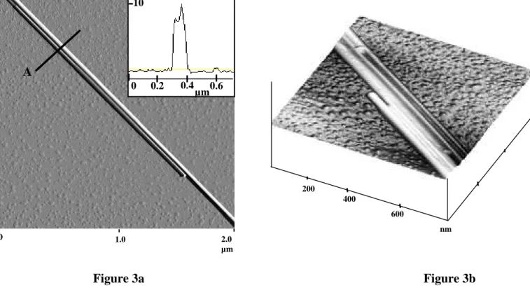
often exhibit multiple rods with twinned parts. Figure 3a shows as example such a double rod with one part grown in twin position. As the deposition time increases multitwining occurs as shown on figure 3b.
As mentioned in the experimental procedure, for electron microscopy investigations, the nanorods are extracted from their substrate by a transfer replica and observed without the mica substrates. The Energy Dispersive Xray Spectroscopy (EDX) shows that the nanorods contain potassium atoms (figure 4). Whatever their thickness the observed nanorods have approximatively the same amount of potassium as deduced from their EDX spectrum. We suppose that the nanorods grown on mica are initially composed of tungsten bronze (KxWO3)
Figure 5 and 7 illustrate two types of ED patterns from nanorods with two different thicknesses. The nanorod of figure 5 is a typical ED pattern of a thin nanorod e ≅3nm with a rectangular basic cell the interatomic distances as deduced from the ED are d1=0.627nm d2=0.382nm. This pattern can be interpreted as due to an hexagonal tungsten bronze (HTB) with lattice dimensions a=b=6.25 Ǻ and c= 3.83 Ǻ. From the ED we deduced that the HTB crystals grown on the mica surface with a (100) plane parallel to the substrate. This HTB structure is illustrated by the HRTEM image of figure 6 corresponding to the ED of the figure 5. The enlarged part inserted in the figure 6 shows the rectangular unit mesh and indicates the atomic distance in a (100) plane parallel to the surface of the nanorod, the second kind of ED patterns observed on the nanorods is represented on the figure 7 which exhibits two kinds of diffraction spots: Spots with strong intensities correspond to lattice distances d200=0.367 nm Ǻ
and d020= 0.378 nm which are very close of the theoretical distance in bulk WO3 (dth 200=
3.653 and dth020=3.77) and spots with low intensities located at half the distance between the
bright spots. We interpret this electron diffraction pattern by the coincidence of two phases: a WO3 phase with a monoclinic structure (a= 7.29 Ǻ, b= 7.53Ǻ, c= 7.68Ǻ, β=90.91°) and a
monoclinic structure with [001] axis perpendicular to the substrate and a growth direction parallel to the [010] WO3 direction. The figure 8 shows a HRTEM image corresponding to the
ED of the figure 7. It exhibits a nearly square unit mesh characteristic of a (001) plane of the WO3 monoclinic structure. The dimensions of the unit mesh as measured on the HRTEM are
indicated on the enlarged parts inserted in the figure 8. According to these results we consider that in the first stage of growth, hexagonal tungsten bronze nanostructures epitaxially grow on the mica substrate and further growth lead to WO3 nanorods with a monoclinic structure.
Growth mechanism
The tungsten oxide nanorods grow from deposition of vapour containing WO3
generated at relatively low temperature, in air with a humidity degree which varies in a 20-40% range. Nanorods growth only takes place on mica substrate and in well defined orientations on the substrate. We propose a growth process based on these experimental results. It is known that many whiskers and nanowires are grown by a vapour-liquid-solid mechanism [21] in general perpendicular to the substrate and have a droplet on their tip [22]. In our experiments we did not observe droplet on the end of tungsten oxide nanorods, this indicates that the growth proceeds by a vapour-solid (VS) growth mechanism.
Experimental results show that the WO3 nanorods are grown from WO3 species sublimated in
air containing water vapour, considerably lower than the sublimation temperature of bulk WO3 (1470°C). We cannot exclude that the water vapour plays a role in the sublimation
process, according to a reaction:
WO3 + H2O → WO2 (OH) 2
On an other hand the nanorods do not grow on Al2O3 or SiO2 substrates but only on mica
substrates containing potassium ions in addition to the chemical elements present in Al2O3
growth is driven by the interaction between the species of the mica substrate and the deposit to form tungsten bronze KxWO3. Due to the role of the water vapour the following reaction:
WO2 (OH)2 + x K → KxWO3 + H2O seems the most probable.
Similar processes involving WO2( OH)2 species have been proposed in the growth mechanism
of K0.4WO3 whiskers via an hydrothermal process using WO3 as tungsten source, KOH as
potassium source and hydrazine hydrate as reducing agent [23].
In the potassium tungsten oxide bronze (KxWO3), the W atoms are octahedrally coordinated
with oxygen atoms to form WO6 octaedrons. The WO6 octaedrons join each other by shearing
oxygen corner atoms. Tungsten bronzes can adopt various types of structures depending on ionic radius of the incorporated metal atom and on the composition. Hexagonal tungsten bronzes (HTB) can be formed with K ions in the composition range 0.13<x<0.33. In the HTB the WO6 octaedrons form hexagonal tunnels where the potassium ions can be located.
So we suppose that an epitaxial HTB grow on the surface of the mica substrate and acts as a precursor for the further WO3 nanorod growth. The resulting monoclinic WO3 structure result
either of the growth of WO3 on the HTB or of the growth of an hexagonal WO3 followed by
the transition of the hexagonal structure to a monoclinic structure. Hexagonal tungsten oxide is metastable phase and transforms irreversibly into the monoclinic structure WO3. This
transformation has been studied in detail by M. Figlarz et al. [24]. From the AFM observations it seems that the WO3 growth proceeds layer by layer increasing the thickness
and the width of the nanorods. During the growth twinning occurs along the [010] direction of the nanorod. The two twinned nanostructures are tilted relative to each other by about 2β-180°
(monoclinic angle β = 90.91°). During the deposition the twinning can be repeated resulting
in a multi twinned nanorod as shown on AFM images (figure 3b) or on TEM image (figure 4b). Such twinning is a relative common feature in WO3 material. It has been observed by
LEED on monocristalline WO3 [ 24] and in WO3 grain in epitaxial WO3 thin film by ED [25 ]
resulting in diffraction spot splitting.
Conclusion
Tungsten oxide nanorods have been epitaxially grown on mica using a simple vapour solid growth process. Experiments on different substrates (Mica, Al2O3, and SiO2) have shown that
the presence of potassium atoms is determinant for the nanorods growth. We deduce a growth process involving the formation of a one dimensional tetragonal tungsten bronze epitaxially oriented on the mica. This tetragonal tungsten bronze is a precursor for the WO3 nanorod
growth. Its formation on the mica substrate determines the nanorod morphology and orientations.
Acknowledgements
The work is supported by the European contract “Nanostructures for chemical sensors” (Project of the sixth Framework Programme).
References:
[1] F.A. Cotton and G. Wilkinson In: Advances in Organic Chemistry (5th ed.), Wiley, New York, 1988, p.829.
[2] C.G. Granqvist. Sol. Energy Mat. Sol. Cells 60 (2000) 201.
[3] B.P. Jelle and G. Hagen. Sol. Energy Mat. Sol. Cells 58 (1999) 277.
[4] I. Turyan, U.O. Krasovec, B. Orel, T. Saraidorov, R. Reisfeld and D. Mandler. Adv. Mater. 12 (2000) 330.
[5] W.M. Qu and W. Wlodarski. Sens. Actuators, B 64 (2000) 42.
[6] K.H. Lee, Y.K. Fang, W.J. Lee, J.J. Ho, K.H. Chen and K.S. Liao. Sens. Actuators B 69 (2000) 96.
[7] E. Llobet, G. Molas, P. Molinas, J. Calderer, X. Vilanova, J. Brezmes, J.E. Sueiras and X. Correig. J. Electrochem. Soc.147 (2000) 776.
[8] J. Tamaki, A. Hayashi, Y. Yamamoto, M. Matsuoka, Sens. Actuators B 95 (2003) 111.
[9] M. Gillet, K. Aguir, M. Bendahan, P. Menneni, Accepted in Thin Solid Films. [10] E. Brescacin, M. Basato and E. Tondello. Chem. Mater. 11 (1999) 314.
[11] Z.R. Yu, X.D. Jia, J.H. Du and J.Y. Zhang. Sol. Energy Mat. Sol. Cells 64 (2000) 55.
[12] M. Sun, N. Xu, J.W. Yao and E.C. Wang. J. Mater. Res. 15 (2000) 927. [13] S.T. Li and M.S. El-Shall. Nanostruct. Mater. 12 (1999) 215.
[14] Y.Q. Zhu, W. Hu, W.K. Hsu, M. Terrones, N. Grobert, J.P. Hare, H.W. Kroto, D.R. M. Walton and H. Terrones, Chem. Phys. Letters 309 (1999) 327.
[15] B.C. Satishkumar, A. Govindaraj, M. Nath and C.N.R. Rao, J. Mater.Chem 10 (2000) 2115.
[16] W.B. Hu, Y.Q. Zhu, W.K. Hsu, B.H. Chang, M. Terrones, N. Grobert, H. Terrones, J.P. Hare, H.W. Kroto and D.R.M. Walton. Appl. Phys. A 70 (2000) 231. [17] Y. Koltypin , S. I. Nikitenko and A. Gedanken, J. Mater. Chem. 12 (2002) 1107. [18] Y.B. Li, Y. Bando, D. Golberg and K. Kurashina, Chem.Phys.Letters, 367 (2003) 214.
[19] Z. Liu, Y. Bando and C. Tang, Chem.Phys.Letters, 372 (2003) 179. [20] R.S. Wagner and W.C. Ellis. Trans. Met. Soc. AIME 233 (1965) 1053.
[21] H. Yumoto, T. Sako, Y. Gotoh, K. Nishiyama and T. Kaneko, J. Cryst. Growth 203 (1999) 136.
[22] X. Yang, C. Li, M.S. Mo, J. Zhan, W. Yu, Y. Yan, and Y. Qian, J. Cryst. Growth 249 (2003) 594.
[23] R.J.D. Tilley, Int. J. of Refractory and Hard materials 13 (1995) 93.
[24] F.H. Jones, K. Rawlings, J.S. Foord, R.G. Egdell , J.B. Pethica, B.M.R. Wanklyn, S.C. Parker, P.M. Oliver, Surf.Sci.359 (1996) 107.
Captions:
Figure 1: Experimental set-up of the WO3 deposition process. T1= substrate temperature,
T2=Temperature of the WO3 source, d= distance between the source and the substrate. · Figure 2: (a) AFM image of WO3 nanorods grown on mica. Deposition time: 45 mn.
(b) AFM image of WO3 nanorods grown on mica. Deposition time: 60 mn.
Figure 3: (a) AFM image of twinned nanorods. In inset: thickness profile according to the
cross section A
(b) AFM image of multi-twinned nanorods (Tridimensionnal view).
Figure 4: EDX spectrum of a WO3 nanorod. The elements corresponding to the various peaks
are indicated.
Figure 5: Electron diffraction pattern of a thin nanorod ( e≅ 3nm).
Figure 6: HRTEM image corresponding to the ED pattern of the figure 5. The unit mesh is
indicated on the enlarged part (inset).
Figure 7: Electron diffraction pattern of a WO3 nanorod ( thickness: 5nm).
Figure 8: HRTEM image corresponding to the ED pattern of the figure 7. The unit mesh is
indicated on the enlarged part (inset).
WO3 LAYER HEATER PREDEPOSITED SUBSTRATE WEDGE CONTROLLED ATMOSPHERE T1 T2 d Figure 1
-10.0 -7.5 -5.0 -2.5 -0 10.0 7.5 5.0 2.5 0 Figure 2a µm Figure 2b -10.0 -7.5 -5.0 -2.5 -0 10.0 7.5 5.0 2.5 0 µm
Figure 3b 200 400 600 nm Figure 3a 0 0.2 0.4 10 0.6 µm 0 2.0 µm A 1.0
-20 0 20 40 60 80 100 120 0 200 400 600 800 1000 1200 1400 eV counts O Cu Cu Cu W W W K Figure 4
0.383nm 0.625nm [001] [010] 2nm Figure 6
2nm [001] [010] 0.37nm 0.36nm Figure 8