A Delay Line Architecture for High-Speed
Analog-to-Digital Converters
by
Ronald A. Kapusta Jr.
Submitted to the Department of Electrical Engineering and Computer Science in Partial Fulfillment of the Requirements for the Degree of
Master of Engineering in Electrical Engineering and Computer Science
at the
Massachusetts Institute of Technology May 21, 2002
Copyright 2002 Ronald A. Kapusta Jr. All rights reserved.
05TTS INSTITUTE FCHAIOLOGY
JUL
1 2002
L 6-RAR _ IES
The author hereby grants to M.I.T. permission to reproduce and distribute publicly paper and electronic copies of this thesis and to grant others the right to do so.
Author
Certified by_
Department of Electrical Engineering and Computer Science May 21, 2002
Michael Anthony M.I.T. Lin6oln Laboratory Thesis Supervisor Certified by_
Charles G. Sodini M.I.T. Thesis Supervisor Accepted by
Arthur C. Smith Chairman, Department Committee on Graduate Theses
3
A DELAY LINE ARCHITECTURE FOR
HIGH-SPEED ANALOG-TO-DIGITAL
CONVERTERS
by Ronald A. Kapusta Jr.
Submitted to the
Department of Electrical Engineering and Computer Science
May 21, 2002
In Partial Fulfillment of the Requirements for the Degree of Master of Engineering in Electrical Engineering and Computer Science
ABSTRACT
The delay line analog-to-digital converter architecture is presented as an alternative to conventional high-speed analog-to-digital converters. The delay line converter is a variation on the conventional sub-ranging architecture. The emphasis in the development of the delay line architecture is a reduced sensitivity to aperture jitter, particularly in the sample-and-hold functional blocks. The burden of jitter tolerance is shifted from the sample-and-hold circuits to a digital-to-analog converter. With the use of clever current shaping techniques, the noise power contributed by clock jitter in the digital-to-analog converter is reduced. Also, due to the inclusion of a reconstruction filter in the delay line architecture, a calibration procedure is necessary. Component level simulations are performed that verify the functionality of the delay line architecture and the calibration algorithm. A discrete implementation of the delay line architecture is also realized in order to validate the concepts developed. This experimental converter does not exhibit the desired performance, less than 6 effective bits are achieved with an 11-bit, 250MSPS converter. However, the performance demonstrated is sufficient to verify functionality of the delay line converter architecture.
M.I.T. Lincoln Laboratory Thesis Supervisor: Michael Anthony M.I.T. Thesis Faculty Supervisor: Professor Charles G. Sodini
5
TABLE OF CONTENTS
ABSTRACT . . . . . . . . . . . . . . . . . . . . . . . . 3 TABLE OF CONTENTS . . . . . . . . . . . . . . . . . . . 5 LIST OF FIGURES . . . . . . . . . . . . . . . . . . . . . 7 Chapter 1 INTRODUCTON . . . 9Chapter 2
BACKGROUND . . . .
2.1 Conventional Architectures 2.1.1 Flash A/D Converters 2.1.2 Sub-ranging A/D Converters 2.2 ADC Performance Limitations 2.2.1 Static Considerations 2.2.2 Dynamic Considerations. 2.2.3 Sub-ranging Considerations .Chapter 3
DELAY LINE ADC ARCHITECTURE.
3.1 Architecture Overview . 3.2 Calibration . . . . . . . . 3.2.1 Reconstruction Filter Issues . 3.2.2 Necessity of Calibration. 3.2.3 Calibration Algorithm.Chapter 4
DESIGN CONSIDERATIONS. . 4.1 Reconstruction Filter . . 4.1.1 Frequency Domain Analysis. 4.1.2 Time Domain Analysis . .. . . 1 3
. . . . . . . . . . . . . 13 . . . . . . . . . . . . . 13 . . . . . . . . . . . . . 15 . . . . . . . . . . . . . 18 . . . . . . . . . . . . . 18 . . . . . . . . . . . . . 19 . . . . . . . . . . . . . 20 . . . . . . . . . . . . . 2 5 . . . . . . . . . . . . . 25 . . . . . . . . . . . . . 30 . . . . . . . . . . . . . 30 . . . . . . . . . . . . . 33 . . . . . . . . . . . . . 33 . . . . . 3 7 . . . . . . . . . . . . 37 . . . . . . . . . . . . . 37 . . . . . . . . . . . . . 4 16
4.1.3 Issues in Filter Selection . . .
4.1.4 Filter Simulation Methodology .
4.1.5 Filter Simulation Results. . . 4.2 Oversampling . . . . . . . .
4.3 Estimation DAC . . . . . . .
4.3.1 Calibration Analysis . . . .
4.3.2 Aperture Jitter Analysis . . . 4.3.3 Zero-Order-Hold Effect . . . 4.4 Delay Line . . . . . . . . . Chapter 5 TESTING . . . . 5.1 Simulation . . . . . . 5.1.1 Setup . . . . . 5.1.2 Performance Metrics . 5.1.3 Results . . . . 5.2 Implementation . . . . 5.2.1 Design Choices 5.2.2 Circuit Detail . 5.2.3 Test Setup . 5.2.4 Results . . . . TABLE OF CONTENTS . . . . . . . 42 . . . . . . . 46 . . . . . . . 48 . . . . . . . 53 . . . . . . . 57 . . . . . . . 57 . . . . . . . 60 . . . . . . . 64 . . . . . . . 67
. . . 71
. . . . . . . . . . . . . . 7 1 . . . . . . . . . . . . . . . 7 1 . . . . . . . . . . . . . . . 7 4 . . . . . . . . . . . . . . . 7 6 . . . . . . . . . . . . . . . 7 8 . . . . . . . . . . . . . . . 7 8 . . . . . . . . . . . . . . . 8 0 . . . . . . . . . . . . . . . 8 5 . . . . . . . . . . . . . . . 8 5Chapter 6
CONCLUSION
REFERENCES.
APPENDICIES .91
95
. 99
7
LIST OF FIGURES
ABSTRACT . . . . . . . . . . . . . . . . . . . . . . . . 3 TABLE OF CONTENTS . . . . . . . . . . . . . . . . . . . 5 LIST OF FIGURES . . . . . . . . . . . . . . . . . . . . . 7Chapter ]
INTRODUCTON . . . 9
Chapter 2
BACKGROUND . . . .
.
...
13
Figure 2.1 Flash A/D converter architecture. 2 - 1 comparators required for N-bit conversion. 14 Figure 2.2 Typical two-stage sub-ranging ADC architecture. 16
Figure 2.3 Typical sample-and-hold topology with a 4-diode bridge analog switch. 21
Chapter 3
DELAY LINE ADC ARCHITECTURE. . . . 25
Figure 3.1 Proposed delay line ADC architecture. 26
Figure 3.2 Delay line ADC waveforms. (a) Delayed input signal and estimation signal
superimposed. (b) Difference between the delayed input signal and the estimation signal, i.e. the unfiltered residue signal. 27
Figure 3.3 Residue waveform convolved with 4h order Butterworth filter impulse response. 29 Figure 3.4 Unfiltered residue waveform, zoomed in around 5 sampling instants. Simulation set up is
identical to waveform shown in Figure 3.2b. 32
Figure 3.5 Residue waveform with reconstruction filter included in delay line ADC. Input frequency is 255MHz and the estimation block oversamples by a factor of 2. Reconstruction filter is a 4b order Butterworth with a 300MHz passband edge. 32
Figure 3.6 Calibration example. (a) Calibration data table. (b) Estimation digital code history table.
35
Chapter 4
DESIGN CONSIDERATIONS . . . 37
Figure 4.1 Typical delay line ADC waveforms, before and after reconstruction. (a) Delayed input signal and estimation signal superimposed. (b) Unfiltered residue signal. (c) Residue
LIST OF FIGURES
signal filtered with 4th order Butterworth filter. (d) Residue signal filtered with 6"' order
Elliptic filter. 40
Figure 4.2 Unit step response of various reconstruction filters. (a) 4th order Butterworth filter with 250MHz passband edge. (b) 6th order elliptic filter with 250MHz passband edge, 1dB passband ripple, and 60dB stopband attenuation. 42
Figure 4.3 Step response settling time of Bessel and Butterworth low-pass filters, 2nd 4th, and 6h
orders each. 44
Figure 4.4 Frequency response magnitude plots of both Bessel and Butterworth low-pass filters with 300MHz passband edges. (a) 2nd order filters. (b) 40 order filters. (c) 6t order filters.
45
Figure 4.5 Block diagram of delay line ADC system model used for simulation. This system is intended to model the effects of different filters on performance. 47
Figure 4.6 Performance versus passband edge frequency normalized to sampling rate for delay line
ADC with 4h order Butterworth filter. (a) Magnitude of filterer residue signal in
effective bits gained. (b) Rate of change of filtered residue signal in effective bits gained. 49
Figure 4.7 Performance metrics achieved by various filter types and filter orders. Passband edge set
at 0.3 * fsamp in each case. 51
Figure 4.8 Delay line converter performance metrics vs. oversampling ratio. (a) Filtered residue magnitude in effective bits. (b) Filtered residue maximum slope in effective bits. 55 Figure 4.9 Step-like responses of S/H circuit and estimation block to 105MHz sinusoidal inputs. (a)
Output of S/H block, clocked at 1GSPS. (b) Output of estimation ADC and DAC block,
clocked at 1GSPS. 61
Figure 4.10 Typical pulsed current-steering DAC output waveform. 1-Bit DAC shown. 62
Figure 4.11 Performance metrics achieved, using the shaped current waveforms, by various filter types and filter orders. Passband edge set at 0.3 * fsamp in each case. 63
Figure 4.12 Residue magnitude performance metric in effective bits vs. passband edge frequency, normalized to sampling frequency. Both K-compensated DAC gain, for K=0.5*X, and unity gain DAC metrics shown. Reconstruction filter is 4' order Butterworth. 65 Figure 4.13 Residue magnitude performance metric in effective bits vs. time delay through the delay
line. Reconstruction filter is 4h order Butterworth. 68
Chapter 5
TESTING. . . . 71
Figure 5.1 Block diagram of complete delay line ADC model simulated. 72 Figure 5.2 Spectral analysis of idealized delay line ADC simulation. 77 Figure 5.3 Circuit schematic of prototype delay line ADC implemented. 81 Figure 5.4 Layout floor plan of prototype test board. 83
Figure 5.5 Photograph of prototype test board. 84
Figure 5.6 Spectral analysis of final implemented delay line converter output. 86 Figure 5.7 Spectral analysis of raw estimation ADC output. 87
Figure 5.8 Spectral analysis of software reconstructed estimate-after-filtering signal. 89
Chapter 6
CONCLUSION
. . . 91
REFERENCES. . . . . . . . . . . . . . . . .9
8
9
Chapter
1
INTRODUCTION
Today's wireless communications market is rapidly evolving and soon one base station will need to be able to communicate via multiple air standards to other wireless devices. The software-defined radio (SDR) is an ideal solution for this problem, allowing base station designers to program different standards in the field rather than developing separate receivers for each standard. To this end, the wireless market is focused on moving as many components as possible from the analog domain into the digital domain to reduce cost per channel, size and power; improve reliability; and increase flexibility of the end product. To achieve these goals, the incoming signal at radio frequencies (RF) must be digitized. However, existing technology is currently incapable of digitizing RF signals. Another, more practical, method is to mix the incoming signal from radio frequencies to an intermediate frequency (IF), which may range between 455 kHz and
250 MHz. The advantages of IF sampling are the elimination of a downconversion stage (IF to base band) and its associated components, as well as reduced filter costs.
Advanced analog-to-digital converters (ADCs) are capable of IF sampling and digitization. However, the performance requirements for the ADC must now take on the entire burden of the dynamic range that was once spread across many more components.
[1]
In addition to the evolution of the wireless communication industry, the demand for higher speed home Internet access via the cable network is also developing very quickly. Typically, a cable modem sends and receives data in two slightly different fashions. In the downstream direction, the digital data is modulated and then placed on a typical 6 MHz television channel, somewhere between 50 MHz and 750 MHz. In the upstream direction, multicable system operators (MSOs) are increasing the speed and capacity of
Chapter 1 INTRODUCTION
their existing plants by moving to a "digital return" architecture in the cable plant. This digital return path accommodates higher order modulation schemes for higher data rates. Digital return path requires high-speed data converters that achieve superior signal-to-noise ratio (SNR) performance over a band of frequencies up to 42 MHz in North America and 65 MHz in Europe, at very high sampling rates. As the applications mentioned above, as well as numerous other radar, satellite, and communications test equipment applications, continue to develop, ADCs with faster conversion rates and higher resolution are needed.
Many different ADC architectures have been developed. The fastest and simplest architecture is known as a flash ADC. The speed of the flash architecture is a result of the conversion scheme; specifically, all bit level decisions are made in parallel. Therefore, the conversion rate of the flash converter is only limited by the decision time of a single comparator. However, the power consumed in a flash ADC grows exponentially with the number of bits resolved. Even though a pure flash ADC is capable of achieving conversion rates greater than 1GSPS, power and size limitations restrict it to low or moderate resolution applications (8 bits or less). [2]
Another ADC architecture that improves on the power and size limitation of the flash architecture is the sub-ranging converter. Sub-ranging ADCs are capable of achieving 12-bit accuracy, or even more, but they are more complex to design than flash ADCs. This increased complexity, specifically the addition of more sample-and-hold blocks (S/Hs), can be problematic at very high speeds. As a result, a 10-bit sub-ranging converter might not be realizable at speeds above a few hundred megasamples per second. [2]
As an alternative high-speed architecture, a variation on the sub-ranging architecture is proposed in this thesis. While this architecture introduces even more complexity than in a conventional sub-ranging architecture, the added complexity is aimed at reducing the performance requirements of the S/H circuit blocks. Assuming the performance of the sample-and-hold blocks is the limiting factor in the achievable speed of a sub-ranging 10
11
ADC, this new architecture should be able to achieve the high accuracy of a conventional
sub-ranging ADC as well as an improved conversion rate.
The performance improvement described above hinges on one critical observation, specifically that the performance of high-speed ADCs is limited by the accuracy of and-hold amplifiers. In fact, it has been suggested that aperture jitter, or sample-to-sample clock timing errors, is the limiting factor in ADC performance for conversion rates of about 2MSPS through 4GSPS. [3] If the timing from one sample to the next is not accurate, the ADC will convert an inaccurate captured value. Therefore, the overall system accuracy depends on both the accuracy of the S/H and the ADC itself. At high input frequencies, the error introduced by aperture jitter increases. For a given aperture jitter, doubling the signal frequency will reduce the accuracy of a S/H by a factor of two. Therefore, the achievable resolution of a high-speed ADC system is limited by the error introduced by aperture jitter in the S/H blocks.
In order to relax the S/H performance requirements, the proposed architecture adds a delay line and a low pass reconstruction filter to the sub-ranging architecture. The basic functionality of the delay line is to replace the input S/H block. The low pass filter is added to reduce the high frequency components of the input signal to a second S/H block.
By reducing the high frequency components of the signal, effectively slowing it down, a
given aperture jitter will cause less sampling error. A much more detailed description of the delay line ADC is given in Chapter 3.1.
There are, of course, disadvantages to the added complexity of the delay line ADC. In any system, additional components generally increase the difficulty of design and system control. For instance, added components can complicate clock timing or cause a feedback system to become unstable. However, for the delay line ADC, the most significant complication of the added components is an effect of the low-pass filter. The filter smears the estimation signal in the time domain, an effect that is described in depth in Chapter 3. This smearing effect necessitates an estimation calibration scheme, the complexity of which is determined by the design of the filter. As a result, the filter
Chapter 1 INTRODUCTION
design becomes a critical issue in the performance of the delay line ADC. This issue is further discussed in Chapter 4.1.
As mentioned earlier in this chapter, the purpose of the added blocks is to reduce the performance requirement of the sample-and-hold circuits. While this thesis will argue that the error introduced by jitter in the S/H blocks is indeed reduced, aperture jitter in clocking the DAC could still produce significant errors. Unlike S/H clock noise, though, clock noise in a DAC may be shaped using clever clocking techniques. In [4], such a clocking scheme is proposed in which the DC current sources in a DAC are replaced by shaped current pulses. By switching the DAC transitions at the minima of the shaped current waveform, the sensitivity to aperture jitter is reduced. Therefore, aperture jitter should not limit the performance of the delay line ADC.
13
Chapter 2
BACKGROUND
2.1
Conventional Architectures
As mentioned in the introduction, the delay line ADC architecture is intended for high-speed applications. The goal is to achieve higher resolutions than other high-speed architectures are capable of while, at the same time, maintaining a high sampling rate. Therefore, the focus of this chapter is entirely on conventional high-speed A/D converters. There are many other slower ADC architectures; however, they are not discussed in this thesis.
2.1.1 Flash A/D Converters
Flash analog-to-digital converters, also known as parallel ADCs, are the fastest ADC architecture. However, because the flash architecture requires a number of comparators which grows exponentially with the number of bits resolved, a flash ADC consumes a lot of power, presents a rather large capacitive load, occupies a large chip area, and can be expensive. This generally limits them to high-speed, low or medium-resolution applications that cannot be solved with another approach.
A typical flash converter is shown in Figure 2.1. The flash architecture consists of 2N_1
comparators (where N is the number of bits resolved) each making a bit level decision in parallel. Each comparator, shown as a "C" block in Figure 2.1, is typically a cascade of several low gain stages followed by a latch stage. The latch stage employs positive feedback in order to drive the output of the comparator to a final decision, either a digital
BACKGROUND Analog Input V IM
SS
SC
C
C
CD CD Digital OutputFigure 2.1 Flash A/D converter architecture. 2N - 1 comparators required for N-bit conversion.
reason for a multi-stage comparator design. Due to an inherent gain-bandwidth product tradeoff in voltage mode amplifier design, a single high gain and wide bandwidth stage for the comparator amplifying stage is impractical. By distributing the gain over several stages, the gain requirement can be met while preserving a wide bandwidth.
Because the analog input is compared against each reference level at the same time, the conversion time required is primarily limited by the settling of a single comparator. Therefore, the conversion time does not increase as resolution is increased. This is the major advantage of flash converters over other converters, for which the conversion time increases linearly, or even geometrically, with an increase in resolution.
The biggest drawback of the flash ADC is the exponential growth of the number of comparators with increasing resolution. As mentioned earlier, the conversion time of a
2.1 Conventional Architectures
flash ADC is determined by the decision time of the comparator cell. Therefore, a wide bandwidth comparator is advantageous. Wide bandwidth comparators require several gain stages, each with non-trivial power dissipation. Combining the exponentially growing number of comparators with the power requirement in order to implement wide bandwidth amplifiers, a flash ADC entails very high power consumption. In addition to the high power consumption, every bit increase in flash ADC resolution almost doubles the core die area. Increasing die size increases the cost of the converter.
The flash A/D converter suffers from other severe disadvantages in addition to the large area and power dissipation, such as high nonlinear input capacitance and signal distribution problems. [5] Given the large number of comparators at the input, a flash
ADC presents a large capacitive load that can be difficult to drive. For all of these
reasons, the flash A/D architecture is limited to applications that require high-speed decisions but only moderate resolutions.
2.1.2 Sub-ranging A/D Converters
An A/D architecture that improves upon the size and power limitations of the flash architecture is the sub-ranging converter, also known as the multi-step, semi-flash, or dual-rank converter. [2] Sub-ranging ADCs borrow ideas from both the flash converter as well as a pipelined converter. A typical sub-ranging converter, shown in Figure 2.2, uses a coarse ADC, which is often implemented with a flash architecture, to generate the M most significant bits. This coarse digital estimate is then converted back into an analog estimate and subtracted from the input, leaving a residue signal. A fine N-bit A/D converter, again typically a flash converter, then converts the residue signal. The coarse bits and the fine bits are combined to yield M+N bit digital representation of the input.
Sub-ranging ADCs improve on the power and size limitations of flash ADCs by dividing the number of bits to be resolved into smaller groups. Consider an 8-bit sub-ranging
ADC with a 4-bit estimation stage and a 4-bit second stage. If the converters in both
stages were implemented as flash ADCs, the number of comparators required would be
Chapter 2 BACKGROUND Residue Signal Analog S/H +S b. CLSB Input outputs - . -Estimation Signal ADC -- DA MSB outputs Estimation Block
Figure 2.2 Typical two-stage sub-ranging ADC architecture.
2*24, or 32. However, if an 8-bit flash converter were implemented, 28 or 256
comparators would be required. Therefore, the sub-ranging architecture is suitable for applications that require speed similar to a flash ADC but can afford less power and die area.
The advantages of a sub-ranging ADC are accompanied by several disadvantages. First, flash ADCs only require two basic building blocks, the comparator and the sample-and-hold circuit (S/H). Sub-ranging ADCs, however, require three additional building blocks, another S/H block, a digital-to-analog converter (DAC), and a subtractor. Not only are additional building blocks required, but also both the S/H and the DAC must be high performance circuits.
The key circuit in the sub-ranging ADC is the input S/H; its performance significantly influences nearly all performance metrics, including the dynamic parameters such as SNR and SFDR. [5] The S/H block in the second stage, which would also be included in a pure flash ADC, must capture a sample accurate to the resolution of the following
ADC. The first stage S/H, however, must be capture a sample that is equally or more
accurate than the resolution of the entire converter. In the above example, the first stage
S/H would be at least as accurate as 1 part in 256, while the second stage S/H would only 16
2.1 Conventional Architectures
need to be accurate to 1 part in 16. Clearly, the additional S/H block must meet performance requirements far stricter than the S/H required by the second stage ADC.
Similarly, the estimation DAC must meet or exceed the accuracy of the entire system. In the earlier example, an 8-bit accurate DAC would be required even though the input to the DAC would only be a 4-bit digital code. If either the DAC or the first stage S/H were not accurate to 8 bits, the residue signal would not be accurate to 8 bits and an accurate 8-bit A/D conversion would not be possible.
Another disadvantage of a sub-ranging ADC is the improvement in resolution at the cost of speed or latency. It is possible to pipeline the two stages in a sub-ranging ADC so that the overall conversion speed is not severely compromised. Note, however, that the conversion speed is somewhat decreased to do the fact that the DAC output must settle and the resulting residue signal must be captured by the second stage S/H before another input sample may be taken. If this speed reduction is too great, the ADC could be further pipelined by clocking the DAC as another pipeline stage. Of course, each of these pipeline stages increases the latency from input to output. In many applications, latency is not a serious problem, especially with a 500MSPS converter where a full cycle of pipelining only adds 2ns of latency. Still, a tradeoff exists in sub-ranging architectures between the sampling rate and the latency, and this tradeoff is not a problem with flash converters.
Chapter 2 BACKGROUND
2.2
ADC Performance Limitations
2.2.1 Static Considerations
Several static parameters limit both the achievable resolution and conversion speed of
A/D converters. One of these parameters, component mismatch, is dependent on the
process used fabricate the ADC as well as the design of the components. Consider, for example, a simple 2-bit flash ADC. In order to set up the reference voltages to which the input compared, a ladder of 22 R valued resistors could be used. The input voltage is compared to each of these 4 reference voltages with a comparator. If the resistor values were not well matched, the reference voltages would not be exact, and the resulting digitization would be non-linear. Likewise, if the comparator offsets were not matched, the digitization would behave just as if the reference voltages were not exact. Since this example ADC requires 2-bit accuracy, the resistors and comparators only need to match to 1 part in 4. For a 10-bit ADC, however, the accuracy required is better than 1 part in
1000. Thus, the resistors in the ladder would need to be 0.1% accurate, and the comparator offsets would need to match to within lmV for a 1V full-scale input. Thus, the resolution of an ADC is limited by the precision to which components can be matched.
Power dissipation is another parameter that limits ADC performance. It is shown in Chapter 2 that the conversion speed of a flash converter is limited by the settling time of a single comparator. Therefore, implementing a 1GSPS converter would require a comparator that is capable of settling in less than Ins. Also, as described earlier, a comparator consists of several gain stages followed by a decision making latch. Thus, the settling time of the comparator is determined by the time required for the gain stages to amplify the input signal enough to trigger the latch in addition to the settling time of the latch. If the gain portion of the comparator can be approximated as a single pole system, the rise time of the input to the latch is an exponential decay towards the final
2.2 ADC Performance Limitations
value, and the time constant of the decay is determined by the comparator bandwidth. Decreasing the settling time of the comparator would require increasing the comparator bandwidth. This increase in bandwidth can be achieved by several means, including clever circuit design. However, given a circuit topology, the bandwidth is proportional to the transconductance of the devices. Likewise, the time constant of a latch mode circuit is inversely proportional to the transconductance. [6] Since transconductance is proportional to current, dissipating more power will result in faster comparators. Therefore, the speed of a flash converter in a given process technology is limited by the power that can be spent in the comparators.
Other static parameters also limit the performance of A/D converters, such as die area. However, these problems can all be solved by laser trimming for accuracy, increasing power consumption, spending more money on a larger chip, and so on. Such problems and solutions are not the primary concern of this thesis. Instead, this paper will focus on the performance considerations that cannot be solved with more expensive fabrication processes and higher power consumption.
2.2.2 Dynamic Considerations
Dynamic performance limitations are much more complex and harder to solve than static limitations. First, consider the dynamic problems in a simple flash converter. Unless the comparators present a varying load, the resistor ladder should maintain a stable set of reference voltages. However, comparator performance is much less dynamically stable. First, comparators take some finite time to make a decision. Until the digital output of the comparator has settled to either a "0" or a "1",, the comparator is in a metastable state. In order to avoid metastable states, the comparator needs to settle more quickly. As argued in the last section, this can be achieved by consuming more power. However, there is a fundamental limit to how fast a comparator can be made, which is related to the speed of the device technology used to implement the converter. [3] Given that current
IC processes can produce transistors with fT in excess of tens of gigahertz, comparator
metastability only limits ADC performance at very high speeds.
Chapter 2 BACKGROUND
Another dynamic performance limiting factor is noise in the ADC. There are many noise sources in a comparator circuit, including thermal noise in resistors and thermal, shot and flicker noise in transistors. All of these noise sources can be referred to the input of the circuit, and if this input referred noise is of the same order of magnitude as an LSB, the
ADC accuracy will suffer. As is the case with comparator settling time, increasing power
consumption can solve problems due to noise sources in the ADC. If the thermal noise in the resistor ladder is a problem, the resistor values can be decreased, lowering the noise but increasing the current through the ladder. If transistor noise were the dominant source, increasing the current through the transistors would help because the noise power in a transistor is inversely proportional to the transconductance.
2.2.3 Sub-ranging Considerations
Both of the dynamic issues that have been considered so far were problems in the basic components of the flash ADC. There are additional problems in a more complex architecture, such as the sub-ranging ADC. A sub-ranging ADC adds several blocks, each of which can limit performance. Assuming that the subtraction block is implemented well and does not contribute any dynamics to the system, which is a difficult but achievable design task, the dynamics of the DAC and second S/H block must be considered. First consider the non-idealities in the DAC. Of course a DAC has several static error sources. These sources include the finite output impedance of the current sources, assuming a current steering DAC is implemented. In wideband current-steering DACs, the number of current sources connected to the output is signal-dependent and hence these types of errors will introduce distortion. [7] In addition to the finite output impedance issue, the performance is highly dependent on the matching performance the current sources. Both systematic effects, caused by gradients over the die, and random mismatch introduce errors. Statistical analysis of DAC design can minimize mismatch induced static errors. [8, 9] There are also several dynamic effects that result in poorer performance, such as non-linear slewing, which arises from signal-dependent output capacitance, glitches, time skew, etc.
2.2 ADC Performance Limitations
IN 1
I
COUT
C' holdOT
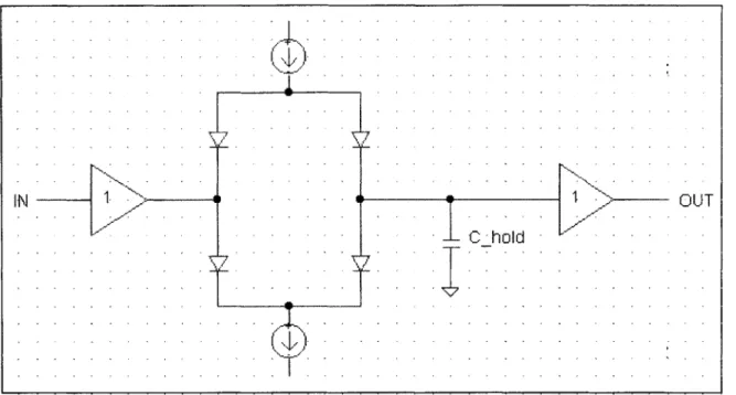
Figure 2.3 Typical sample-and-hold topology with 4-diode bridge analog switch.
The other additional block in a sub-ranging ADC is the second S/H circuit. In Chapter 2 it is argued that this input S/H amplifier must meet far stricter performance requirements than the second stage S/H. In order to understand the performance limitations of a S/H amplifier, a particular S/H architecture must be examined. A S/H consists of an input buffer, an analog switch, a capacitor on which the sampled voltage is held, and an output buffer. This thesis is concerned with high-speed A/D applications; therefore, a typical high-speed S/H topology is examined. Figure 2.3 shows a simple sample-and-hold topology with a high-speed analog switch topology, known as a diode bridge. The 4-diode bridge is the most suitable implementation of an analog switch in high-speed bipolar S/H applications. [10]
The operation of the 4-diode bridge is rather simple. While both of the current sources are conducting, all of the diodes are forward biased and the bridge is in sample mode. Any changes at the input to the bridge are tracked on the hold capacitor. In order to transition to hold mode, the current sources shut off and all of the diodes stop conducting current, effectively isolating the input to the bridge from the hold capacitor. In order to shut off the current sources, the voltage levels at the top and bottom of the bridge are often switched. This level change saturates the current sources and also reverse biases
Chapter 2 BACKGROUND
the diodes. The buffer amplifiers simply isolate the bridge from the input and output loads.
There are several sources of distortion in the S/H, and this distortion causes vital information about the sampled signal to be irretrievably lost. One such error is the hold pedestal introduced during the sample-to-hold transition. As mentioned earlier, when in track mode, all of the diodes are forward biased, and the diodes are then reversed biased to transition to hold mode. Associated with each of the diodes is some non-linear junction capacitance that stores charge. As these charges are expelled when the diodes are reverse-biased, any difference in the charge appears as a voltage perturbation on the hold capacitor. Since the charge expelled is dependent on the common-mode voltage on the hold capacitor, the pedestal varies nonlinearly with the input sample and causes distortion. This pedestal is a design parameter that can be controlled by appropriately choosing the size of the hold capacitor. [10]
The diodes also introduce error during the hold mode. Any real diode has some finite leakage current while reversed biased. This leakage charge is pulled off of the hold capacitor, and the result is a droop in the voltage on the hold capacitor during the hold mode period. Any input current to the second buffer amplifier is also drawn off of the hold capacitor and adds to the droop error. As with pedestal error, choosing a large hold capacitor can reduce droop error.
The current sources can also introduce distortion into the captured voltage. If the current sources are not matched, the diodes will be forward biased slightly differently. This introduces an error on the hold capacitor proportional to the incremental on resistance of the diode. A similar analysis shows that distortion is introduced if the two current sources do not turn off at exactly the same time. Both of these errors can be minimized
by clever current source design.
In addition to the various sources of distortion identified above, the held sample will be distorted with noise generated by each of the components surrounding the hold capacitor.
2.2 ADC Performance Limitations
There are several significant noise sources in the S/H shown in Figure 2.3. First, wideband thermal noise from the input buffer amplifier is integrated on the hold capacitor. Likewise, wideband thermal noise from the output buffer stage is directly added into the captured sample. Also, shot noise in the base current of the output amplifier integrates on the hold capacitor. Of course, this shot noise error would not exist in a CMOS buffer implementation because MOS devices do not have any gate current.
[10]
One final source of distortion is aperture jitter in the clock signal that causes the transition from sample mode to hold mode. This effect comes about because the clock transition does not occur at precisely equal time intervals. Instead, the sampling process can be characterized by an average time interval, T = 1 / fsamp, and a standard deviation of sampling instants around that average. This standard deviation is defined as the rms aperture jitter, Ta. If the input to the S/H amplifier is a Nyquist rate sinusoid (=n fsarn,/2),
with peak-to-peak amplitude VFS, the maximum error will occur at the zero crossing of the input [3]
V,, = nfSamPVFS (2.1)
2
If the rms aperture jitter is ips, a typical value for modern low jitter clocks, a lVpp, 500
MHz sinusoid will be sampled with a maximum rms voltage error of 1.6mV. This voltage error corresponds to a LSB error for an 8-bit converter. The aperture jitter effect must be averaged over a (typically sinusoidal) signal to obtain rms noise. When this is done, the general aperture-jitter-limited resolution of a S/H is found to be [11]
N log2 (2.2)
Having identified many sources of error in S/H amplifiers, D/A converters, and comparators, the issue becomes the identification of which error sources limit overall performance. In order to explore this issue, it is important to note that the majority of the distortion sources can be compensated for through circuit design techniques. For example, increasing the size of the hold capacitor can reduce leakage current errors in a
S/H, and consuming more power can speed up slow comparator settling. Solutions for 23
Chapter 2 BACKGROUND
aperture jitter errors are less obvious. The spectral purity of a clock is largely dependent on the crystal oscillator used to generate the clock signal. Given finite accuracy in the clock generation circuitry, it becomes a difficult task to develop circuit techniques to reduce clock jitter. As such, it is expected that clock jitter will determine the limit to which the performance of a given ADC can be pushed.
In support of this hypothesis, a survey of analog-to-digital converters, both commercial and experimental, is conducted in [3]. The analysis in this paper considers three dominant mechanisms through which A/D performance is limited: thermal noise, aperture jitter, and comparator metastability. Also, the performance metric focused on is the maximum resolution that can be achieved at a given sampling rate. The findings suggest that at sampling rates below 2MSPS, resolution is limited by thermal noise. For converters with sampling rates between 2MSPS and 4GSPS, resolution falls off by -1 bit for every doubling of the sampling rate. This behavior is attributed to errors from aperture jitter. Finally, for converters that operate above 4GSPS, comparator metastability limits performance. This thesis is focused on high-speed, high-resolution
A/D converters for the applications mentioned in Chapter 1, such as software radio. The
range of conversion speeds for such applications is between -100MSPS and -1GSPS. Therefore, [3] supports the hypothesis that aperture uncertainty is indeed the dominant performance-limiting factor.
25
Chapter 3
DELAY LINE ADC ARCHITECTURE
3.1
Architecture Overview
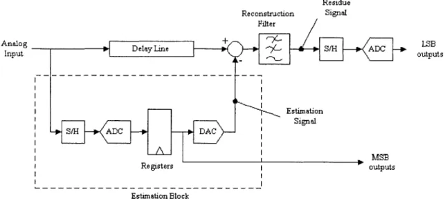
The proposed delay line ADC architecture is shown in Figure 3.1. The first stage consists of a delay line, a subtractor, and an estimation block, which is itself comprised of a coarse M-bit A/D converter, a set of digital registers and an estimation D/A converter. This is in contrast to the typical sub-ranging first stage, which does not contain the delay line or the registers but does contain a high-performance S/H block (see Chapter 2.1.2). The second stage of the delay line ADC is again similar to the second stage of the sub-ranging ADC, only it includes the low-pass reconstruction filter. As mentioned earlier, the goal of each of these changes is to reduce the demand on the S/H amplifiers in the sub-ranging configuration.
In a conventional sub-ranging architecture, the S/H block at the input to the first stage serves two purposes. First, it eliminates timing errors at the subtractor. As the signal propagates through the estimation block, some finite time delay will be introduced. Therefore, the correct estimate signal is not available to the subtractor for some finite propagation delay Tprop. The input S/H holds the sampled input value for some time Thold > Tprop. Therefore, at time Tprop after the input is sampled, the two signals that are input to
the subtractor correspond in the time domain.
The other purpose of the sub-ranging input S/H is to capture the time-varying input and holds while the estimation ADC performs the conversion. Without a S/H, the input signal to the first stage ADC might change before the comparators have completed their decision, and this results in a drop-off in the spurious-free dynamic range (SFDR). This
Chapter 3 DELAY LINE ADC ARCHITECTURE
Residue
Reconstruction Signal
Filter
Analog ___-eayEL' LSB
Input elay outputs
Estimation Signal S/H ADC - -- DAC T OR MSP Re gisters outputs Estimation Block
Figure 3.1 Proposed delay line ADC architecture.
effect can be dramatic, especially as input frequencies approach the Nyquist frequency. Therefore, a S/H preceding each A/D is necessary in high-speed converters. [12] Also, since this sampled value is propagated through to the second stage of the converter, it must be sampled to within the accuracy of the entire converter. It is important to note that an input S/H is not necessarily required for this purpose. In speed or low-resolution applications, the input signal may not change enough during the comparator decision time to cause an error. However, in high-speed applications, this is often not the case, and most high-speed ADCs have an input S/H. [12]
The delay line ADC architecture eliminates the need for this high-performance S/H block. It was just argued that one of the purposes of the sub-ranging input S/H block was to align the two signals at the input to the subtractor in the time domain. However, if the propagation delay through the estimation block Tprop, is well defined, this function can be replaced with a delay line. The delay through this delay network should also be Tprop for proper time alignment of signals. In the case of the delay line architecture, Tprop is in fact well defined. The propagation delay through the estimation ADC, or latency, is a dependent on the ADC architecture implemented. Also, the phase delay between the S/H clock and the register clock is a design parameter that can be varied. Finally, the delay
3.1 Architecture Overview 1.5 Time (seconds) 2 -8 x 10 0.25 0.2 -. . . . - - -. - - - .- - - - . -0.15 V- - - - - -0.1 I
--- - -
.-
-
.-
-
.-
-.
---
---
-
-
-..
.
-
-.
-.
-
-.
-------
.- - - - - ------ - - -- -- -- -- -- - - - - - - - ---- - - - ----- --- ---0.1 -0.15 -0.2 -0.25 1.5 Time (seconds)Figure 3.2 Delay line ADC waveforms. (a) Delayed input signal and estimation signal superimposed.
(b) Difference between the delayed input signal and the estimation signal, i.e. the unfiltered
residue signal.
through the DAC is determined by the switching and settling time of the DAC current sources. Therefore, the delay through this entire estimation block can be matched with a simple delay line, eliminating one of the needs for an input S/H block.
The other purpose of the input S/H in a sub-ranging architecture is to hold a steady input for the estimation ADC. However, this ADC is a coarse M-bit ADC (where M is typically 3-5 bits). Therefore, a high-performance S/H is not necessary. Instead, the capture function can be adequately performed by a S/H in the estimation path that samples the input with M-bit accuracy. Also, since this signal does not directly propagate into the second stage, an M-bit accurate S/H will not degrade performance. Therefore, the delay line A/D architecture eliminates the need for a high-performance sample-and-hold circuit in the first stage.
0.25 0.2 [ 0.151-0.1 0.05 0) 0r 0 0) cz -0.05 -0.1 -0.15 -0.2 -0.251 1 - - --- - - --
--
-
--
--
-- --
----
--..
..
. - - - -- - - --- ---. -. - -. -. . - - - -. . -.. 2 x 10 27 0.05 -o 0 C - 0) C-0.05 1Chapter 3 DELAY LINE ADC ARCHITECTURE
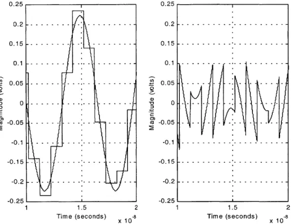
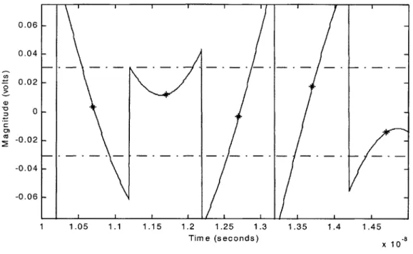
The low-pass reconstruction filter is added to the delay line A/D architecture to reduce the performance requirements of the second stage S/H block. In order to understand the performance requirements on the second stage S/H, the residue waveform must be examined. For this illustration, assume the input to the delay line ADC is a sinusoid. The output of the estimation block will be a quantized, zero-order hold version of that sinusoid. Figure 3.2a shows a 155MHz, 0.5Vp-p sinusoid, time shifted by the delay line, and the resulting estimation signal for an ideal (instantaneously DAC settling) 1GSPS, 4-bit estimation block. The estimate signal is then subtracted from the delayed input, leaving the residue signal that is shown in Figure 3.2b. In the absence of a reconstruction filter, this residue signal is converted by the second stage ADC.
The disadvantage of implementing the delay line ADC without a reconstruction filter can be seen in Figure 3.2b. The frequency content of the estimation signal contains the fundamental, or input, frequency, but it also contains many higher frequency harmonics. These harmonics are an artifact of the step-like response of a D/A converter. Therefore, the maximum rate of change of this residue signal is much greater than the maximum rate of change of the input signal. This increased rate of change places more strain on the second stage S/H. It must be able to sample an input that changes much faster than the fundamental with N-bit accuracy, where N is the number of bits resolved by the second stage.
The addition of the reconstruction filter reduces the maximum rate of change presented to the second stage ADC. In the frequency domain, the result of the reconstruction filter is an attenuation of the high frequency harmonics in the residue signal. The exact nature of this attenuation depends on the characteristics of the filter, which is a design parameter that will be explored in depth in Chapter 4. In the time domain, the effect of the reconstruction filter can be see in Figure 3.3, which shows the waveform from Figure
3.2b after filtering. In this example, the reconstruction filter is a fourth order lowpass
Butterworth filter with a 300 MHz comer frequency. Essentially, the unfiltered residue signal is smoothed out. In Figure 3.3, the maximum derivative of this smoothed residue signal is about 11 mV/ns. If the purpose of the estimation stage were to generate a 4-bit 28
3.1 Architecture Overview al) -0 Ca 0.25 0.2 0.15 0.1 0.05 0 -0.05 -0.1 -0.15 -0.2 -0.25 1 1.1 1.2 1.3 1.4 1.5 1.6 1.7 1.8 1.9 2 Time (seconds) x 10
Figure 3.3 Residue waveform convolved with 4 order Butterworth filter impulse response.
estimate, this smooth residue signal would be multiplied by a gain of 24 and then converted by the second stage. In this case, the maximum rate of change of the residue signal would be 176 mV/ns, which is significantly smaller than the maximum rate of change of the input signal, 245 mV/ns. Therefore, the reconstruction filter achieves its goal of reducing the rate of change of the residue signal to a level below the maximum input sinusoid slope.
-- -- - - - - - - - --- - - - - - --- --- - - - ---- --- - - - -- - - - --- --- --- --- - - -- - - - - - -- -- -- - - - -. -- - -- -. - -. -. - - - - -. - - - -. - - - - - - - - ---- - - - --. --. --. --. --.--. . . . . . . . 29
Chapter 3 DELAY LINE ADC ARCHITECTURE
3.2
Calibration
3.2.1 Reconstruction Filter Issues
In the previous section, the benefits of the reconstruction filter were explained. The drawback of the reconstruction filter is the introduction of an effective error into the residue signal. In order to analyze this error, consider the residue signal without the reconstruction filter, shown in Figure 3.2b. The peak-to-peak magnitude of this signal is on the order of 200 mV. However, the accuracy of the estimation ADC is 4 bits in this example, and the estimation DAC is assumed to be at least as accurate as the estimation
ADC. Therefore, at the sampling instants (0, Ins, 2ns...), the value of the unfiltered
residue signal is within about +/- LSB, or 64mV peak-to-peak in the example shown.
This limit on the unfiltered residue error at the sampling instants is illustrated in Figure 3.4. This plot is simply a repeat of Figure 3.2b, zoomed in around several sampling instants. The horizontal lines delineate the +/- LSB band in which the waveform must lie at the sampling instants. In the particular example shown, the sampling instants are at 10.2ns, 11.2ns, 12.2ns, and so on. The value of the unfiltered residue waveform at these time instants is marked with stars. As shown, the unfiltered residue signal always lies within this error band at the sampling instants.
However, the filtering operation smears the residue signal in the time domain. Once filtered, the magnitude of the residue signal at the sampling instants is no longer guaranteed by the accuracy of the estimation block. In Figure 3.3, the magnitude of the filtered residue signal, about 30 mVp-p, is smaller than the 4-bit accuracy +/- 1/2 LSB limit.
If, however, the magnitude of the filtered residue signal were not within the +/- LSB error band, the accuracy of the delay line converter would be limited by the size of the residue signal. Non-optimal design values, such as a low oversampling ratio or high filter passband edge frequencies, cause the residue signal magnitude to increase and introduce
3.2 Calibration
error into the residue signal. Tradeoffs involved in these design choices are discussed in Chapter 4.
An interesting effect of the estimation operation can be extracted from Figure 3.5. In this figure, the simulation is identical to the simulation shown in Figure 3.2b, except that the input signal is a higher frequency sinusoid at 250MHz. Note that the period of the filter residue waveform is 4ns, which is the same as the period of the 250MHz input. The filtered residue is in phase with the delayed input, and this suggests that the magnitude of the fundamental component of the estimation signal is smaller than the delayed input. This effect is caused by the zero order hold function of the estimation block. The Fourier transform of a zero order hold is a sinc function, and the gain of this transform is not constant in the passband. Therefore, the magnitude of the estimate signal fundamental component is smaller than the delayed input signal. The zero-order-hold-induced error could be removed with a filter that has impulse response [13]
jo>T /2
H
(j(O)=
e (3.1)2sin(oT / 2) (0)
Such a filter cannot be exactly realized in practice, and would a filter that approximates this impulse response would have to be implemented. This inverse-sinc filter is not implemented in this thesis, it is merely suggested as a possible optimization.
Chapter 3 DELAY LINE ADC ARCHITECTURE
1.05 1.1 1.15 1.2 1.25 1.3
Time (seconds)
Figure 3.4 Unfiltered residue waveform, zoomed in around 5
identical to waveform shown in Figure 3.2b.
x 10
sampling instants. Simulation set up is
1 1.2 1.4 1.6 1.8 2 2.2
Time (seconds)
2.4 2.6 2.8
-8
X 10
Figure 3.5 Residue waveform with reconstruction filter included in delay line ADC. Input frequency is 255MHz and the estimation block oversamples by a factor of 2. Reconstruction filter is a 4h order Butterworth with a 300MHz passband edge.
32 0 Z) 0.06 0.04 0.02 0 -0.02 -0.04 -0.06 I I I I I I I -I I I 0 0) co 2 0.2 0.15 0.1 0.05 0 -0.05 -0.1 -0.15 -0.2 -0.25 . I . r . .
-- -
---
--
---
---
-- - -
--
-
-.
-. .--
.-
...-
-
.
--- --- --- - -- - - -- --- -- - - --- --- --- --- --- --- --- --- --- --- --- --- --- --- --- --- --- - - - - - - -- --- - - - - -- - - -.- .- .- --.. .- -. --. --. --.-I
I
I
1 1.35 1.4 1.453.2 Calibration
3.2.2 Necessity of Calibration
Due to the smearing function of the reconstruction filter, the residue waveform that is converted by the second stage is not directly related to the output of the estimation DAC. Instead, the residue waveform is the convolution of the filter impulse response and the unfiltered residue signal, which is in turn the difference between the delayed input and the output of the estimation DAC. Therefore, the output of the second stage ADC, i.e. the digitized residue signal, cannot be directly combined with the digital signal from the estimation block in order to get an high resolution representation of the input signal. Instead, the correct digital value can be obtained by combining the output of the second stage ADC should with the result of the estimation signal convolved with the filter response.
In order to facilitate this calculation, the filter needs to be calibrated. If the filter impulse response were known, any estimation signal could be convolved with this known response in order to find the portion of the residue signal that is due to the estimate.
Instead of simply calibrating the filter, however, both the estimation DAC and the reconstruction filter can be calibrated simultaneously. While DAC calibration is not necessary, the calibration algorithm described in the next section requires little more effort than filter calibration alone. Also, calibrating the DAC should eliminate sources of error in the DAC current switches from affecting system performance.
The following section describes the calibration algorithm necessary for filter calibration and also briefly discusses the advantages it offers. Tradeoffs involved in the calibration process are described in more detail in Chapter 4.
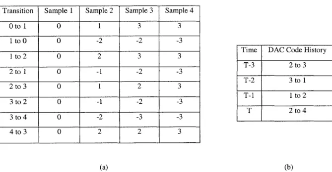
3.2.3 Calibration Algorithm
To calibrate the response of the estimation DAC and filter, the step response of each bit level transition, e.g. '0001' to '0010' or '1101' to '1100', is measured. The digital code
Chapter 3 DELAY LINE ADC ARCHITECTURE
at the input to the estimation DAC is switched while there is no input signal to the delay line, and the resulting digital output codes from the second stage are stored. Given an M-bit estimation stage and an N-M-bit second stage, there are 2*2m transitions calibrated, and each calibration is known to N-bit accuracy. The number of samples that must be taken for each transition depends on the settling time of the DAC and filter. Each transition is sampled until the response settles to within N-bit accuracy.
Once all of the step responses are known, the filter output for any given DAC code can be digitally reconstructed. To reconstruct this signal, each of the previous X DAC codes in a history table, where X is the number of sample periods needed for the filter output to settle to N-bit accuracy, are combined with data stored during the calibration process to add up, step by step, the filtered estimation signal.
During normal operation of the delay line ADC, the digital output of the estimation ADC is used to reconstruct the component of the filter output that is due to the estimation signal. By summing this digitally reconstructed signal with the output of the second stage, a digital representation of the input signal, after being delayed and filtered, is determined. It is assumed that the passband of the low-pass filter contains all frequencies up to the Nyquist frequency, so the filtering operation should not affect the input signal and this calculated digital representation of the input signal should be accurate.
In order to illustrate the calibration scheme, a simple example is now explored. Consider a 2-bit estimation stage and a 3-bit second stage. Figure 3.6 shows both the calibration data table and the digital estimation code history table. As shown in the calibration data table, it takes four samples for the filter to settle to within 3-bit accuracy.