HAL Id: hal-01911994
https://hal.archives-ouvertes.fr/hal-01911994
Submitted on 5 Nov 2018
HAL is a multi-disciplinary open access
archive for the deposit and dissemination of
sci-entific research documents, whether they are
pub-lished or not. The documents may come from
teaching and research institutions in France or
abroad, or from public or private research centers.
L’archive ouverte pluridisciplinaire HAL, est
destinée au dépôt et à la diffusion de documents
scientifiques de niveau recherche, publiés ou non,
émanant des établissements d’enseignement et de
recherche français ou étrangers, des laboratoires
publics ou privés.
Fast and inexpensive method for the fabrication of
transparent pressure-resistant microfluidic chips
Alexandre Martin, Sébastien Teychené, Séverine Camy, Joelle Aubin
To cite this version:
Alexandre Martin, Sébastien Teychené, Séverine Camy, Joelle Aubin. Fast and inexpensive method
for the fabrication of transparent pressure-resistant microfluidic chips. Microfluidics and Nanofluidics,
Springer Verlag, 2016, 20 (6), pp.1-9. �10.1007/s10404-016-1757-7�. �hal-01911994�
O
pen
A
rchive
T
oulouse
A
rchive
O
uverte
(OATAO)
OATAO is an open access repository that collects the work of some Toulouse
researchers and makes it freely available over the web where possible.
This is an author’s version published in:
http://oatao.univ-toulouse.fr/
20534
To cite this version:
Martin, Alexandre and Teychené, Sébastien and Camy, Séverine and Aubin, Joelle Fast
and inexpensive method for the fabrication of transparent pressure-resistant
microfluidic chips. (2016) Microfluidics and Nanofluidics, 20 (6). ISSN 1613-4982
Any correspondance concerning this service should be sent to the repository administrator:
[email protected]
Fast and inexpensive method for the fabrication of transparent
pressure-resistant microfluidic chips
Alexandre Martin1 · Sébastien Teychené1 · Séverine Camy1 · Joëlle Aubin1
1 Introduction
Pressure-resistant microfluidic chips have become of increas-ing interest in recent years for flow chemistry (Benito-Lopez et al. 2008; Verboom 2009; Razzaq et al. 2009; Trachsel et al.
2008), processes involving supercritical fluids (Benito-Lopez et al. 2007; Marre et al. 2012; Luther and Braeuer 2012), materials science (Marre et al. 2012) and also as analysis tools (Benito-Lopez et al. 2005; Keybl and Jensen 2011; Dorobantu Bodoc et al. 2012; Pinho et al. 2014; Macedo Por-tela da Silva et al. 2014; Gothsch et al. 2015; Blanch-Ojea et al. 2012; Zhao et al. 2013; Ogden et al. 2014). Indeed, it is well known that operating processes at high pressure modify fluid properties, which may enable enhanced kinetics, con-version and selectivity (Verboom 2009; Benito Lopez et al.
2007; Kobayashi et al. 2005). In addition to this, miniaturi-zation of these chemical systems further enhances mass and heat transfer and provides improved control of in situ condi-tions and process safety, which is particularly important for high-pressure processes (Hessel et al. 2004).
With the emergence of high-pressure applications in microfluidics, the development of highly resistant micro-fluidic chips has been the focus of a number of studies. Among these, glass/glass (Tiggelaar et al. 2007) and sili-con/glass microreactors (Trachsel et al. 2008; Murphy et al. 2007; Marre et al. 2010) have shown to resist pres-sures of up to 400 bar. The microchannels are constructed using either wet or dry etching methods and then are sealed to glass via anodic bonding. These microchips have the advantage of resisting high pressures and also allow optical access to the flow for in situ characterization. In addition, silicon/glass chips have the asset of enabling very good temperature control due to the high thermal conductivity of the silicon wafer (Marre et al. 2010). However, the fab-rication methods employed require clean room facilities,
Abstract The recent rise of high-pressure applications in
microfluidics has led to the development of different types of pressure-resistant microfluidic chips. For the most part, however, the fabrication methods require clean room facili-ties, as well as specific equipment and expertise. Further-more, the resulting microfluidic chips are not always well suited to flow visualization and optical measurements. Herein, we present a method that allows rapid and inexpen-sive prototyping of optically transparent microfluidic chips that resist pressures of at least 200 bar. The fabrication method is based on UV-curable off-stoichiometry thiol-ene epoxy (OSTE+) polymer, which is chemically bonded to glass. The reliability of the device was verified by pressure tests using CO2, showing resistance without failure up to at least 200 bar at ambient temperature. The microchips also resisted operation at high pressure for several hours at a temperature of 40 °C. These results show that the poly-mer structure and the chemical bond with the glass are not affected by high-pressure CO2. Opportunities for flow vis-ualization are illustrated by high-pressure two-phase flow shadowgraphy experiments. These microfluidic chips are of specific interest for use with supercritical CO2 and for optical characterization of phase transitions and multiphase flow under near-critical and critical CO2 conditions.
Keywords Microchip · Fabrication · High pressure ·
Supercritical CO2 · Visualization
* Joëlle Aubin
1
Laboratoire de Génie Chimique, CNRS, INPT, UPS, University of Toulouse, 4 Allée Emile Monso, BP-84234, 31030 Toulouse, France
specific equipment and expertise, and entail relatively high operating and fabrication costs, which are limiting when rapid prototyping is required. Furthermore, silicon/glass chips may be limited for some optical measurement tech-niques due to the opaque and reflective nature of the silicon wafer.
Some simpler glass devices based on fused silica capil-laries have also been proposed for high-pressure applica-tions (Macedo Portela da Silva et al. 2014; Marre et al.
2009). Marre et al. (2009) showed the use of silica cap-illaries under pressure conditions ranging from 80 to 180 bar. Macedo Portela da Silva et al. (2014) demon-strated that operating pressures up to 300 bar could be achieved by embedding silicon capillaries in epoxy resin. Both of these studies also showed that two-phase flow can be easily visualized and characterized by shadowgraphy in such capillaries. However, more elaborate optical charac-terization techniques, such as micro particle image veloci-metry, would be limited in these devices because of prob-lems related to optical distortion, poor light transmission and focal depth.
Rapid prototyping methods based on polymer molding and milling are very popular in the academic microfluid-ics community because they are inexpensive, fast and easy to implement. They also allow the fabrication of planar geometries in transparent materials, which facilitate the use of optical visualization and measurement techniques. Polydimethylsiloxane (PDMS) is the most widely used polymer for such applications; however, its low Young’s modulus means that it is very elastic and as a result, the microchannels are deformed under pressure or high-flow rates. It has also poor solvent compatibility so appli-cations are limited. Recently Sollier et al. (2011) have analyzed the performance of other rapid prototyping poly-mers, including thermoset polyester (TPE), polyurethane methacrylate (PUMA) and Norland Adhesive 81 (NOA81), for high-pressure injections. They showed that PUMA and NOA81 chips resisted pressures up to approximately 8 bar and 5 bar, respectively, before leakage or delamination. The maximum pressure resistance of their setup made of NOA81 is considerably lower than the 15 bar reported by Bartolo et al. (2008). The TPE chips, on the other hand, resisted the maximum pressure tested of approximately 10 bar without any mechanical failure. TPE, PUMA and NOA81 were also shown to have optical transmission simi-lar to glass and have good solvent compatibility compared with PDMS.
Recently, Carlborg et al. (2011) have developed a rapid prototyping method based on off-stoichiometry thiol-enes (OSTEs), which allow excellent adhesion to silicon, glass, many metals or even another layer of this polymer, due to covalent bonds and offer very good optical transmission. It also allows surface modifications, tunable mechanical
properties and reliable sealing with other substrates, and the authors have since demonstrated a number of custom specificities (Sandström et al. 2015; Saharil et al. 2012; Haraldsson et al. 2014). OSTE has also shown compatibil-ity with solvents such as toluene, water, acetone, ethanol, methanol and dimethyl sulfoxide (www.ostemers.com). However, up until now, pressure resistance has not been the objective of their studies and the chips have only been shown to resist pressures in the range of 4–7 bar (Sand-ström et al. 2015; Saharil et al. 2013).
In this article, a new method for the fabrication of microchannels made of UV-curable OSTE (OSTEMER Crystal Clear) and glass, compatible with possible utiliza-tion with supercritical carbon dioxide, is presented. The pressure resistance of the microfluidic chips is demon-strated by flowing CO2 at high pressure through the micro-channel. The method enables inexpensive rapid prototyping without the requirement of any highly specific microfab-rication equipment. The resulting microfluidic chips have the advantage of being optically transparent and planar, thereby being well suited to visualization via shadowgra-phy, and particularly to laser-based methods like micro particle image velocimetry and optical measurement tech-niques based on light transmission or reflection, such as spectrophotometry (UV–Vis, IR), that benefit from pla-nar surfaces. Indeed, this fabrication method provides the possibility to perform multiphase flow visualization stud-ies in microchannels—that have been largely investigated at ambient pressures (e.g., Garstecki et al. 2006; Gupta and Kumar 2010; Abadie et al. 2012; Zaloha et al. 2012; King et al. 2007; Wang et al. 2015)—under high-pressure conditions.
2 Experimental
2.1 Microchannel geometry
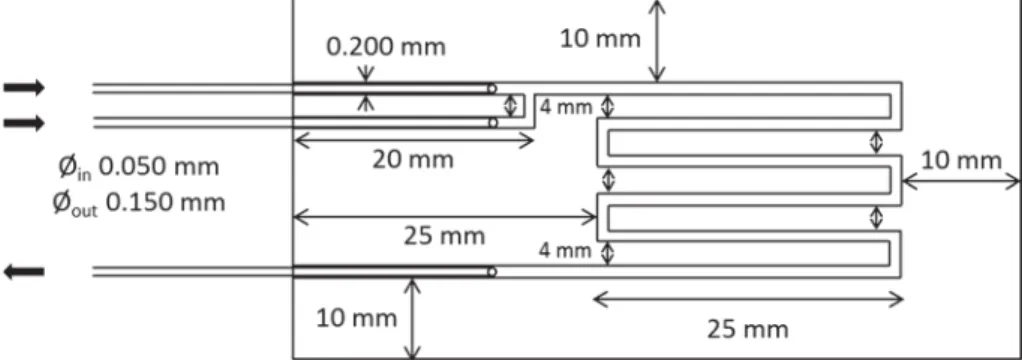
The microchannel fabricated in this study is a 200 µm square cross-sectional channel with a meandering topology that has a total length of 12.5 cm as shown in Fig. 1. The two inlets are connected by a T-junction inside the micro-chip structure.
2.2 Fabrication method of microchannels and assembly of chips
The microfluidics chips are fabricated with a soft lithogra-phy method, which uses OSTEMER Crystal Clear. OSTE-MER Crystal Clear is a polymer used for quickly building optically transparent, hard and robust microstructures using inexpensive laboratory equipment. This polymer is based on the off-stoichiometry thiol-ene-epoxies and features a
two-step curing process. It is initially shaped using UV-casting and is then hardened and bonded to itself—or other materials—via a second thermal cure. The first cure geo-metrically defines the polymer into a micropatterned inter-mediate stage, but a predetermined amount of epoxy groups remain unreacted. In a second curing step, all the remaining epoxy groups are reacted to form an inert polymer, which stiffens and bonds covalently to most other surfaces that it is in contact with, similarly to epoxy glues.
The fabrication method presented here is based on that previously published by Carlborg et al. (2011) and has been modified in order to create microfluidic chips that allow high-pressure operation. The fabrication method is com-prised of several steps, as shown in Fig. 2.
The principal differences with this new method, com-pared with the original method provided by Carlborg et al. (2011), are:
• The use of a 2-mm-thick glass slide as a base to which all of the other chip layers are strongly bonded;
• The use of a thin (and hence slightly flexible) silanized cover slip to seal the microchannel. This ensures very good contact between the surfaces and improved bond-ing strength.
• The reinforcement of the sealed microchannel with an additional layer of OSTEMER and a final 2-mm glass slide which also provides a planar top surface for pos-sible optical measurements.
The specific details of the fabrication procedure are pro-vided below in Fig. 2. Note that since some of the materials used in this protocol (i.e., photoresist dry films and OSTE-MER Crystal Clear) are UV sensitive, the microchip fabri-cation was carried out in a UV-protected room.
Dry film fabrication (steps 1–4) Two 100-µm lay-ers of a dry film photoresist (WBR2100 DuPont, France) are laminated one-by-one on a glass slide using a heated roll laminator (MEGA Electronics). The glass slide with the dry film is then heated for 20 min at 60 °C. The mul-tilevel dry film is then exposed to UV LED light through
Fig. 1 Schematic diagram with dimensions of the microchan-nels fabricated in this study. ∅in
and ∅out denote the diameters of
the inlet and outlet capillaries, respectively
Fig. 2 Schematic overview of microchannel fabrication. 1–4 Dry film mold fabrication. 5–6 PDMS mold fabrication. 7–10 Molding of OSTEMER and sealing of the microchannel
a photolithography mask using a UV-KUB 2 exposure masking system (Kloe, France) for 19 s at 25 mW/cm2 to obtain the desired channel topology. This time is sufficient to cure the thickness of the dry film without degrading it due to over exposure. Following this, the glass slide is put on a heated plate for 60 s at 100 °C. The dry film mold is developed using a potassium carbonate solution (1 % w/w), which is applied continuously using a spin coater (SPS Spin 150) for 6 min at 900 rpm. The mold is then rinsed with distilled water using the same spin coating pro-cedure as for the developer. The mold is thoroughly dried with compressed air and baked for 60 s on heated plate at 100 °C. The mold is then dipped in a bath of toluene for 1 min. This helps in removing the PDMS mold in the next step. The glass slide with the dry film is then left for 12 h in a warm oven (65 °C) to remove all toluene residuals.
Fabrication of the PDMS mold (steps 5–6) Sylgard 184 silicone elastomer kit (Dow Corning, USA) is used to pre-pare a mixture of PDMS and curing agent with a 10:1 ratio. The mixture is degassed in a desiccator and then poured over the dry film mold, which is degassed again. The PDMS is then cured for 12 h at 65 °C. The PDMS mold is peeled off the dry film mold, resulting in a negative micro-channel structure printed on the PDMS (step 6).
Molding and curing of the OSTEMER Crystal Clear (step 7) 3 g of degassed liquid OSTEMER Crystal Clear are placed on a 2-mm-thick (60 mm × 38 mm) glass side. The PDMS mold is degassed and immediately placed over the top of the liquid OSTEMER for 15 min so that any bub-bles trapped between the OSTEMER liquid and the PDMS mold have time to be absorbed into the PDMS structure. The ensemble is then exposed to UV light for 35 s at 25 mW/cm2 using the UV-KUB 2 masking system in order to partially cure the OSTEMER before the sealing step. The PDMS mold is then cautiously peeled off the OSTE-MER layer.
Sealing the chip (steps 8–10) Before sealing the micro-channel, fused silica capillaries (ID 50 µm, OD 150 µm, C.I.L. TSP050150M010) are cautiously inserted at the inlet and outlet of the microchannel. Here, capillary con-nections are preferred to nanoports or modular connec-tions (e.g., those used in Marre et al. 2010) due to better resistance under high-pressure flows. A glass cover slip (Menzel-Gläser #1, 0.13–0.16 mm-thick), which has previously been silanized in a mercapto silane solution [(3-Mercaptopropyl)-trimethoxysilane in ethanol 2 % w/w] for 15 min, blown with nitrogen and dried for 30 min in a 100 °C oven, is then positioned over the OSTEMER polymer layer to cover the channel. The silanization of the cover slip enables better bonding of OSTEMER epoxies groups to glass surface. Rubbing a flat blade over the top of the cover slip ensures good contact between the cover
slip and the OSTEMER without trapping any air bubbles, which could weaken the bonding. Note that a thin cover slip is preferred over a 1- or 2-mm glass slide since it is slightly more flexible and therefore improves the contact between the surfaces and hence the adherence. Tests were carried out using 1- and 2-mm glass slides to directly seal the channels, but due to the rigidity of the glass slides, the bonding was poor, resulting in leakages at moderate pres-sures (around 30 bar). Two grams of uncured liquid OSTE-MER are then poured over the cover slip, and a 2-mm glass slide is placed on top. The chip is then exposed to UV light for 35 s at 25 mW/cm2, followed by a heating for 12 h at 85 °C to complete the reticulation process of the OSTE-MER and to ensure that it is strongly bonded to the glass. The purpose of this second OSTEMER layer and the final glass slide is to reinforce the glass cover slip and increase the pressure resistance of the microfluidic chip while keep-ing a planar top surface for possible optical measurements. It also ensures that the capillaries are kept securely in place within the square cross-sectional microchannel and that no leaks occur. The microfluidic chip resulting from this fabri-cation process is presented in Fig. 3.
2.3 Visualization of the chip structure
To verify the different layers of the chip, the cross sec-tion was examined using an optical microscope fitted with a digital camera (Nikon ECLIPSE MA 200). A sample was cut from the chip and then embedded in epoxy resin, which acts as a support. The resin was then finely polished using silicon carbide abrasive paper (P4000 grit). Figure 4
illustrates a transverse slice of a chip showing the differ-ent layers and a 200 × 200 µm microchannel cross sec-tion. The lower layer is the 2-mm glass support. Just above is the OSTEMER layer in which the cross section of the microchannel can be seen. The microchannel dimensions have been correctly reproduced from the PDMS mold, and the sides of channel appear very straight. Above the
OSTEMER layer is the glass cover slip. The irregular edges of the glass support and cover slip are only due to cutting and polishing of the sample that is required for observing the cross section. The bonded surfaces of the OSTEMER polymer with both the glass slide and the cover slip are very satisfactory without imperfections.
Measurement of effective channel size reveals a maxi-mum difference of 10 % on each dimension of the channel. The precise replication of the channel shape from the mold depends on the development time of the dry film mold and the duration that the OSTEMER is exposed to UV. The durations provided in the description of the fabrication method have been previously optimized by trial and error. Note that it may be necessary to adapt the duration of some steps if other channel dimensions are desired.
2.4 Pressure tests
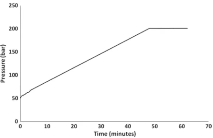
Before evaluating the pressure resistance of the OSTEMER chips, preliminary tests were conducted to verify that the microchannel was not blocked and enabled the circulation of CO2 at atmospheric pressure. The pressure resistance of the microchips was then evaluated by applying a con-stant pressure gradient of 3 bar/min by means of a high-pressure syringe pump (Teledyne ISCO, model 260D). The objective was to determine the pressure at which burst-ing, breakage or any other default of the microchip was observed. Tests were limited to 200 bar to avoid damag-ing part of the experimental system and flow circuit. Three microchips were tested and gave identical results. Figure 5
shows an example graph of the pressure applied to one of the microchips. As shown, there is a constant increase of the measured pressure until the maximum applied pressure of 200 bar without rupture of the glass or delamination of the different glass and polymer layers within the chip. Once at 200 bar, the tested channels were maintained at this pres-sure for approximately 20 min.
To further test the resistance and reliability of the microchip under high-pressure conditions, the pressure resistance of long operating periods was also verified. The microchannel was fed with CO2 at constant pressure by means of the same high-pressure pump by applying a constant fluid pressure in the chip and then by increasing the pressure with 10 bar steps at regular intervals. The time evolution of pressure at the inlet of the microchannel is recorded. Pressure step experiments were carried out using three different microchips, and the results are shown in Fig. 6. Initially, the chips were fed with CO2 at 50 bar; the
pressure was then increased by 10 bar every 45−60 min for a total operating time of more than 6 h. After an hour at 100 bar, the pressure was slowly decreased down to atmos-pheric pressure.
From the results in Fig. 6, it can be seen that these microchips also resist long operating times at high pressure without any signs of failure.
Fig. 4 Zoom on the cross section of the chip clearly showing the
dif-ferent layers around the 200 × 200 µm channel Fig. 5 Constant gradient pressure test of the OSTEMER/glass
micro-chip. A pressure of 200 bar is achieved without rupture or leakage
Fig. 6 Pressure tests of three different OSTEMER–glass microchips. Microchips were fed with CO2 at 50 bar, which was increased by
2.5 Flow visualization tests
In order to demonstrate the effectiveness of the hybrid OSTEMER–glass microchips, flow visualization tests were performed by shadowgraphy. To do this, an experimental rig was set up as follows. Fluid is pumped into the micro-channel using high-pressure pumps (Teledyne ISCO, mod-els 260D and 100 DX for CO2 and ethanol respectively). To maintain the pressure in the microchannel, a 250-mL tank is used as back-pressure buffer at the outlet of the microchannel. A mass flow controller (mini CORI-FLOW ML120 Bronkhorst) was used to regulate the pump motion to maintain a constant mass flow rate at the inlet of the microchip. The flow rate of ethanol was maintained directly by the pump setting. Fluids can be preheated before the entrance of microchip using a heated bath, and the LED panel (PHLOX White led Backlight 200 × 200) on which the microchip is placed for flow visualization enables the system to be maintained at a constant temperature of 40 °C. A high-speed CCD camera (Mikrotron EoSens CL 1.3 Megapixels) is used to take image flow sequences at 500 frames per second. Examples of two-phase flow images are provided in Figs. 7 and 8.
Figure 7 shows gas–liquid CO2 flow during the
transi-tion from the liquid state to the gas state at 22 °C (ambi-ent temperature) and 60 bar (which is indeed the vapor pressure of CO2 at 22 °C). CO2 Taylor bubbles that have been formed within the liquid CO2 flow are clearly visible.
This shows the potential of these microchips to be used to observe phase transitions of pure fluids or mixtures.
Figure 8 shows the formation of CO2 bubbles in ethanol (EtOH) at 60 bar and 40 °C. A constant EtOH flow rate of 50 µL/min was fed to the main (top horizontal) channel, and the CO2 gas at 100 µL/min was pinched off from the inlet at the T-junction. In this experiment, both fluids are heated by passing through a heated bath before the entrance of the chip and maintained at temperature by the LED panel used
for shadowgraphy. The Taylor bubbles are clearly visible in the EtOH, and the images are of the same quality as those obtained in our previous works using silicon wafer and glass channels (Abadie et al. 2012; Zaloha et al. 2012). This demonstrates the potential of these microchips to be used to study the fundamentals of bubble formation at high pressure.
2.6 Time and cost of the fabrication process
The dry film and PDMS molds are reusable and can be made in less than 2 h each, with an additional 12 h of drying time. These molds can be used several times to make the OSTE-MER microchannels, and by employing several PDMS molds, a number of microfluidic chips can be made in parallel.
After investment of the UV light source and the heated laminator, and not including labor, the cost required to fabricate one microfluidic chip following the method described in this paper is less than 20 euros. This corre-sponds to 5 grams of OSTEMER Crystal Clear, two 2-mm glass slides, one cover slip, 30 cm of fused silica capillar-ies for the inlets and outlet, as well as the fabrication cost of the reusable dry film and PDMS molds. This cost is ten times less than the inexpensive devices proposed by Mac-edo Portela da Silva et al. (2014) and is a much more acces-sible solution than buying commercial microfluidic chips that may cost several hundreds of euros.
3 Conclusion
A fast and inexpensive method for the fabrication of trans-parent pressure-resistant microchannels has been presented. The fabrication method is based on soft lithography using an optically transparent polymer called OSTEMER Crystal Clear. Once the molds are prepared, the microfluidic chips can be prepared in less than 2 h with 12 h drying time for less than 20 euros per chip. Moreover, neither clean room facilities nor specific fabrication equipment (apart from a laminator and a UV radiation source) are required. The microfluidic chips have been shown to resist high pressures for several hours and for pressures at least up to 200 bar.
These entirely transparent pressure-resistant microflu-idic chips offer the possibility to observe and measure flow characteristics and transport phenomena in complex mul-tiphase flows operating at high pressure, e.g., supercritical CO2 and liquid or ionic liquid dispersions. The planar and optically transparent nature of the microfluidic chips also enables distortion-free visualization without reflection, and they are therefore better adapted to measurement tech-niques, such as high-speed imaging, micro particle veloci-metry, laser-induced fluorescence and spectrophotometry (UV–Vis, IR), compared with glass capillaries or silicon wafer chips.
Fig. 7 Shadowgraph of CO2 gas bubbles forming in liquid CO2
at the saturation vapor pressure (60 bar at 22 °C) as the pressure is decreased
Fig. 8 Shadowgraph of CO2 Taylor bubbles formation in EtOH at
60 bar and 40 °C. EtOH flow rate is 50 µL/min and gas flow rate is 100 µL/min
Acknowledgments The authors would like to thank Tommy Haralds-son and Un Weiyang from Mercene Lab for providing materials and advice on the fabrication process. They would also like to thank L. Prat from The University of Toulouse for valuable discussions.
References
Abadie T, Aubin J, Legendre D, Xuereb C (2012) Hydrodynamics of gas–liquid Taylor flow in rectangular microchannels. Microfluid. Nanofluidics 12:355–369. doi:10.1007/s10404-011-0880-8
Bartolo D, Degré G, Nghe P, Studer V (2008) Microfluidic stickers. Lab Chip 8:274–279
Benito-Lopez F, Verboom W, Kakuta M, Gardeniers JGE, Egberink RJM, Oosterbroek ER, van den Berg A, Reinhoudt DN (2005) Optical fiber-based on-line UV/Vis spectroscopic monitoring of chemical reaction kinetics under high pressure in a capillary microreactor. Chem Commun. doi:10.1039/b500429b
Benito-Lopez F, Tiggelaar RM, Salbut K, Huskens J, Egberink RJM, Reinhoudt DN, Gardeniers HJGE, Verboom W (2007) Substan-tial rate enhancements of the esterification reaction of phthalic anhydride with methanol at high pressure and using supercritical CO2 as a co-solvent in a glass microreactor. Lab Chip 7:1345.
doi:10.1039/b703394j
Benito-López F, Egberink RJM, Reinhoudt DN, Verboom W (2008) High pressure in organic chemistry on the way to min-iaturization. Tetrahedron 64:10023–10040. doi:10.1016/j. tet.2008.07.108
Blanch-Ojea R, Tiggelaar RM, Pallares J, Grau FX, Gardeniers JGE (2012) Flow of CO2–ethanol and of CO2–methanol in a
non-adiabatic microfluidic T-junction at high pressures. Microfluid. Nanofluidics 12:927–940. doi:10.1007/s10404-011-0927-x
Carlborg CF, Haraldsson T, Öberg K, Malkoch M, van der Wijngaart W (2011) Beyond PDMS: off-stoichiometry thiol–ene (OSTE) based soft lithography for rapid prototyping of microfluidic devices. Lab Chip 11:3136. doi:10.1039/c1lc20388f
Dorobantu Bodoc M, Prat L, Xuereb C, Gourdon C, Lasuye T (2012) Online monitoring of vinyl chloride polymerization in a micro-reactor using Raman spectroscopy. Chem Eng Technol 35:705– 712. doi:10.1002/ceat.201100564
Garstecki P, Fuerstman MJ, Stone HA, Whitesides GM (2006) Formation of droplets and bubbles in a microfluidic T-junc-tion—scaling and mechanism of break-up. Lab Chip 6:437. doi:10.1039/b510841a
Gothsch T, Schilcher C, Richter C, Beinert S, Dietzel A, Büttgenbach S, Kwade A (2015) High-pressure microfluidic systems (HPMS): flow and cavitation measurements in supported silicon microsys-tems. Microfluid. Nanofluidics 18:121–130. doi:10.1007/ s10404-014-1419-6
Gupta A, Kumar R (2010) Effect of geometry on droplet formation in the squeezing regime in a microfluidic T-junction. Microfluid. Nanofluidics 8:799–812. doi:10.1007/s10404-009-0513-7
Haraldsson T, Carlborg CF, van der Wijngaart W (2014) OSTE: a novel polymer system developed for Lab-on-Chip. In: SPIE MOEMS-MEMS. International society for optics and photonics, pp 897608–897608
Hessel V, Hardt S, Löwe H (2004) Chemical micro process engi-neering: fundamentals, modelling and reactions. Wiley-VCH, Weinheim
Keybl J, Jensen KF (2011) Microreactor system for high-pressure continuous flow homogeneous catalysis measurements. Ind Eng Chem Res 50:11013–11022. doi:10.1021/ie200936b
King C, Walsh E, Grimes R (2007) PIV measurements of flow within plugs in a microchannel. Microfluid. Nanofluidics 3:463–472. doi:10.1007/s10404-006-0139-y
Kobayashi J, Mori Y, Kobayashi S (2005) Hydrogenation reactions using scCO2 as a solvent in microchannel reactors. Chem Com-mun. doi:10.1039/b501169h
Luther SK, Braeuer A (2012) High-pressure microfluidics for the investigation into multi-phase systems using the supercritical fluid extraction of emulsions (SFEE). J Supercrit Fluids 65:78– 86. doi:10.1016/j.supflu.2012.02.029
Macedo Portela da Silva N, Letourneau J-J, Espitalier F, Prat L (2014) Transparent and inexpensive microfluidic device for two-phase flow systems with high-pressure performance. Chem Eng Tech-nol 37:1929–1937. doi:10.1002/ceat.201400028
Marre S, Aymonier C, Subra P, Mignard E (2009) Dripping to jetting transitions observed from supercritical fluid in liquid microco-flows. Appl Phys Lett 95:134105. doi:10.1063/1.3242375
Marre S, Adamo A, Basak S, Aymonier C, Jensen KF (2010) Design and packaging of microreactors for high pressure and high tem-perature applications. Ind Eng Chem Res 49:11310–11320. doi:10.1021/ie101346u
Marre S, Roig Y, Aymonier C (2012) Supercritical microfluidics: opportunities in flow-through chemistry and materials science. J Supercrit Fluids 66:251–264. doi:10.1016/j.supflu.2011.11.029
Murphy ER, Inoue T, Sahoo HR, Zaborenko N, Jensen KF (2007) Solder-based chip-to-tube and chip-to-chip packaging for micro-fluidic devices. Lab Chip 7:1309. doi:10.1039/b704804a
Ogden S, Bodén R, Do-Quang M, Wu ZG, Amberg G, Hjort K (2014) Fluid behavior of supercritical carbon dioxide with water in a double-Y-channel microfluidic chip. Nanofluidics, Microfluid. doi:10.1007/s10404-014-1399-6
Pinho B, Girardon S, Bazer-Bachi F, Bergeot G, Marre S, Aymonier C (2014) A microfluidic approach for investigating multicompo-nent system thermodynamics at high pressures and temperatures. Lab Chip 14:3843. doi:10.1039/C4LC00505H
Razzaq T, Glasnov TN, Kappe CO (2009) Continuous-flow microre-actor chemistry under high-temperature/pressure conditions. Eur J Org Chem 2009:1321–1325. doi:10.1002/ejoc.200900077
Saharil F, Carlborg CF, Haraldsson T, van der Wijngaart W (2012) Biocompatible “click” wafer bonding for microfluidic devices. Lab Chip 12:3032. doi:10.1039/c2lc21098c
Saharil F, Forsberg F, Liu Y, Bettotti P, Kumar N, Niklaus F, Haralds-son T, van der Wijngaart W, GylfaHaralds-son KB (2013) Dry adhesive bonding of nanoporous inorganic membranes to microfluidic devices using the OSTE(+) dual-cure polymer. J. Micromechan-ics Microengineering 23:025021
Sandström N, Shafagh RZ, Vastesson A, Carlborg CF, van der Wijngaart W, Haraldsson T (2015) Reaction injection mold-ing and direct covalent bondmold-ing of OSTE+ polymer microflu-idic devices. J. Micromechanics Microengineering 25:075002. doi:10.1088/0960-1317/25/7/075002
Sollier E, Murray C, Maoddi P, Di Carlo D (2011) Rapid prototyping polymers for microfluidic devices and high pressure injections. Lab Chip 11:3752. doi:10.1039/c1lc20514e
Tiggelaar RM, Benito-López F, Hermes DC, Rathgen H, Egberink RJM, Mugele FG, Reinhoudt DN, van den Berg A, Verboom W, Gardeniers HJGE (2007) Fabrication, mechanical testing and application of high-pressure glass microreactor chips. Chem Eng J 131:163–170. doi:10.1016/j.cej.2006.12.036
Trachsel F, Hutter C, Vonrohr P (2008) Transparent silicon/glass microreactor for high-pressure and high-temperature reactions. Chem Eng J 135:S309–S316. doi:10.1016/j.cej.2007.07.049
Verboom W (2009) Selected examples of high-pressure reactions in glass microreactors. Chem Eng Technol 32:1695–1701. doi:10.1002/ceat.200900369
Wang X, Liu G, Wang K, Luo G (2015) Measurement of internal flow field during droplet formation process accompanied with mass transfer. Microfluid. Nanofluidics 19:757–766. doi:10.1007/ s10404-015-1600-6
www.ostemers.com/wp-content/uploads/2014/07/Product-sheet-OSTEMER™-322-Crystal-Clear1.pdf
Zaloha P, Kristal J, Jiricny V, Völkel N, Xuereb C, Aubin J (2012) Char-acteristics of liquid slugs in gas–liquid Taylor flow in microchan-nels. Chem Eng Sci 68:640–649. doi:10.1016/j.ces.2011.10.036
Zhao Y, Chen G, Ye C, Yuan Q (2013) Gas–liquid two-phase flow in microchannel at elevated pressure. Chem Eng Sci 87:122–132. doi:10.1016/j.ces.2012.10.011