Low-Loss Ge2Sb2Se4Te1 Phase Change Material
The MIT Faculty has made this article openly available.
Please share
how this access benefits you. Your story matters.
Citation
De Leonardis, Francesco et al. "Broadband Electro-Optical Crossbar
Switches Using Low-Loss Ge2Sb2Se4Te1 Phase Change Material."
Journal of Lightwave Technology 37, 13 (July 2019): 3183 - 3191 ©
2019 IEEE
As Published
http://dx.doi.org/10.1109/jlt.2019.2912669
Publisher
Institute of Electrical and Electronics Engineers (IEEE)
Version
Author's final manuscript
Citable link
https://hdl.handle.net/1721.1/128031
Terms of Use
Creative Commons Attribution-Noncommercial-Share Alike
Abstract—This theoretical modeling and simulation paper presents designs and projected performance of non-volatile broadband on-chip 1×2 and 2×2 electro-optical switches operating in the telecommunication C-band and based on the silicon-on-insulator technological platform. These optical switches consist of an asymmetric two-waveguide directional coupler and a symmetric three-waveguide directional coupler in which the optical phase change material (O-PCM) Ge2Sb2Se4Te1 is the top cladding layer for one of the silicon strip waveguides. Reversible cross-bar switching is attained by the amorphous (Am) to crystalline (Cr) and Cr-to-Am phase transitions in the GSST induced by heating the GSST in contact with an ITO microstrip through Joule heating. We examined device performance in terms of mid-band insertion loss (IL), crosstalk (CT) and 0.3-dB-IL bandwidth (BW). The 2×2 results for the coupling length Lc of 15.4
m were IL = -0.018 dB, CT < 31.3 dB and BW = 58 nm for 17.4 m Lc, IL = 0.046 dB, CT < 38.1 dB and BW = 70 nm. Simulations of the 1×2 devices at 16.7 m Lc revealed that IL = 0.083 dB, CT < 12.8 dB along with an expanded BW of 95 nm. Thermal simulations showed that a 5 V pulse train applied to 1019 cm-3 -doped ITO would produce crystallization; however the process of amorphization required a 24 V pulse of 2.9 µs duration to raise the GSST temperature above the 900 K melting temperature. Index Terms—Optical switching devices, electro-optical switches, directional coupler switches, integrated photonic devices, phase change materials.
I. INTRODUCTION
His theoretical paper analyzes the performance of 1×2 and 2×2 self-holding electro-optical switches based on optical phase change material (O-PCM) integrated in the silicon-on-insulator (SOI) technological platform and operating in the telecommunication C-band. The 1×2 and 2×2 switches are considered as essential “building blocks” for the creation of a large-scale on-chip matrix switch, such as a Benes network. Broadband operation of the network is important, and this paper focuses on attaining a building-block bandwidth (BW) in the 50 to 100 nm wavelength range, where BW is defined here as the range for which the optical insertion loss (IL) of the switching element (for both its Cross and Bar states) is less than 0.3 dB. For the building blocks, it is also important to have low optical crosstalk (CT) in both states. The motivation for this paper is to
demonstrate that the 1×2 and 2×2 switch metrics of IL, CT and BW are good enough to enable a large matrix such as 256×256. Looking at the competing SOI building blocks over the past decade, free-carrier and thermo-optic effects in silicon (which are “volatile”) produce a comparatively weak change of the real part of refractive index in the active switching region, which led to relatively large footprints and power consumption. Today, O-PCMs are seen as a good alternative because they give non-volatility and strong modulation. As a result, a number of O-PCM applications ranging from switches [2-15], to modulators [16,17], photonic memories [18-20], and light manipulation [21] have recently been explored. Chalcogenides and compounds in the germanium-antimony families were studied. In addition, it has been proven experimentally that the reversible phase change of the O-PCM from amorphous (Am) to crystalline (Cr) or from Cr to Am can be optically [22,23] (by absorbing incident laser light, thus giving temperature rise) or electrothermally [24] (by passing electric current through a micro-heater close to the O-PCM layer). Switching speeds are high and are only limited by the thermal time constant of the heater.
An examination of the prior art literature on O-PCM switches shows several recent papers [2-7, 10-13] that analyze the performances of optical devices based on Ge2Sb2Te5 on the SOI
platform and Ge2Sb2Se4Te1 on both silicon nitride (SiN) [8,9]
and SOI platforms [14,15]. Here we propose an alternative approach based on Ge2Sb2Se4Te1 on SOI. We propose realizing
the 1×2 and 2×2 as two-waveguide (2WG-) and three waveguide (3WG-) directional couplers, respectively, in which a microstip heater of doped indium-tin oxide (ITO) is deposited upon the O-PCM strip to serve as top cladding for one of the intrinsic Si waveguides. The ITO is an electrically addressed “contact heater” whose Joule effect induces phase change in the contacted material.
Several aspects of the present work are novel: (1) Broadband operation found for GSST on SOI with significantly improved performance compared to those proposed in literature; (2) very low IL in the Bar state due to concentration of the optical mode in the GSST layer; (3) the contact heating described above, a method superior to prior optical approaches, and (4) the SiO2
over-cladding of the ITO strip which allows two small electrical contacts to the strip through “vias” in the oxide. Taken together,
Broadband electro-optical crossbar switches
using low-loss Ge
2
Sb
2
Se
4
Te
1
phase change
material
Francesco De Leonardis
1, Richard Soref
2, Life Fellow, IEEE, Fellow, OSA, Vittorio M. N. Passaro
1,
Senior Member, IEEE, Senior Member, OSA, Yifei Zhang
3and Juejun Hu
31Dipartimento di Ingegneria Elettrica e dell’Informazione, Politecnico di Bari Via Edoardo Orabona n. 4, 70125 Bari, Italy 2Department of Engineering, The University of Massachusetts, Boston, Massachusetts, 02125 USA 3Department of Materials Science & Engineering, Massachusetts Institute of Technology, 77 Massachusetts Avenue, Cambridge,
Massachusetts 02139, USA
these should aid the development of improved routing fabrics in optical communication networks, reconfigurable logic gates in optical information processing, and spectrometer-on-a-chip [25] applications in optical sensing.
The paper is organized as follows. In the background discussion of Section II, the prior art is discussed in the context of the present work. Performance analysis is performed in Section III, where several parametric simulations are performed for 1×2 and 2×2 switches based on Ge2Sb2Se4Te1 on SOI. Also,
detailed analysis is presented in order to demonstrate the feasibility of realizing low-IL broadband optical switches with BW in the 58 to 90 nm range. Thermal simulations are performed to demonstrate that the device state can be changed by means of applying voltage pulses along the ITO strip layer atop the Ge2Sb2Se4Te1 active region. Due to its non-volatile
nature, Ge2Sb2Se4Te1 consumes energy only during the phase
transformation. As illustrated below, a 5 V pulse train applied to the ITO induces crystallization, whereas a 24 V pulses of 2.9 µs and 2.3 µs duration are suitable for the re-amorphization of the 2×2 and 1×2 switches. Finally, the conclusions are summarized in Section IV.
II. BACKGROUND DISCUSSION
Recent papers based on PCM materials [8-13] provide a good basis for the present work because they showed some high merit figures for 2×2 and 1×2 switches. The most commonly O-PCM used is Ge2Sb2Te5 (GST-225). In a recent work [10], the authors
demonstrated that, by exploiting an asymmetric directional coupler design, the GST-clad silicon photonic 1×2 and 2×2 switches present low insertion loss of ~ 1 dB, a compact coupling length of ~ 30 μm, and crosstalk less than −10 dB over a bandwidth of 30 nm. The design of a compact 1×1 optical on-off modulator based on a GST-clad silicon rib waveguide has been reported in [13], where a 2-5 μm long device with an extinction ratio of more than 20 dB and total insertion loss (IL) of 0.36 dB has been obtained using the GST-clad silicon rib waveguide with a 500-nm-wide silicon core, a 60-90 nm thick silicon slab, and a 15-25 nm thick GST layer.
In both cases, the authors implicitly assumed the laser heating as the main approach to induce the phase change, since a heater is not shown in the waveguide cross section and an air cover is assumed. The issue there is the difficulty of using this “all-optical” approach in attaining N × N matrix switching. A third paper changes device state by injecting voltage pulses into the active region of the waveguide through the indium tin oxide (ITO) electrodes deposited on top of the active region [12]. In this case the authors demonstrated that a 1 × 1 modulator of only 920 nm in active length can exhibit high extinction ratio of 34.04 dB with IL of 0.49 dB in the On state. Similarly, they showed that the 1 × 2 GST-225 directional coupler switch has an extinction ratio of 18.59 dB with insertion loss of 1.90 dB for the cross state, which however is not a competitive value when integrated in large matrices. The IL is linked to the large optical “extinction” in the crystalline state of the GST material.
Reference [8] proposes a solution where the new low loss O-PCM Ge2Sb2Se4Te1 (GSST) is used instead of GST due to its
larger figure of merit. The work explored the feasibility of obtaining very high performances for both switches 1×2 (IL of
0.4 dB and a CT of over −50 dB for the Cr state, and an IL as low as 0.06 dB and a CT of −27 dB in the Am state) and 2×2 (IL for the cross and bar states are 0.013 and 0.32 dB, and the CT for the two states are −37 and −32 dB, respectively). Their switch architecture was two- and three-waveguide directional couplers on the SiN platform where the phase change is optically induced. As mentioned above, we have adapted the approach to GSST-SOI with ITO-Joule PCM-contacted micro-heaters.
III. NUMERICAL RESULTS
The goal of this section is to present design rules for broadband switches based on Ge2Sb2Se4Te1 integrated on the
SOI platform, in which the GSST phase change is induced by an overlaid ITO Joule heater. The optical properties of this ITO are taken into account in our model. We propose parametric simulations to evaluate the IL, CT, and BW in order to optimize the switching performances. Then, the thermal simulations are performed in order to estimate the voltage features needed to induce the phase change.
A. Optical Simulations
The architectures of both 1×2 and 2×2 switches are illustrated in Fig. 1(a) and (b), where the basic design parameters are indicated. The relevant cross sections are sketched in Fig. 2(a) and (b), where WL × HL and W × H represent the sizes of the
passive (without PCM-clad) and active (with O-PCM-clad) SOI waveguides, respectively. Not shown in Fig. 2 are the two sub-micron “vias” in the top SiO2 where tiny metallic contacts are
made to the ITO, and where metal contact pads are available at the top surface of the SiO2 at via locations.
In the coupling sections, the separations between adjacent waveguides is G and the PCM active length is designed to be equal to the coupling length (Lc).
Regarding the second waveguide in the 1×2 of Figure 1(a), the waveguide cross section within the coupling zone is generally different from the single-mode cross section of the first waveguide. Then, in order to construct a higher-order switching network from a group of 1×2 devices, it is necessary to join adjacent 1×2 devices smoothly from the output of the first to input of the next, so as to minimize excess insertion loss of the optical-series connection. Therefore, it is necessary for the coupling cross-section of the second waveguide to “revert” to the single-mode dimensions WL × HL in the fanned-out output
section of the second waveguide. This means that the WG#2 output segment shall be tapered in both its X and Y cross-section dimensions to reach the desired WL × HL.
The working principle of both the devices is the following. When GSST is amorphous, the optical waveguides are designed in order to induce the complete power transfer between the input waveguide (WG#1) and the Cross port (WG#2 or WG#3 for 1×2 and 2×2 switches, respectively).
On the other hand, when the GSST film is crystallized, input light is transferred to the Bar port with a low IL if the power exchange between input and O-PCM waveguides is minimized. As a result, a strong phase mismatch between those two waveguides is required. The GSST strip guarantees large phase detuning and good performance because the optical guided
mode becomes “bunched” in the O-PCM layer. The induced losses in GSST/Si are lower than those for the comparable GST/Si case because the extinction coefficient is lower in GSST, as shown in Fig. 3 where the real part of the refractive index (n) and the extinction coefficient (k) are plotted versus the wavelength according to the measurements presented in [26].
Fig. 1. Switching arctitecture: (a) 1×2 switch (2WG-coupler); (b) 2×2 switch (3WG-coupler).
Fig. 2. Device cross section within the coupling region: (a) 1 × 2 switch; (b) 2 × 2 switch.
Thus, the PCM concentration of the optical electric field is clearly shown in Fig. 4, where the Poynting vector for the fundamental quasi-TE mode is plotted for both amorphous and crystalline phases in the WGs of Fig. 1.
In the following analysis, we include the wavelength dispersion of material complex index by considering the Sellmeier equations for both silicon and silicon dioxide, the Drude Lorentz model for ITO [27] and the GSST measurements given in [26] (see Fig. 3). Moreover, all simulations are performed using a full-vectorial mathematical model based on the finite element method (FEM) and vectorial coupled mode theory (CMT) approaches (see Ref. [28] for details). Although
the two-dimensional (2D) and three-dimensional (3D) beam
propagation methods (BPM) as well as the finite-difference time-domain (FDTD) method allow us to determine the overall device operation by means of the numerical solution of Maxwell’s equations in a discrete computational domain, these approaches are well known to be time- and memory-consuming. As a result, they are not suitable for any systematic design tool or for investigation of fabrication tolerances, where
a large number of parametric simulations are needed. Thus, the implementation of the full vectorial CMT and FEM can provide a good approach for parametric simulating the operation of DCs. Indeed, the flexibility and robustness of this general modelling approach has been already demonstrated in [28] where several directional coupling configurations have been simulated and compared with numerical results obtained with
the three-dimensional commercial software. However, the
FDTD approach can be more suitable for highly complex systems.
With the aim of finding the design trends, several parametric simulations have been carried out, analyzing first the 2 × 2 switch. In this sense, the 3WG-coupler behaviour can be explained in terms of supermodes. Under this approach, the column vector representing the amplitudes of the transverse field distribution in each waveguide is given by:
Fig. 3. (a) Spectrum of real part of the refractive index of both GSST and GST in Am and Cr phases, respectively; (b) Spectrum of extinction coefficient of both GSST and GST in Am and Cr phases, respectively
Fig. 4. Spatial distribution of Poynting vector for the fundamental quasi-TE mode: (a) GSST in Am-phase; (b) GSST in Cr-phase.
1 2 2 2 0 ; ; 1 2 2 2 a b b a a b − − (1) where a2+b2=1.
It is possible to demonstrate that when the relationship a = b = 1/√2 holds, then the propagation constants of the three supermodes are evenly spaced.
In this sense, by setting the GSST in its Am-phase, we can assume this condition in order to allow complete power transfer from waveguide 1 to waveguide 3. As a result, the coupling length (Lc) can be estimated as:
( )
(
)
( )
0 2 2 0 0 2 2 c c c c L L Am L Am L = + − (2)where Lc0 = π/(2|K12|). The coefficient Δβ(Am) = β2 - β1 is the
propagation constant difference between the waveguides 1 and 2 (see Figs. 1(a) and (b)) in the absence of coupling between them and with the O-PCM in the Am-phase. The term K12
represents the coupling coefficient between waveguide 1 and 2 evaluated by means of the overlap integral of the vectorial electric fields.
In the following parametric investigations, a semi-standard SOI cross section of WL × HL = 500 nm × 220 nm for passive
waveguides is considered. However, for completeness, simulations for the case WL × HL = 500 nm × 250 nm have been
also carried out.
Fig.5. Locii of the points in the plane spanned by H and W for which complete power transfer in the 2×2 optical switch occurs. GSST is in the Am-phase.
Using O-PCM thickness h as a parameter, Figure 5 shows the locii of the points in the plane spanned by H and W for which complete power transfer between waveguides #1 and #3 occurs when operating at 1550 nm.
Next, we examine the operation of our 2 × 2 switch operating at 1550 nm based on the Joule heating effect.
The insertion loss in Cross and Bar states for different values of the GSST layer thickness (h) are plotted in Fig. 6 as a function of the coupler gap (G). Moreover, according to the plot of Fig. 5, the central waveguide is adjusted to have W × H = 368.6 nm × 300 nm, 361.1 nm × 300 nm, and 354.7 nm × 300
nm for h = 40, 60, and 80 nm, respectively. In the simulations, we have assumed the ITO layer thickness d = 50 nm, with a free carrier concentration of 1×1019 cm-3, and refractive index
n(ITO)+i×k(ITO) = 1.9615 + 0.00559i [27]. Moreover, according to [26] the GSST complex refractive index has been assumed as n(Am-GSST)+i×k(Am-GSST)=3.3258+1.8×10⁻⁴
and n(Cr-GSST)+i×k(Cr-GSST)=5.0830+0.350i, for the amorphous and crystalline phases, respectively. The loss in the amorphous phase has been extracted from waveguide cut-back measurements.
The plot indicates that for a given O-PCM thickness the IL is an increasing (decreasing) function of G for the Cross (Bar) state. Moreover, a specific value of the gap (named G0) exists
for which IL(Cross) = IL(Bar). Parametric simulations indicate that the value of G0 increases by decreasing h for a fixed values
of H. In addition, smaller values of G0 are achieved by
decreasing H for a given value of the GSST thickness (see the curve with asterisk markers, included for comparison reasons). Thus, the G0 individuates two regions: G<G0 and G>G0, where
the limiting factor is represented by IL(Bar) and IL(Cross), respectively. The data of Fig. 6 record values of G0 ranging
from 103 nm to 243.9 nm by reducing h from 80 nm to 40 nm. Under these conditions, the coupling length and the insertion loss (IL(Bar) = IL(Cross)) range from 15.40 µm to 55.1 µm and from -0.077 dB to -0.0197 dB, respectively.
Fig. 6. Insertion loss as a function of the gap, for different values of h, in the case of 2 × 2 optical switch.
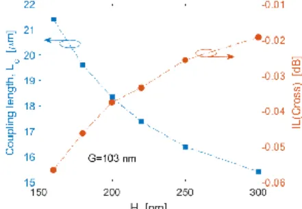
Let us now examine the influence of H changes on the switch performances. In this context, Fig. 7 shows the coupling length and the IL(Cross) as a function of the H parameter for a fixed waveguide gap, and assuming h = 80 nm. In particular we have adopted G = 103 nm, corresponding to the G0 value for H = 300
Fig.7. Coupling length and insertion loss as a function of the H parameter, for the 2×2 optical switch.In the simulations, G=103 nm, and h=80 nm.
The plot of Fig. 7 indicates that the coupling length decreases while increasing the values of H, resulting in an improvement of the device footprint. However, the opposite trend is recorded for the IL(Cross). Moreover, the increasing of H induces a reduction of the bandwidth (BW) as shown in Fig. 8, where the IL as a wavelength function is illustrated for different values of the H parameter, assuming h = 80 nm and G = 103 nm. Although the simulations have been carried out in the wavelength range from 1500 nm to 1600 nm, the curves are plotted in a smaller wavelength range in order to better evidence the IL values above -0.3 dB (this -0.3dB limit is used to define the switch BW in this paper). Similarly, Fig. 9 shows the relevant CT figure of merit.
The results of the parametric simulations are summarized in Table I, where other cases of interest (i.e. WL × HL = 500 nm ×
250 nm, G = 80 nm, H = 160 nm) are included (not explicitally
Fig. 8. Insertion loss for both Cross and Bar states as a function of the wavelength for different values of the H parameter, in the case of the 2×2 optical switch.In the simulation, G=103 nm, and h=80 nm.
Fig. 9. Crosstalk for both Cross and Bar states as a function of the wavelength for different values of the H parameter, in the case of the 2×2 optical switch.In the simulation, G=103 nm, and h=80 nm.
Fig. 10. Coupling length and insertion loss as a function of the H parameter, for the 1×2 optical switch.In the simulation, G=103 nm, and h=80 nm.
plotted in the figures for clarity). To the best of our knowledge, the values listed in Table I represent an important improvement of the performance for non-volatile optical switches with respect to the values proposed in literature. The IL listed in the Table is the mid-band value and the Cross state is chosen because it, rather than the Bar state, limits the performance.
It is worth outlining that only the second row case in Table I satisfies the condition IL(Cross)=IL(Bar). All other considered cases could require G values smaller than 80 nm. The plot of Fig. 8 and the results summarized in Table I demonstrate, as a general trend, that the switch metrics and the bandwidth improve if the design rule H<HL is followed for a given value
of G. As a result, a dual etching process must be implemented in order to fabricate switches with H<HL, which is an available
option in most industry-standard silicon photonic foundry processes. Although the complete power transfer in 2×2 switch occurs for the condition H=HL (as demonstrated by Fig. 5), here
we accept the increasing of fabrication complexity induced by
a dual etching process with the aim to of demostrate
demostrating the feasibility to of improve improving the switch metrics and bandwidth with respect to the state of art presented in literature. We note that such a dual etching process is now routinely offered in most silicon photonics foundries as part of the standard process design kit (PDK).On the other hand, if we adopt the constraint H=HL most straightforward for fabrication,
we could achieve similar levels of performance of those obtained with H<HL if a decrease of the gap between the
waveguides is considered. Indeed, assuming WL × HL = 500 nm × 220 nm, h = 80 nm, H=HL, and G= 50 nm, we record IL(Cross)= -0.06 dB, IL(Bar)= -2.2×10⁻³ dB at 1550 nm, BW=
72.58 nm and CT<-38.6 dB. In this sense, it seems more efficient to adopt the condition H<HL instead of to reducereducing the gap below 50 nm.
Similar systematic investigations have been performed for the 1×2 optical switch, based on the 2WG-coupler. The numerical results are condensed in Figs. 10 and 11, and lead to the same conclusions made for the 2×2 optical switch, although several comments about the switching performances are worth mentioning. In order to compare self-consistently both 1×2 and 2×2 optical switches, we keep fixed the cross section of the passive waveguide and the gap value between adjacent waveguides. In this context, Fig. 10 shows the coupling length and the IL(Cross) as a function of the H parameter, assuming WL × HL = 500 nm × 220 nm, h = 80 nm, and G = 103 nm. The
plot evidences that, by comparing 1×2 and 2×2 switches, the 2WG-coupler achieves shorter values of the coupling length, despite its slightly larger insertion losses.
In Fig. 11 (a) and (b) IL(Cross) and CT of the 1×2 switch are plotted as a function of wavelength. The results for the 3WG-coupler are also included for comparison. In the simulations we have assumed: WL × HL = 500 nm × 250 nm, H = 160 nm, h =
80 nm, and G = 80 nm. The values of Lc, IL(Cross) at 1550 nm,
and BW are 16.7 µm, -0.083 dB, and 95 nm, respectively. It is worth noting that the 2×2 architecture shows the values 23.63 µm, -0.06 dB, and 72.6 nm, respectively. Although the 1×2 switch presents a 22.4-nm larger bandwidth, this improvement is accompanied by a strong increase of crosstalk. The 2WG-coupler data show that, inside the bandwidth, the CT values range from -12.83 dB to -45.52 dB in the Cross state and from -47.96 dB to -52.79 dB in the Bar state. Better results are obtained for the 2 × 2 switch, where CT values changing from 33.84 dB to 82.11 dB in the Cross state and from 92 dB to -87.9 dB in the Bar state.
Fig. 11. (a) Insertion loss for both Cross states as a function of the wavelength; (b) Crosstalk for both Cross and Bar states as a function of the wavelength.
TABLEI
GEOMETRICAL AND SWITCHING PARAMETERS OF THE 2×2 SWITCH
Switching parameters W [nm] Lc [µm] BW [nm] IL(Cross) (1.55 µm) [dB] CT [dB] WL×HL=500nm×250nm; H=200nm; G=103nm 465.14 23.98 65.44 -0.048 <-36.5 WL×HL=500nm×220nm; H=300nm; G=103nm 354.75 15.40 58 -0.018 <-31.3 WL×HL=500nm×220nm; H=200nm; G=103nm 419.02 18.32 60.72 -0.037 <-34.4 WL×HL=500nm×220nm; H=180nm; G=103nm 442.9 19.60 61.78 -0.046 <-34.6 WL×HL=500nm×220nm; H=200nm; G=80nm 419.02 14.94 66.94 -0.032 <-33.5 WL×HL=500nm×220nm; H=160nm; G=80nm 474.79 17.43 70 -0.046 <-38.13 B. Thermal Simulations
In this sub-section we investigate the feasibility of inducing the phase change in GSST by means of Joule heating using an ITO electrode. In this context, we describe the amorphization mechanism by FEM models in COMSOL [29], using the 3WG-coupler designed in the previous section, in which an 80 nm GSST layer is deposited on an SOI strip waveguide having a cross section W × H = 474.79 nm × 160 nm and WL × HL = 500
nm × 220 nm. Moreover, a 50 nm layer of ITO is used to induce Joule heating, and the gap between the adjacent waveguides is set to 80 nm. In order to perform realistic thermal simulations, we have adopted a finite SiO2 cover thickness, assumed to be
reasonably ofrealistically 500 nm thick over the waveguide.
The switching to the amorphous state can be achieved by means of a voltage pulse with enough energy and trailing edge in the 0.5-5 ns range to rapidly melt-quench the GSST, thus favoring a disordered state [11]. As well detailed in [11], if Pmin is the minimum pulse power able to amorphize the PCM, then, any pump pulse with fixed width and power Pp ≥ Pmin is able to
induce amorphization, starting from the condition of the crystalline phase.
It is worth mentioning that under the approach presented in this work, the voltage pulse width and the electric pulse power are related to the electric conductivity of the ITO layer. A realistic value of the electrical resistivity for ITO with free carrier concentration of about 1 × 1019 cm-3 can be estimated as
ρ=0.0016 Ω × cm, according to the experimental measurements presented in [30]. To consider the time evolution of the temperature upon pulse excitation, we performed 3D multiphysics simulations where the heat transfer in solids model is coupled together with the electric currents model. The time dependent study is, thus, adopted to solve the coupled thermal and electric equations under the rectangle pulse voltage excitation. The input voltage pulse is 3 µs wide, centred at 2.5 µs (rise time of 0.5 ns, see Fig. 12). The design is therefore compatible with GSST switching given the improved Am phase stability of GSST [26]. To the best of our knowledge the
thermal parameters of GSST are not listed available in
literature, . Given the structural similarity between GSST and the classical GST alloy [26], so we use the GST values as a
good approximation to evaluate the switching
featurescharacteristics. The material properties used in the simulations are summarized in Table II. Our results demonstrate that the process of amorphization can be obtained with a 24 V pulse, raising the GSST temperature above the melting temperature of 900 K. The energy consumed during the process is estimated in as 146.97.0 nJ.
TABLEII
PHYSICAL PARAMETERS OF THERMAL SIMULATION
Materials Silicon dioxide Silicon Am-GSST Cr-GSST ITO Density [kg/m3] 2203 2329 ~6000 [11] 6150 [12]÷6300 [11] 7100 [11] Thermal conductivity [W/mK] 1.38 130 ~0.57 [31] ~1.58 [31] ~1340 [11] Heat capacity at constant pression [J/kgK] 746 700 212 [32] 212 [32] 11 [11]
Fig. 12 shows the maximum temperature (Tmax) inside the
O-PCM layer as a time function under rectangular voltage pulse excitation.
Spatial temperature distribution for the process of amorphization is shown in Fig. 13 (a), where the plane cross section placed in the middle of the O-PCM length (Lc = 17.4
µm) has been considered. Moreover, the temperature levels along the longitudinal axis of the O-PCM waveguide at both the bottom and the top surfaces of GSST layer are illustrated in Fig. 13 (b). The plot indicates clearly that the amorphization process starts to take place on the top and the middle of the GSST layer, where the temperature first reaches the melting value. Moreover, the simulations of Fig. 13 indicate that complete amorphization can be induced over the entire Lc = 17.4 µm for
the considered voltage pulse.
Similar investigations have been performed for the 1×2 switch having: W × H = 541.92 nm × 160 nm, h = 80 nm, G = 103 nm, and WL × HL = 500 nm × 250 nm. The results are
plotted in Figs. 14 (a) and (b).
Fig. 12. Maximum temperature in the O-PCM layer as a function of time for rectangular pulse heating.
Fig. 13. (a) Temperature distribution in the plane cross section placed at the middle of the O-PCM length in the case of 2×2 optical switch. (b) Temperature profile as a function of the londitudinal coordinate at the top and bottom O-PCM layer su
Fig. 14. (a) Thermal dostribution in the plane cross section placed at the middle of the O-PCM length in the case of 1×2 optical switch. (b) Temperature profile as a function of the londitudinal coordinate at the top and bottom O-PCM layer surface.
Fig. 15. Maximum and minimum temperature in the O-PCM layer as function of time for pulse-train heating.
It is worth noting that here a 24 V pulse of 2.5 µs duration is required to induce the complete amorphization, as a result of the different material distribution. The energy consumed during the process is estimated in as 122.48 5 nJ.
To induce re-crystallization, the GSST needs to be heated above the crystallization temperature (~ 523 K) but below the melting point, for a critical amount of time. Although the operative temperature is lower than the melting temperature, this process is demonstrated to be more challenging. Indeed, while a single
pulse is needed to induce the transition from crystalline to amorphous phase, several pulses are required for crystallization [26]. In this sense, we apply a pulse train consisting of 20 pulses with a period of 4 µs and duty cycle of 50% at 5 V. The energy consumed corresponding to the applied voltage is 425.58 6 nJ.
Thus, the maximum and the minimum temperature inside the O-PCM layer is recorded as a time function. The results are illustrated in Fig. 15, demonstrating that low energy consumption is required to induce the change from amorphous to crystalline phase. Regarding the 24 V pulse amplitude that induces amorphization (starting from Cr), there is a way to improve the switching performance significantly, i.e. by increasing the ITO doping of to the order of 1020 cm-3. Indeed,
assuming the an ITO resistivity ρ=4×10⁻⁴ Ω×cm (for carrier
concentration around 2×1020 cm-3 [27]), our simulations record
that the complete amorphization can be obtained with a voltage pulse of 24 V and 0.15 µs wide width or alternatively by means of a 12 V pulse having a duration of 2.9 µs. However, optical simulations indicate that for the ITO carrier concentration of 1020 cm-3, IL(Cross) is larger than 0.37 dB for G > 80 nm. Thus,
the best trade-off between conflicting requirements such as
switching performance and low IL, can be achieved under the
hypothesis to of designing a single switch. However, here we propose the design of the O-PCM switches under the perspective to of realize realizing a large-scale on-chip matrix switch, such as a Benes network. In this sense to preserve low IL, we elected not to pursue the high-doping strategy.
IV. CONCLUSIONS
In this paper, manufacturable on-chip nonvolatile broadband 1 × 2 and 2 × 2 switches are designed and analyzed theoretically. The switches consists of asymmetric two-waveguide and symmetric three-waveguide couplers in which the Cross or the Bar state is induced by setting the O-PCM in the amorphous or the crystalline phase, respectively. In each switch, the O-PCM is Ge2Sb2Se4Te1 deposited as top-cladding on one of the
coupled SOI strip waveguides. The photonics platform assumed in this work is the foundry-compatible and CMOS-compatible SOI platform operating in the telecommunication C-band. The passive waveguide are assumed to have a cross section of WL × HL = 500 nm × 220 nm or WL × HL = 500 nm × 250 nm. The
cross section of the active PCM have been chosen to satisfy the requirements of low insertion loss (less than 0.3 dB) over a large wavelength bandwidth, as a result of the parametric investigations. The O-PCM phase is changed by means of the ITO heater strip atop the O-PCM layer, inducing Joule effect as a result of applying voltage pulses.
The simulations have demonstrated the feasibility of obtaining O-PCM 2×2 switches with high performances across a large bandwidth ranging from 58 to 72 nm around 1550 nm. Moreover, all the devices have been designed to have the Cross state as limiting the switching performances. A representative example for the compact 15.4 µm coupling length is an IL(Cross) of -0.048 dB with CT lower than 38.1 dB over the 70-nm -0.3dB-IL bandwidth. The 1×2 architecture is even more compact, for which the coupling length changes from 11 µm to 16.7 µm. Regarding the switching condition, we find that a 24 V pulse of 2.9 µs (2×2 switch) and 2.3 µs (1×2 switch) in duration is required to raise the GSST temperature above the
melting temperature of 900 K in order to induce the amorphization process. Moreover, thermal simulations indicate that complete amorphization occurs over the entire O-PCM length. Complete crystallization is also possible by applying a pulse train of 20 or more pulses with a period of 4 µs and duty cycle of 50% at 5 V. This work represents an important improvement with respect to the performances of ultra-compact and non-volatile electro-optical switches reported in the literature.
ACKNOWLEDGMENT
R. Soref thanks Air Force Office of Scientific Research for sponsorship on grant FA9550-17-1-0354. Y. Zhang and JJ Hu acknowledge funding support provided by DARPA under Grant
# Number D18AP00070. V. Passaro thanks the support of Fondo di Ricerca di Ateneo.
REFERENCES
[1] M. Wuttig, H. Bhaskaran, and T. Taubner, “Phase-change materials for non-volatile photonic applications,” Nature Photonics 11(8), 465–476 (2017).
[2] D. Tanaka, Y. Shoji, M. Kuwahara, X. Wang, K. Kintaka, H. Kawashima, T. Toyosaki, Y. Ikuma, and H. Tsuda, “Ultra-small, self-holding, optical gate switch using Ge2Sb2Te5 with a multi-mode Si
waveguide,” Opt. Express 20(9), 10283–10294 (2012).
[3] T. Moriyama, H. Kawashima, M. Kuwahara, X. Wang, H. Asakura, and H. Tsuda, “Small-sized Mach-Zehnder interferometer optical switch using thin film Ge2Sb2Te5 phase-change material,” Optical Fiber
Communications Conference and Exhibition, San Francisco, USA, 2014,
p. Tu3E.4.
[4] H. Liang, R. Soref, J. Mu, X. Li, and W.-P. Huang, “Electro-optical phase-change 2 x 2 switching using three- and four-waveguide directional couplers,” Appl. Opt., vol. 54, no. 19, pp. 5897-5902 (2015). [5] M. Stegmaier, C. Ríos, H. Bhaskaran, C. D. Wright, and W. H. Pernice, “Nonvolatile all-optical 1×2 switch for chip scale photonic networks,”
Adv. Opt. Mater., vol. 5, no. 1 (2016)
[6] M. Rude, J. Pello, R. E. Simpson, J. Osmond, G. Roelkens, J. J. van der Tol, and V. Pruneric, “Optica switching at 1.55 µm in silicon racetrack resonators using phase change materials,” Appl. Phys. Lett., vol. 103, no.14, p. 141119 (2018).
[7] N. Ali and R. Kumar, “Design of a novel nanoscale high-performance phase-change silicon photonic switch,” Photonic Nanostructure, vol. 32, pp. 81-85 (2018).
[8] Q. Zhang, Y. Zhang, J. Li, R. Soref, T. Gu, and J. Hu, “Broadband nonvolatile photonic switching based on optical phase change materials: beyond the classical figure-of-merit,” Opt. Lett. 43, 94-97 (2018). [9] Y. Zhang, J. Li, J. Chou, Z. Fang, A.Yadav, H. Lin, Q. Du, J. Michon, Z.
Han, Y. Huang, H. Zheng, T.Gu, V. Liberman, K. Richardson, and J.Hu, “Broadband Transparent Optical Phase Change Materials,” CLEO: Applications and Technology 2017, San Jose, California, United States, 14–19 May 2017, ISBN: 978-1-943580-27-9, jTh5C.4.
[10] P. Xu, J. Zheng, J. Doylend, A. Majumdar, “Low-loss and broadband non-volatile phase change directional coupler switches,” Arxiv, pp.1-7 (2018)
[11] C. Rios, M. Stegmaier, Z. Cheng, N.Youngblood, C. D.Wright, W. H. P. Pernice, and H. Bhaskaran, “Controlled switching of phase-changematerials by evanescent-field coupling in integrated photonics [Invited],” Opt. Mat. Express, 8(9), 2455-2470 (2018).
[12] N. Ali, R. Kumar, “Mid-Infrared non-volatile Silicon photonic switches using Ge2Sb2Te5 embedded in SOI waveguide,” arXiv:1812.06117v1,
(2018).
[13] J. Song, S. Ghosh, N. Dhingra, H. Zhang, L. Zhou, and B. M. A. Rahman,”Feasibility study of a Ge2Sb2Te5-clad silicon waveguide as
a non-volatile optical on-off switch,” OSA Continuum, 2(1), 49-63 (2019).
[14] W. Jiang, “Nonvolatile and ultra-low-loss reconfigurable mode (De)multiplexer/switch using triple-waveguide coupler with Ge2Sb2Se4Te1 phase change material,” Scientific Reports 8(1), 15946
(2018).
[15] W. Jiang, “Reconfigurable Mode (De)Multiplexer via 3D Triple-Waveguide Directional Coupler with Optical Phase Change Material,” Journal of Lightwave Technology, Early Access, (2018)
[16] H. Liang, R. Soref, J. Mu, A. Majumdar, X. Li, and W. Huang, “Simulations of silicon-on-insulator channel-waveguide electro-optical 2×2 switches and 1×1 modulators using a Ge2Sb2Te5 self-holding layer,”
J. Lightwave Technol. 33(9), 1805–1813 (2015).
[17] Z. Yu, J. Zheng, P. Xu, W. Zhang, and Y. Wu, “Ultracompact electrooptical modulator-based Ge2Sb2Te5 on silicon,” IEEE Phot.
Technol. Lett., vol. 30, no. 3, pp. 250–253 (2018).
[18] W. J. Wang, L. P. Shia, R. Zhao, K. G. Lim, H. K. Lee, T. C. Chong, and Y. H. Wu, “Fast phase transitions induced by picosecond electrical pulses on phase change memory cells,” Appl. Phys. Lett., vol. 93, no. 4, p. 043121 (2008).
[19] S.H. Lee, Y. Jung, and R. Agarwal, “Highly scalable non-volatile and ultra-low-power phase-change nanowire memory,” Nature Nanotechnol., vol. 2, no. 10, pp. 626–630 (2007).
[20] A. V. Kolobov, P. Fons, A. I. Frenkel, A. L. Ankudinov, J. Tominaga, and T. Uruga, “Understanding the phase-change mechanism of rewritable optical media,” Nature Materials, vol. 3, no. 10, pp. 703–708 (2004)
[21] H. Zhang, L. Zhou, B. M. A. Rahman, X. Wu, L. Lu, Y. Xu, and J. Song, “Ultracompact Si-GST hybrid waveguides for nonvolatile light wave manipulation,” IEEE Photon. J. 10(1), 1–10 (2018).
[22] V. Weidenhof, I. Friedrich, S. Ziegler, and M. Wuttig, “Laser induced crystallization of amorphous Ge2Sb2Te5 films,” J. Appl. Phys., vol. 89,
no. 6, pp. 3168–3176 (2001).
[23] V. Weidenhof, N. Pirch, I. Friedrich, S. Ziegler, and M. Wuttig, “Minimum time for laser induced amorphization of Ge2Sb2Te5 films,” J.
Appl. Phys., vol. 88, no. 2, pp. 657–664 (2000).
[24] K. Kato, M. Kuwahara, H. Kawashima, T. Tsuruoka, and H. Tsuda, “Current-driven phase-change optical gate switch using indiumtin-oxide heater,” Appl. Phys. Exp., vol. 10, no. 7, art. 072201 (2017). [25] D. Kita, B. Miranda, D. Favela, D. Bono, J. Michon, H. Lin, T. Gu, and
J. Hu, "High-performance and scalable on-chip digital Fourier transform spectroscopy," Nature Commun. 9, art. 4405 (2018)
[26] Y. Zhang, J. B. Chou, J. Li, H. Li, Q. Du, A. Yadav, S. Zhou, M. Y. Shalaginov, Z. Fang, H. Zhong, C. Roberts, P. Robinson, B. Bohlin, C. Ríos, H. Lin, M. Kang, T. Gu, J. Warner, V. Liberman, K. Richardson, J. Hu, ”Extreme Broadband Transparent Optical Phase Change Materials for High-Performance Nonvolatile Photonics, arXiv:1811.00526. [27] Z. Ma, Z. Li, K. Liu, C. Ye, and V. J. Sorger, “Indium-Tin-Oxide for
High-performance Electro-optic Modulation,” Nanophotonics, 4, pp. 198–213 (2015).
[28] B. Troia, F. De Leonardis, V. M. N. Passaro, ”Generalized modelling for the design of guided-wave optical directional couplers”, Optics Letters 39 (5), 1161-1164 (2014).
[29] Comsol Multiphysics, COMSOL AB, ver. 3.2 (2005), single license. [30] Y. Gui, M. Miscuglio Z. Ma, M. T. Tahersima, S. Sun, R. Amin, H. Dalir,
and V. J. Sorger, “Towards integrated metatronics: a holistic approach on precise optical and electrical properties of Indium Thin Oxide,” arXiv:1811.08344.
[31] E. Bozorg-Grayeli, J.P. Reifenberg, K.W. Chang5, M. Panzer, and K.E. Goodson, “Thermal conductivity and boundary resistance measurements of GeSbTe and electrode materials using nanosecond thermoreflectance,” 978-1-4244-5343-6/10, IEEE (2010). [32] P. K. Khulbe, X. Xun, and M. Mansuripur, “Crystallization and
amorphization studies of a pulsed laser irradiation,” Appl. Opt. 39, 2359– 2366 (2000).