Characterization and Modeling of Uniformity in
Chemical Mechanical Polishing
by Charles Oji
Submitted to the Department of Electrical Engineering and Computer Science in partial fulfillment of the requirements for
the degree of Master of Engineering
at the
MASSACHUSETTS INSTITUTE OF TECHNOLOGY January 22, 1999
© Massachusetts Institute of Technolo 8. All Rights Reserved.
A uthor ... ... ... Dep!haieny'of'Electrical Engineering and Computer Science
January 1999
Certified by .-... ...
Associate Professor of Electrical Engineering and Nmputer Science Department of Electrical Engineering and Computer Science Prof. Duane Boning
Certified by ... ... ... -... --Associate Professor ojO1trical Engineering Departm t of Electrical Engineering and Computer Science - -Prof. James Chung
Accepted by ...
of. Arthr C. Smith
Chairman, Department Committee on Graduate ThesesCharacterization and Modeling of Uniformity in
Chemical Mechanical Polishing
by
Charles Oji
Submitted to the Department of Electrical Engineering and Computer Science in partial fulfillment of the requirements for the degree of Master
of Engineering in Electrical Engineeering and Computer Science
Abstract
Chemical Mechanical Polishing (CMP) has become the preferred planarization method for multilevel interconnect technology because of the high degree of feature-level planarity it achieves. Methods are needed, however, to understand and model both wafer-level and die-wafer-level uniformity in polishing. This thesis first contributes an analysis of wafer-level uniformity models as a function of measurement pattern and number of sam-ple points. In particular, a grid pattern with at least 30 samsam-ples is found to result in good wafer level models. Second, this thesis examines the variation of die-level planarity across the wafer. Substantial dependency of planarization length (a characteristic length which determines die-level planarity) on die position is found, with planarization length in an experimental oxide polish process varying from 5.0 mm to 8.6 mm across the wafer. Finally, the wafer-level and die-level uniformity are both found to depend on process con-ditions such as table speed and down force. Together, these results demonstrate that wafer-level variation must be considered carefully in the modeling and optimization of unifor-mity in chemical mechanical polishing.
Thesis Supervisor: Duane Boning
Title: Associate Professor of Electrical Engineering and Computer Science
Thesis Supervisor: James Chung
Acknowledgements
I would like to express my sincere gratitude to my research advisors Professor
Duane Boning and Professor James Chung for their guidance and support throughout this
research. I would also like to thank my colleagues who were or are in the Statistical
Metrology Group for their support. Specifically, I would like to thank Dennis Ouma (a.k.a
the bit-level guru), Rajesh Divecha, Brian Stine, Taber Smith, Brian Lee, Tamba Tugbawa,
Jung Yoon and Vikas Mehrotra. I would like to thank Dennis Ouma, Brian Lee and Taber
Smith for their intellectually stimulating discussions, Tamba Tugbawa and Jung Yoon for
experimental data acquisition and Huy Le for his UNIX expertise. In addition to those
mentioned above, I would like to thank Abraham Seokwon Kim, Wenjie Jiang and Arifur
Rahman for their friendship. Furthermore, I would like to thank members of the
Microsys-tems Technology Laboratories for their various technical support.
My research has involved collaborations with people in industry and I would like
to thank them for their support. This thesis owes thanks to the following people and
orga-nizations who have contributed in many aspects of the research. This includes Warren Lai
and Alvaro Maury from Lucent Technologies, Bell Labs, Ann Westerheim and Daniel
O'Connor from Intel, Joseph Davis and Simon Fang from Texas Instruments, Jeffrey
Knecht from Lincoln Laboratories, Tony Pan from Applied Materials and many others
whom I have unintentionally omitted.
I would also like to express my gratitude to friends for their support and friendship.
Table of Contents
1 Introduction...11
1.1 Background...11
1.2 Uniformity Issues in Oxide CM P Processes... 12
1.3 Overview of Statistical Metrology and Contribution of Thesis...13
2 Variation of Uniformity Models with Spatial Distribution and Number of Sample Points... 19
2.1 Introduction... 19
2.2 Experimental M ethodology and Raw Data...20
2.3 Determination of Non-Uniform ity... 24
2.4 Results...26
2.5 Discussions and Suggestions for Improvem ent ... 28
2.6 Conclusions... 30
3 Variation of Planarization Length with Process Conditions and W afer Edge Effects... 32
3.1 Introduction...32
3.2 M ethodology ... 33
3.3 Analysis Results...38
3.4 Discussion...46
3.5 Conclusion and Future W ork... 51
4 Conclusions and Future W ork ... 52
4.1 Summ ary ... 52
4.2 Improvements in Non-uniformity Modeling and Planarization Length Extraction ... 53
4.3 Future W ork ... 53
Appendix A Experim ental Rem oval Rate Data ... 57
List of Figures
Figure 1.1: CMP Polishing Machine (Rotary Configuration) ... 12
Figure 1.2: Wafer Level and Die Level Non-Uniformities...13
Figure 1.3: Definition of terms in polishing ... 14
Figure 1.4: Phases of Statistical Metrology Development as Applied to Oxide Thickness and CMP Variation...17
Figure 2.1: Different Samples of the Circular Pattern ... 21
Figure 2.2: Different Samples of the Grid Pattern... 22
Figure 2.3: Different Samples of the Radial Pattern...23
Figure 2.4: Surface Plot of the Removal Rate on a Typical Wafer ... 23
Figure 2.5: Variation of Non-Uniformity Standard Deviation and Mean with the Number of Samples ... 27
Figure 2.6: Weighting Function Modification to MRS Model...29
Figure 3.1: Layout mask used in wafer processing; Density Mask ... 34
Figure 3.2: Die Positions on a W afer... 36
Figure 3.3: Definition of terms used in model...37
Figure 3.4: Experimental Extraction of Planarization Length...38
Figure 3.5: Effect of a Change in Table Speed and Down Force on Planarization Length... 39
Figure 3.6: Surface Interpolation of Planarization Lengths (Table Speed/Down Force levels indicated)... 41
Figure 3.7: Planarization length variation with process conditions...42
Figure 3.8: Summary of the Effect of Table Speed and Down Force on Average Planarization Length... 43
Figure 3.9: Blanket rates for different process conditions...45
Figure 3.10: Summary of the Effect of Table Speed and Down Force on the Mean and Standard Deviation of Removal Rate ... 47
List of Tables
Table 2.1: Multiple Response Surface Modeling ... 24
Table 2.2: Error in the computed non-uniformity for various numbers of samples ... 28
Table 2.3: Effect of Weighting Function on Non-Uniformity ... 30
Table 3.1: CM P Process Conditions ... 35
Table A. 1: Experimental Data (Removal Rates) for all the Wafers ... 57
Table A.2: Experimental Data (Removal Rates) for all the Wafers ... 71
Table B.1: Planarization Lengths on Different Dies Per Wafer for M /M Process Condition ... 87
Table B.2: Planarization Lengths on Different Dies Per Wafer for L/L Process C ondition... 88
Table B.3: Planarization Lengths on Different Dies Per Wafer for H /H Process Condition... 89
Table B.4: Planarization Lengths on Different Dies Per Wafer for H /L Process Condition ... 90
Table B.5: Planarization Lengths on Different Dies Per Wafer for L/H Process Condition ... 91
Chapter 1
Introduction
1.1 Background
Chemical Mechanical Polishing (CMP) has become the chosen planarization
method for advanced multilevel interconnect technology. Engineers and researchers are
aware of how important it is to eliminate particles from the cleanroom but even though
CMP involves the introduction of particles through the use of slurry, it is popular because
it offers the best planarization performance to date. Although CMP achieves good
feature-level planarity, there is still much to be discovered and improved in CMP. Understanding
of die-level and wafer-level uniformity issues is needed. In addition, the polish evolution
of dies at the edge of the wafer is still to be investigated and the polishing characteristics
of metals such as copper and tungsten still need to be modeled [8].
Figure 1.1 illustrates a typical example of a CMP machine set-up. Although this
machine has one head, multiple-headed machines are also available. During the polishing
process, the wafer is held face down using tdown force on the carrier spindle. The wafer is
then polished by the rotating head of the carrier pressed against the rotating platen (table).
The rotating platen contains a polyurethane pad with a slurry of colloidal silica within an
aqueous solution suspension. Slurries of varying selectivities (that is with different
chemi-cal compositions) are used in polishing the metal and other films. The polishing action is
brought about by the different rotating axes of the carrier and table, even though they are
rotating in the same direction. The polishing action is primarily achieved through the
com-bination of mechanical forces created by the exertion of the pad on the colloidal silica
to wear and the polish rate diminishes. However, this problem can be alleviated by
condi-tioning the pad surface with a diamond-tipped conditioner. The most common machines
are of rotary type but linear machines are being explored because of their high speed
alter-native pad approaches [4], which may improve die and wafer-level performance.
Wafer held by holder
Slurry Feed Feed
Platen
Carrier Polishing Pad Platen
(head)
(a) Side View (b) Top View
Figure 1.1: CMP Polishing Machine (Rotary Configuration)
1.2 Uniformity Issues in Oxide CMP Processes
This thesis analyzes two types of uniformities, namely wafer-level uniformity and
die-level uniformity. The former is characterized by the variation in some parameter (e.g.,
oxide thickness) on the wafer scale. Die-level uniformity, on the other hand, is restricted to
die-level while Figure 1.2 (b) shows the wafer-level equivalent.
(a) Die-Level Non-Uniformity (b) Wafer-Level Non-Uniformity
x 10 -13000., 1.4-*120W0 911000. S10000. 9 000. 7 000. 6000 20 3 1.2.. ~ 0.8.. 15 20 50 10 is 0 5 - 50
y-location (mm) 0 0 x-Iocation (mm) y-location (mm) -100 -100
Figure 1.2: Wafer Level and Die Level Non-Uniformities
100 50 0
x-locatIon (mm)
CMP planarization of oxide results in good short-range planarity (on the scale of a
few microns) compared to other planarization techniques such as oxide reflow or resist
etchback, but remains hampered by systematic pattern sensitivities. Excellent global
uni-formity in CMP processes is crucial since the feature size of present microelectronic
struc-tures is shrinking and multilevel interconnect technology requires excellent planarity to
achieve lithographic depth of focus requirements. The need for good uniformity has
moti-vated the study of how to better model uniformity in oxide CMP processes and how
non-uniformity affects the planarization length at different die positions on a wafer. Uniformity
concerns have also motivated the study of the effect of different process conditions such as
table speed and down force on planarization length. Recent literature shows that the
pla-narization length does increase with relative polishing speed and decrease with down force
[4].
1.3 Overview of Statistical Metrology and Contribution of Thesis
Fig-Before CMP
Loca
Step
Heigh
After CMP
|iO2
Planarization Lent IGlobal
StepHeight
Figure 1.3: Definition of terms in polishing
ure 1.2, the local step height is the difference between the heights of the up and down areas
(before planarization) and the global step height is the same difference except after
pla-narization has been achieved. Ideally, the raised areas are polished without any polishing
of the down areas but in actuality there is a small amount of polishing that takes place in
the down areas and this varies with the width of the down area. However, if the width of
down area is much less than the planarization length of the pad, there is negligible down
area polishing because the polish pad cannot fold into the down areas. This is the primary
reason for the good planarity that is achieved with CMP. Some important parameters can
be defined as follows:
planarization length: the length scale over which layout density affects local pla-narization rate [5]
rate of local planarization: rate of step height reduction with time
Total Indicated Range (TIR) or global step height reduction: the difference between the highest and lowest points on the die.
Due to the capability of CMP to planarize most of the local features, step height
reduction capability is not the main factor to be assessed in CMP. On the contrary, the TIR
for a die gives a good measure of the global planarization performance for a particular set
of process conditions with a given set of consummables. However, the disadvantage of
using TIR as a metric of merit is that its value is unpredictable for different layouts except
those for which it is determined. The planarization length is a more comprehensive
char-acterization parameter because given the planarization length for a process, the TIR may
be obtained for any layout that is polished under identical process conditions [14]. CMP
still has problems associated with it, namely pattern dependent thickness variation which
manifest as global (but within-die) thickness variation. Other problems include
wafer-scale variations in removal rate across a wafer because of macroscopic wafer-wafer-scale process
variations which are superimposed on the within-die variation.
Statistical metrology is the body of methods for understanding variation in
micro-fabricated structures, devices, and circuits. It is a bridge between manufacturing and
design. The Statistical Metrology Group at MIT has made a significant contribution in the
characterization and modeling of CMP processes. In the beginning, there was an emphasis
on the characterization of variation, not only temporal (e.g. lot-to-lot or wafer-to-wafer
drift), but also spatial variation (e.g. wafer, and particularly chip or
within-die). A second important defining element is a key goal of statistical metrology: to identify
the systematic elements of variation that otherwise must be dealt with as a large "random"
systematic, repeatable, or deterministic contributions to the variation from sets of deeply
confounded measurements. Such variation identification is critical to focus technology
development of device or circuit design rules which minimize or compensate for the
varia-tion [10, 12, 13].
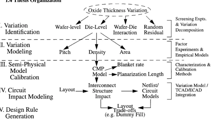
The development of CMP characterization and modeling has evolved through five
channels as shown in Figure 1.3 [1]. These phases are variation identification, variation
modeling, semi-physical model calibration, circuit impact modeling and design rule
gen-eration. These methods come about to tackle the problem created by ILD thickness
varia-tion after CMP. Variavaria-tion identificavaria-tion involved screening experiments and variavaria-tion
decomposition methods to separate and identify the components of oxide thickness
varia-tion. Phase II involves developing models of the variation in phase I. These methods
include factor experiments and empirical experiments, which result in models with a
func-tional dependency on particular layout practices (e.g. the density, pitch, or area of layout
structures). In the oxide CMP case, density was found to be the primary explanatory
fac-tor, enabling the development of semi-physical modeling for oxide polishing in phase III.
Here, it is important to create tightly coupled characterization and calibration methods for
extraction of model parameters such as blanket removal rate and planarization. This is
where this thesis makes its contribution.
The central focus of this thesis is to study how well CMP planarizes and how to
optimize data collection for more efficient modeling to better understand wafer-level and
die-level non-uniformity. In addition, we will study wafer-levelnon-uniformity effects on
planarization length. The latter eliminates the unverified assumptions made in the past that
con-dition. Wafer-level uniformity is affected by process conditions such as table speed, down
force and slurry selectivity; errors in uniformity models arise from variations in the
num-ber and method of data collection used to obtain these models [4].
1.4 Thesis Organization
6 Oxide Thickness Variation,
AK Screening Expts.
I. Variation Wafer-level Die-Level Wafer-Die Random & Variation
Identification Interaction Residual Decomposition
II. Variation Factor
Modelng D~jisAreaExperiments &
Modeling Pitch De sity Area
Empirical Models
III. Semi-Physical lanket rate Characterization
Model CMP----W e Calibration
SModel -- Planarization Length Methods
Interconnect Netlist/ Variation Model /
IV. Circuit Layout lp. Structure - Circuit TCAD/ECAD
Impact Modeling Impact Models
J
IntegrationL-1.Layout
V. Design Rule Trade-offs
Generation (e.g. Dummy Fill)
Figure 1.4: Phases of Statistical Metrology Development as Applied to Oxide Thickness and CMP Variation
This thesis is divided into four main sections. In addition to the introduction,
which gives a brief overview of statistical metrology, the contribution and organization of
this thesis, Chapter 2 presents the methodology part of this work. In Chapter 2 we look at
how to minimize the amount of data required for accurate wafer-level uniformity
model-ing. In Chapter 3, we identify the effect of wafer-level oxide thickness variation (i.e.,
wafer-level non-uniformity) on planarization lengths and how process conditions affect
planarization lengths. Chapter 4 then summarizes the main body of this thesis together
with suggestions for improvement and extension of the work. The appendices present
detailed data and experiments associated with wafer-level uniformity modeling (Appendix
A), as well as data related to planarization length as a function of die position (Appendix
Chapter 2
Variation of Uniformity Models with Spatial
Distribu-tion and Number of Sample Points
2.1 Introduction
Wafer-level uniformity has become a very important factor in semiconductor
pro-cesses. Reliable methods of modeling non-uniformity already exist; however, these
mod-els are not currently being applied efficiently. The Multiple Response Surface (MRS)
method [2] is used to compute the non-uniformities on various wafers for different
num-bers of measurements and as a function of process conditions. Additional methods are
available for modeling of the spatial level surface in addition to computing a
wafer-level uniformity metric [3]. This thesis proposes a solution that will efficiently apply the
MRS to non-uniformity metric modeling. Specifically, we show how the measurement
dis-tribution (location in space) and number of measurements will affect the non-uniformities
calculated [2]. Hence for a given error tolerance, only the minimum number of
measure-ments is required. Measuremeasure-ments are often taken on a wafer without a prior quantitative
knowledge of the degree of accuracy achievable using a non-uniformity model, a spatial
sampling pattern and a given number of measurements.
This study investigates how the non-uniformity metric values obtained from MRS
models deviate from their true values as the number of sample points on the wafer is
var-ied. Furthermore, the variation with different sampling or measurement patterns will be
investigated. A quantitative measure of how accurate the non-uniformity models are for
different sampling patterns and number of measurements will increase efficiency. This is
measure-ments needs to be taken on a wafer to achieve a desired accuracy, with a corresponding
time savings.
This chapter has been divided into sections to explain the experiments and analyses
performed to arrive at the conclusions. Chapter 2.2 explains the processes which the
wafers underwent before and after polishing and the method of analyzing the data;
Chap-ter 2.3 gives the theoretical basis of the non-uniformity metric. The results are presented in
Chapter 2.4 and discussions in Chapter 2.5. The final section summarizes our conclusion.
2.2 Experimental Methodology and Raw Data
A process sequence was performed to deposit silicon on the blanket wafers prior to
Chemical Mechanical Polishing (CMP) on 200 mm diameter wafers. A blanket deposition
of LPCVD TEOS then followed. The wafer lot used in these experiments were polished
on a rotary system (IPEC/Planar) at conventional speeds using the IC1400 polishing pad.
The down force ranged from 4.8 psi to 8 psi; the table speed range was from 32 rpm to 80
rpm and the carrier speed range was from 28 rpm to 60 rpm. Optical oxide film thickness
measurements were taken before and after CMP; together with the polish time, the
removal rates were computed. In the next section, a detailed description of how the
non-uniformity metric was computed from the raw data is given.
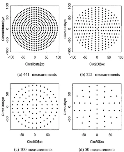
A total of 441 oxide thickness measurements were taken using the circular pattern
shown in Fig. 2.1. The actual measurements are shown in Appendix A. These measure-ments form the detailed "baseline" dataset from which we select subsets of data to study other sampling patterns. For example, the circular pattern with 221 measurements was obtained by taking every other point on the first pattern with 441 points. By reusing the same data but in a subset fashion, we avoid the introduction of additional data measure-ment noise as we compare one sampling pattern against another. The same method was
applied to the 221 point circular pattern to get the 100 point circular pattern and a similar method on the 100 point pattern yielded the 50 point pattern, as illustrated in Figure 2.1.
o 0
o2 ::: :: o:::...''.. <g . ' - - 0 * *
-100 -50 0 50 100 -100 -50 0 50 100
Circalldata$xc Circ200$xc
(a) 441 measurements (b) 221 measurements
0000 0 * .000. * - --50 0 5-0 0 0 (c) 0.00 mesrmet0d 50 meaureent 0 0 0 U.) 00 0 0 0 0 0 0 0 U? Ff of0 th 0 0atte 10 -5S 0 00 50 0 050 0 5 0
mesuemn poits asilutaued nt igur 2.3.aurmet
0 0.. 0 00 -50 0 50 -50 0 50 CirclOO$xc Circ5O$xc (c) 100 measurements (d) 50 measurements
Figure 2.1: Different Samples of the Circular Pattern.
The radial pattern was generated by dividing the wafer area into eight parts separated
by 45 degrees and taking those points that lie along these lines of separation. The first
radial pattern has 81 measurement points. The second radial pattern was obtained from the first by taking every other point on the first pattern. The same method was applied to the 41 measurement points on the second radial pattern to generate the third pattern with 20
measurement points, as illustrated in Figure 2.3.
The grid pattern was generated by interpolating over all the circular measurements. The largest grid pattern has 448 measurement points. The second largest grid pattern was generated by taking every other point on the x-axis and every other point on the y-axis of
the largest grid pattern. The same technique is applied to the 112 points of the second grid pattern to get the 30 points on the third pattern. A similar method is used to extract 8 points for the last grid pattern, as illustrated in Figure 2.2.
0. LO LO 0 0 C 0 LO -50 0 50 newalldata$xc (a) 448 measurements -50 0 50 newdata31$xc (c) 31 measurements -50 0 50 newdatal 12$xc (b) 112 measurements Cu5 0 0 (0 (0 0 ItJ 0 0 -80 -60 -40 -20 0 20 40 newdata8$xc (d) 8 measurements
Figure 2.2: Different Samples of the Grid Pattern
000000 000000000000 00000000000000 00 00 0000000 00000 00000 000 0000 00 000 0 00000000000000000000 0000000000000000000000 0000000000000000000000 0000000000000000000000 000000000000000000000000 000000000000000000000000 000000000000000000000000 000000000000000000000000 000000000000000000000000 000000000000000000000000 0000000000 000000000000 0000000000000000000000 0000000000000000000000 00000000000000000000 000000000000000000 0000000000000000 00000000000000 000000000000 000000 LO) 0 0 LO CO 0 0 * 0 0 * 0 0
0 '0 CO 0 0 LO 0 0 0 o 0 L 0-om CO Ca o o? 0 50 100 -100 Radial80$xc (a) 81 measurements -50 0 50 100 Radial4O$xc (b) 41 measurements 0 0 o-o . *0 Ca Lt) 0 -100 -50 0 50 100 Radial20$xc (c) 20 measurements
Figure 2.3: Different Samples of the Radial Pattern
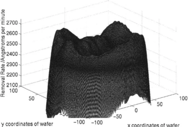
Surface Plot of the Removal Rate on a Typical Wafer
E 2700 a) 02600. U) 22500- C02400-w 2300 2200 o 02 1 0 0 -M 100 mr 50 100 50
y coordinates of wafer x coordinates of wafer
Figure 2.4: Surface Plot of the Removal Rate on a Typical Wafer
. * * 5 0 * 0 0 * 5 0 * 0 0* 0 5 5 0 -..:,.' .. . . .0 -100 LLO 0 * . . . . * . . . -0 -50 01
As an example of the wafer-level observed, Figure 2.4 shows the surface plot of the
441 removal rates of the circular pattern. It should be expected that different sampling
pat-terns and sample point densities will result in different values for non-uniformity.
2.3 Determination of Non-Uniformity
Based on the measurement patterns described above, we want to compare how the
non-uniformity metric varies depending on this plan. In this section we describe the
Multi-ple Response Surface which we will use to compute non-uniformity. In Chapter 2.4 we
then apply it to our experimental data.
Table 2.1: Multiple Response Surface Modeling
Process P1 P2 d1 d2 ... rrdN G
Split t
1 Si1 S12 rri1 1 IT12 ... I1N
(a)1
2 S21 S22 rr21 T22 ... 2N
n Sn1 Sn2 rrn1 irn2 . nN
The Multiple Response Surface method can be illustrated using Table 2.1. In this
table, P1 and P2 are process setting, rrdN is the removal rate at the position of die N, N is
the number of dies on a wafer, n is the number of process splits and S, is the process
set-ting for process factor Py and process split x. In the Multiple Response Surface method,
process factors. For example, the values in the 4th column in Table 2.1 (rrdl) are regressed
over the process settings in the second and third columns (S11 and S12) to get the following
die site model:
drr, = a + P1 + yP2 + tP1.P2 (1)
where drrx is the removal rate at the position of die x as a function of the process
conditions and a, P, y and T are constants found by the regression. Consequently, the
removal rate for any die position at known process settings (that is, known values of P1
and P2) can be calculated. The non-uniformity metric is a/g and can be computed from
the following definitions for the estimated mean and standard deviation:
= $(drr + drr2 + ... + drrN) (2) and
-= (N- 1) (drr - )2 ... + (drrN _) 2
(3)
The non-uniformity is often reported as a percentage, or 100 a/p.
Non-uniformity can be computed using either the final oxide thicknesses or the
removal rates. The removal rates are useful in the case where the wafers are not totally
uniform before polishing because the removal rate takes into account the fact that the
2.4 Results
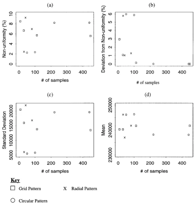
We first consider the trend in estimated non-uniformity for each of the sampling pat-terns considered, as a function of the number of samples. Looking at Figure 2.5 (a), the apparent non-uniformity decreases as the number of sample points increases in the case of the grid pattern. In other words, if the grid pattern is used for taking measurements, fewer measurements will infer that the wafer surface is less uniform than it actually is. On the other hand, when the circular pattern and the radial pattern are used for taking measure-ments on the wafer, the fewer the number of measuremeasure-ments the more uniform the wafer surface appears to be.
The grid-based estimates appear to converge to a constant value as the number of points increases. In addition, the circular pattern converges but to a different value. This is likely because the circular pattern may effectively weight different regions of the wafer more heavily or differently, so depending on the underlying spatial pattern different sam-pling patterns may result in different uniformity values.
From Figure 2.5 (b), the change in non-uniformity with the number of samples for
the grid pattern varies at a lower frequency compared to the change observed with the radial and circular patterns. Again looking at Figure 2.5 (b), the non-uniformity in the case
of the grid pattern varied over the smallest range of number of samples compared to the radial and circular patterns. There was no clear difference observed when comparing the non-uniformity range for the radial and grid patterns.
A look at the plots for the mean of the MRS models in Figure 2.5 (c) shows the opposite variation compared to that observed in the non-uniformity which is in accordance
with the fact that non-uniformity is inversely proportional to the mean. On the other hand,
10 0 0 z C 0 C C, 0 100 200 300 # of samples (a) x 0 o o 0 0 0 X0 o 0 100 200 300 400 # of samples (c) x 00 00 0 x, , 0 ,, 400 (0 LO C\I C0 10 0 =3 0 z E 0 0 C U) (b) XO0 0 OX X 0 o 0 100 200 300 400 # of samples (d) X 0 0 XO 0 0 0 0 0 x 0 100 200 300 400 # of samples Key
E
Grid Pattern X Radial Pattern0 Circular Pattern
Figure 2.5: Variation of Non-Uniformity Standard Deviation and Mean with the Num-ber of Samples
itself. Since the standard deviation dictates the trend in the non-uniformity with number of
samples, it does suffice (as expected) to only look at the standard deviations. This is
sim-ply because the standard deviation is a constant multiple of the non-uniformity or can equally be viewed as the spread from the mean value.
From the graph of non-uniformity versus the number of samples in Figure 2.5 (a), 0) C0 0 0) LO c"j 0) 0) 0) 0t C~j 0) 0) 0) 0> CO) C~j
the error in the computed non-uniformity for various numbers of samples is summarized
in Table 2.2.
Table 2.2: Error in the computed non-uniformity for various numbers of samples
Sample # of samples Error (%) Distribution 441 0.000 Circular 221 0.007 50 5.985 448 0.000 Grid 112 0.140 30 1.078 81 1.250 41 5.800 Radial 20 1.050
2.5 Discussions and Suggestions for Improvement
The grid pattern seems to offer the best results for the CMP conditions and wafer
data considered. Not only does the grid pattern result in a smoothly varying
non-unifor-mity for different numbers of samples but the deviations from the actual non-unifornon-unifor-mity is
the least among other patterns. If a 1% deviation from the correct non-uniformity is
tolera-ble, only 35 grid measurements are needed instead of 205 circular measurements. The
next best results were obtained for the circular pattern which requires about 205 points to
give an error no more than 1%. The radial pattern gave the worst results. The discrepancies
apparently come from the way the measurement sites are distributed on the wafer surface.
The more reliable results of the grid pattern can be attributed to how well each grid site
radial pattern is significantly attributable to the highly irregular area representation of the
radial measurements. However, these problems can be minimized using the methods in the
next paragraph.
The reliability of these wafer-level uniformity results can be improved by using a
more sophisticated spatial modeling approach beyond using linear regressions to find
rela-tions between the removal rate at a particular die position and the process condirela-tions, and
then computing mean and standard deviation. Thin-plate splines are very useful functions
that may correct the biasing that is manifest in our results. As an alternative
approxima-tion, a weighting function can be applied to the experimental data to appropriately
stan-dardize the data for the unequal area representation of the measurement sites [3].
In order to explore the effect of area representation, a weighting function method
was used on the largest data set (that is, the 441 circular measurement points). Each point
was weighted using the area of the sector surrounding it as shown in Figure 2.6.
This area, Al, is associated with measurement point 1
Figure 2.6: Weighting Function Modification to MRS Model
The measured removal rates were then scaled by the ratio of the area of the sector to
compares the results of using and not using the weighting function. Please note that all
previous non-uniformity computations have been done without the weighting function
approach. Using the weighting function approach involves scaling the removal rates, for
Table 2.3: Effect of Weighting Function on Non-Uniformity
441 Circular Pattern Measurement Points
With Weighting Function 8.20%
Without Weighting Function 6.75%
example, the removal rate at the location of "point 1" (rr1) in Figure 2.5 is:
rr1 = (A, * drr)/A
where A, is the area associated with "point 1", drr, is the original removal rate at the
loca-tion of "point 1" and A is the area of the wafer without the 6mm exclusion region.
2.6 Conclusions
Our results show that the grid pattern is the most reliable sampling pattern of
mea-surements on a wafer for non-uniformity analysis, for the experiments considered here.
The next best distribution is the circular pattern and unless reasonable accuracy is not
essential, radial distributions can be used. A summary of these results are presented in
Table 2.2. With the incorporation of thin-plate splines and a weighting function to account
for the area representation of the wafer, the wafer non-uniformity analysis is expected to
Chapter 3
Variation of Planarization Length with Process
Condi-tions and Wafer Edge Effects
3.1 Introduction
Planarization length is a very important parameter in the characterization of oxide
and Shallow Trench Isolation (STI) Chemical Mechanical Polishing (CMP) processes.
This chapter utilizes several statistical and modeling techniques to help understand how
planarization length varies across process conditions, as well as within a given wafer. The
effects of downforce, table speed, and die position on planarization length have been
char-acterized. Even with a 6mm edge exclusion during processing, our analysis reveals that
die position plays a crucial role in the value of the planarization length. The die-to-die
variation of the planarization length within a wafer can be as much as 3.2 mm, compared
to an average planarization length of about 7.5 mm for the process we examined. In
partic-ular, the die at the opposite end of the wafer notch consistently exhibited the lowest
pla-narization length. The characterization results also show that the plapla-narization length
increases with table speed and decreases with downforce.
CMP of inter-layer dielectrics results in excellent feature-level planarity, but is also
affected by systematic pattern sensitivities. In the past, we have always assumed
planariza-tion length was approximately uniform across a wafer. This is because planarizaplanariza-tion
length is mainly determined by the polish pad type, the relative speed of the pad and
wafer, the down force, and other process parameters. However, in the 8" wafer era, the
longer holds. Now we are in a better position to predict the planarization length of a CMP
process at a specific die position which is useful in ULSI technology circuit design and
layout. It is important to use the correct planarization length because planarization length
is used to determine the correct effective pattern density. For example, a large
planariza-tion length across a wafer corresponds to a low effective pattern density range across all
the dies on the wafer; therefore, if the planarization length is not the same on all the dies
then the effective pattern density range will vary across the wafer. Consequently the
cor-rect planarization length is necessary to predict the corcor-rect Total Indicated Range (TIR)
[1].
This chapter has been divided into Chapter 3.2 which describes the experimental
plan and the analysis method, Chapter 3.3 where we present our data analysis and Chapter
3.4 which discusses the results. Chapter 3.5 summarizes our findings and describes future
projects.
3.2 Methodology
This section will give an overview of the experimental setup and the processing
conditions the wafers underwent, then the analysis method will follow. The latter will
detail the theoretical approach used to analyze the measure data on the processed wafer.
Experimental Setup
A total of 15 8" wafers underwent the following processing sequence. The short
loop test monitor used for this evaluation consisted of a combination of PETEOS and HDP
a blanket PETEOS film of 7500
A on 200 mm substrates. The initial dielectric step height
measured ranged from 0.92 gm to 0.94 gm across the two test lots processed. The initialILD thickness before CMP was between 2.65 gm and 2.7 gm. A target of 1.0 gm
dielec-tric removal from the 100% density structures was used to define the planarization target
time when the entire step height should be removed from all structures. Figure 3.1 shows
the 12mm density mask from the MIT characterization mask set that was used for the
metal patterning [4]. The 12mm mask has a 1mm buffer region and 25 square density
blocks, each 2mm in dimension. The densities increase in steps of 4% from a density of
4% in the bottom left corner of the mask to 100% in the top right corner [7].
Table 3.1 summarizes the process conditions that were employed during CMP. The
polish pad was the IC1000 Suba IV and the slurry used was SS25.
DENSITY MASK
12mm
F r.L u i.ia
12mm
Table 3.1: CMP Process Conditions
Experiment Level Number of Polish Time Table Speed Down Force
(Speed/Down Force) Wafers (sec) (rpm) (psi)
Midpoint 3 136 37 6.71
Low/Low 3 174 20 5.69
High/High 3 98 54 7.74
High/Low 3 130 54 5.69
Low/High 3 142 20 7.74
Thickness measurements were taken over metal (up areas) and in the down areas
(between metal lines). A total of 17 dies were measured per wafer and 49 measurements
were taken per die: 25 over the metal at each of the blocks in Figure 3.1 and 24 in the
down areas. Figure 3.2 shows the positions of the dies measured on each wafer. The
sam-pling pattern shown in Figure 3.2 was chosen to capture as much of the entire wafer
sur-face as possible and the symmetry was chosen to compare the polish characteristics of dies
at symmetric positions on the wafer, for example dies 10 and 14 in Figure 3.2.
Analysis Methodology: Determination of Planarization Length
In this section we give an overview of the procedure for determining the
13 [7 80 60 40 20 0 -20 -40 -60 -80 1 05 0 15 9 0 0 16 0 6 10 1 7 -17 0--100 -80 -60 -40 -20 0 20 40 60 x coordinates of wafer (mm)
Figure 3.2: Die Positions on a Wafer
evolution of ILD thickness during CMP is as follows:
z = zo - K Kt < pOzI (nonlinear regi
(po(x, Y))
Kt > pOzI (linear regim
z = z - zi- Kt + p(x, y)z1 p(x,y,z) = PO(x y) 1I 80 100 me) e) (1) (1b) z > zo-zi z < zo-zi
where K is the blanket polish rate, p(x, y, z) is the local pattern density, and zo and zj are
defined as in Figure 3.3.
In the evaluation of pattern density, a simple vertical ILD material deposition is
assumed. The effective density is evaluated in the following steps. First the density is
eval-uated in small square cells and the layout density is defined as the ratio of 'up' (metal) to
total area of a cell. An elliptic filter is used to determine the effective pattern density across
a die, where the density assigned to a point is the ratio of weighted raised area and the total
3 14 8 " 0 0 4 0 [4. 4-4 0
down areas
zo
z
> zo-ziSOxide z < zo-zi
Metal
Figure 3.3: Definition of terms used in model
area of the filter window. The effective density is then obtained by summing the weighted
local cell densities. The elliptic window was chosen because it has been shown to give the
least root mean square error and relates to the physical properties of the pad [3], [6].
The planarization length is defined as the width (length scale) parameter in the
elliptic elastic deformation function. For each process condition, the optimal response
function length is determined and the response function which results in the overall least
mean sum of square error between model and data is chosen. This procedure is
summa-rized in Figure 3.4 [14].
In calculating the planarization length, care was taken to use different blanket
removal rates at different die locations because the removal rate can vary significantly
across a wafer, especially for large 8" wafers. A Matlab routine was used to find the proper
blanket removal rate for a given die location, simultaneously with the extraction of
Yes
Optimal Planarization Length
Figure 3.4: Experimental Extraction of Planarization Length
3.3 Analysis Results
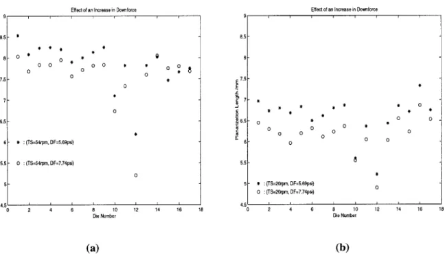
Effect of Change in Table Speed and Down Force on Planarization Length
The planarization lengths of the 15 polished wafers are shown in Tables B. 1 to B.5
of Appendix B. We noticed that the die with the lowest planarization length on each wafer
was the die at the opposite end of the notch, corresponding to die 12 in Figure 3.2. Figures
3.5(a)-(f), which were obtained by taking the average of the planarization lengths of the three repetitions per process condition, shows dies 10 and 12 consistently had the lowest
planarization lengths.
Upon analysis of these figures, the planarization length was found to increase with
force is increased, the polishing pad tends to bend more and conform better to the pattern
density structures and so the planarization length should decrease with down force. When
the table speed is increased, we expect the planarization length to increase as well since at
higher speeds, the pad has less time to flex and conform to different structures as the pad
rotates past different pattern density structures. To verify our findings even further, we
plotted the planarization lengths for scenarios in which there were two changes in process
conditions instead of one; refer to Figures 3.5(e) and 3.5(f).
Effect of an Increase in Downforce
0 2 4 6 8 10 12 14 16
Die Number
18
(a)
Figure 3.5: Effect of a Change in Table Speed
Effect of an Increase in Downforce
5 - .5-7 * * * * .5* 0 * * 0 0 a 0 0 0 0 o-000 0 0 0 .5 -8 5 -* (TS=20rpm, DF=5.69psi) 0 0 (TS=20rpm, DF=7.74psi) 0 2 4 6 8 10 Die Number 12 14 16 18 (b)
and Down Force on Planarization Length
Surface Interpolation of the Planarization Lengths for Different Process Conditions
Figure 3.6 is an interpolated surface of the planarization lengths at different die
positions and the non-uniformity in the planarization length is clear. The planarization
lengths used are the average of three repetitions per process condition. This surface plot
8.5 8 E 7. r 7 %6.5 6 5.5 5 * O * * O 0 0 0 0 0 0 0 00 00 0 0 * (TS=f54rpm, DF=5.69psi) 0 (TS=54rpm, DF=7.74psi) 0 a S E, (D
Effect of an Increase in Table Speed 8.5 8 E 7.5 E c7 .L46.5 6 5.5 5 0 2 4 6 8 10 12 14 16 Die Number (c) 18 1.58 - '.5- 7-'.5 6i.5 5 -0 2 4 6 8 10 12 14 16 Die Number (d)
Effect of a Decrease in Down Force and an Increase in Table Speed
8.5 6 6 5 .5 7 .0 S6.5 a.6 5.5 5
Effect of an Increase in Down Force and Decrease in Table Speed
0 2 4 6 8 10 12 14 16 16 .
DieNumber 2 4 6 8 Die Number10
(e) (f)
depicts the edge effects on planarization lengths and enables interpolation of'
lengths at other die positions where experimental data is unavailable.
Avera2e and Range of Planarization Length for Different Process Conditions
12 14 16
Figure 3.7 shows the planarization lengths that were calculated using the values in
Tables B.2 and B.6. The method of presentation in Figure 3.7 clearly shows that for each 0 00 -0-0 0 0 - * (TS=20rpm, DF=7.74psi) -0 (TS=54rpm, DF=7.74psi) 0 0 0 00 00 0 0 0T=4rm 0 0.9pi ** O * :(TS=20rpm, DF=5.69psi)-0 : TS=54rpm, DF=5.69psi) 18 6.5 .5 .5 5.5 5 4 5 0 00 0 0 0 -0 0 * O * 0 * (TS=37rpm, DF=6.71psi) 0 (TS=54rpm, DF=5.69psi) - -* * ** 0 * 0 0. 000000 00 0 0 0 00 * : (TS=37rpm, DF=6.71psi) 0 0 : (TS=20rpm, DF=7.74psi) 18 planarization
AVG PLEN for:M/M AVG PLEN for:L/L 8000, LO L6000, CL0 - * 4000 100 100Y00 00 0 0 Y -100 -100 X Y -io -100 X AVG PLEN for:H/L
AVG PLEN for:H/H
0 0
Y -100 -100 X AVG PLEN for:L/H
8000- 8000-z z w - 6000- 6000 4000 4000 100 100 100 100 0 0 00 Y -100 -100 X Y -100 -100 X
Figure 3.6: Surface Interpolation of Planarization Lengths (Table Speed/Down Force
levels indicated)
process condition, the planarization length obtained varies somewhat from wafer to wafer.
The vertical lines include the mean, high, and low extracted values for each process
condi-tion, and can be viewed as a measure of statistical variation in the planarization length. For
example, in Figure 3.7c, the planarization lengths obtained for die number 14 ranged from
7.75mm to 8.5mm even though we used the same conditions in our three wafer replicates.
Although we can assume all process conditions are the same for the three repetitions, this
is not exactly true since the pad does not remain in the same condition after polishing.
There is some pad wear as the pad is used to polish more wafers.
z
w
-j
CL
04 02 *N 0 02 N -i *0
(a) Planarization Length for M/M
9000 8500 8000-7500 7000 6500- 6000- 5500- 5000-4500 00 1 2 3 4 5 6 7 8 9 101112131415161718 Die Number
(c) Planarization Length for H/H
90000 8500-8000- T 7500- - 7000-6500 6000- 5500-5000 4500 0 1 2 3 4 5 6 7 8 9 101112131415161718 Die Number
(e)Planarization Length for L/H
9000 8500- 8000- 7500- 7000-6500 -6000 5500 5000-4500 0 1 2 3 4 5 6 7 8 9 101112131415161718 Die Number
(b) Planarization Length for L/L
90000 85008000 -7500 70001 6500 6000-5500 5000 4500 0 1 2 3 4 5 6 7 8 9 101112131415161718 Die Number
(d) Planarization Length for H/L
9000 8500-8000'
}
7500- 7000- 6500- 6000-5500 5000 45006 0 1 2 3 4 5 6 7 8 9 101112131415161718 Die NumberFigure 3.7: Process Condition Summary
M/M => 37 rpm, 6.71 psi H/? => Table Speed = 54 rpm
L/? => Table Speed = 20 rpm ?/H => Down Force = 7.71 psi
?/L => Down Force = 5.69 psi
(e.g. H/H = 54 rpm, 7.71 psi)
Figuie 3.7: Planarization length variation with process conditions
-0
0
* -N
Figure 3.8 provides useful information about how planarization length can be improved. Specifically, increasing table speed or decreasing down force improves pla-narization length. Since the effect is cumulative, both previously mentioned changes would have the best effect when they are both applied to a process. In addition, Figure 3.8
b) shows that variation in table speed is more effective in improving the planarization
length.
Effect of Table Speed and Down Force on Average Planarization Length Effect of Table Speed and Down Force on Average Planarization Length
8000 8000 7800 .5.69p 78005 27600- 276004m 707400 7200 TS .37 rpm DF .71ps 7200 TS -37 n; DF .6.71 psi 7000 7000 6800 - 66800 0-60 -6600 -64 6400 TS -20 pm 6200. 6200-20 25 30 35 40 45 50 55 50*. 6 6.5 7 7.5 8
Table Speed (rpm) Down Force (psi)
(a) (b)
Figure 3.8: Summary of the Effect of Table Speed and Down Force on Average
Planarization Length
Blanket Removal Rates
The planarization length extraction procedure incorporated a blanket removal rate extraction step. Blanket rates typically vary from die to die, and an error in the value of the blanket removal rate can introduce a constant offset between the model prediction and actual oxide thicknesses. The calculated blanket removal rates are shown in Figure 3.9.
(a) 6000 5000 4000 3000 2000 10001 0 1 2 (c) 6000 00 01,5000-4000 3000 2000 1nn
Blanket Rate for M/M
0
'Cu
3 4 5 6 7 8 9 101112131415161718 Die Number
Blanket Rate for H/H 0 0 a 0 0 0 0 Mean: 5371 A/min Std Dev: 279 A/min Range: 1222 A/min
(b) Blanket Rate for L/L 6000 - 5000- 4000-3000 2000 "6000 * 5000 4000 53000-S2000 21000 -2i 34 6 78 9101112134151617 1 2 3 4 5 6 7 8 9 101112131415161718 Die Number
(d) Blanket Rate for H/L
70 1 2 3 4 5 6 7 8 9 101112131415161718 0 1 2 3 4 5 6 7 8 9 101112131415161718
Die Number Die Number
Analysis of Figures 3.9(a) to 3.9(e) shows that the blanket rates are largest under
process conditions of high speed and high down force, and lowest under low speed and
low down force. This agrees with the classical Prestonian CMP model, where "blanket
removal rate" is defined as a quantity which is directly proportional to both pressure (and
thus, down force) and velocity [2].
For the values of down force and table speeds used in this experiment, a few other
observations can be made. It can be seen from the graphs that at lower values of down
force (5.69 psi), increasing the table speed increases the mean blanket rate from 2102 to Mean: 3356 A/min Std Dev: 201 A/min Range: 661 A/min 0 0 0 0 0 0 0 00 00 0 00 Mean: 2102 A/min Std Dev: 137 A/min Range: 496 A/min 0 00 0 0 0 0 Mean: 2655 A/min Std Dev: 265 A/min Range: 699 A/min 0 00 0 0 000 0 0 I I . I . I I I I I ; I . _0
Blanket Rate for L/H
VVV 00 . . . . . . Figu r
Mean: 3308 A/min Average Blanket Rem
5000 Std Dev: 208 A/min Different Process C
Range: 767 A/min
4000 M/M => 37 rpm,
* o H-L/? => Table Speed
3000 * e a o LI? => Table Speed
?/H => Down Force 2000 ?/L => Down Force: (ex. H/H = 54 rpm, 1000 0 1 2 3 4 5 6 7 8 9 101112131415161718 Die Number
Figure 3.9: Blanket rates for different process conditions (e)
2655 A/min (Figures 3.9(b) to 3.9(d)). At higher down force (7.71 psi), it can be seen that
the same increase in table speed causes a much higher increase in the mean blanket rate,
from 3308 to 5371 A/min (Figures 3.9(e) to 3.9(c)). However, higher down force blanket
rates also exhibit larger within-wafer non-uniformity. Note that for the same values of
table speed, a larger value of down force leads to a larger standard deviation and larger
range of blanket rate values. For example, Figures 3.9(b) and 3.9(e) show that for a table
speed of 20 rpm, a low down force gives a range of 496
A
and a standard deviation of137
A,
while a high down force gives a range of 767A
and a standard deviation of 208A.
Thus it is possible to see that an increase in down force will increase the blanket rate, butalso have a negative impact on the uniformity. This trade-off of increasing blanket rate
while decreasing uniformity (and vice versa) is exhibited throughout the data set.
A similar observation can be made for increases in down force. At a lower value of
table speed (20 rpm), an increase in down force results in an increase in mean blanket rate
from 2102 to 3308 A/min (Figures 3.9(b) to 3.9(e)). At the higher table speed of 54 rpm, 0
oval Rate for onditions 6.71 psi = 54 rpm = 20 rpm = 7.71 psi = 5.69 psi 7.71 psi)
the same increase in down force results in an increase in mean blanket rate from 2655 to
5371 A/min (Figures 3.9(d) to 3.9(c)). However, increasing table speed also results in an increase in standard deviation (e.g., 137
A
to 201A
for down force of 5.69 psi) and an increase in range (496 A to 661A
for 5.69 psi).Analysis of Figure 3.8 also confirms that an increase in both table speed and down
force will increase the blanket removal rate while also decreasing the uniformity (Figures
3.9(b), 3.9(a) and 3.9(c)).
The above observations are supported by the summary in Figure 3.10. However, more insight can be gained by further analysis of Figure 3.10. For example Figures 3.10
(a) and (b) show that an increase in either the down force or the table speed has a greater
effect of increasing the mean removal rate at a higher table speed or down force
respec-tively. This is because the slope of both graphs increase with an increase in the down force
in Figure 3.10 (a) and an increase in table speed in Figure 3.10 (b). However, an
examina-tion of Figures 3.10 (c) and (d) show the opposite effect on wafer-level uniformity (as
measured by the standard deviation) in the sense that the slopes decrease with an increase
in table speed and down force.
3.4 Discussion
We know planarization length should vary strongly with pad type, relative speed
and down force. Since the pad type remains relatively the same in our experiments
(ignor-ing pad wear) and the relative speed is the same for symmetric dies, for example dies 10
5500-,-5000 E 11 E 4500 0 (n c4000 - 3500-0 E 030002 030002500 -(a)
Effect of Table Speed and Down Force on Mean Removal Rate
DF -7.71 psi TS .37rpm; DF. 671 psi DF -5.69 psi 20 25 30 35 40 Table Speed (rpm) 45 50 55 5500 ,5000 E E 4500 0 0) S4000 3500 0 " 3000 C 2 2500 9nn 6 6.5 7
Down Force (psi)
(c)
Effect of Table Speed and Down Force on Standard Deviation of Removal Rate
7280- OF .771psi E DF .5.69 psi E 260 0 ~240 220 0200 TS. 37rpm DF. 6.71p o180 C .0 -5160-0 140-6120 20 25 30 35 40 45 50 55 (d)
Effect of Table Speed and Down Force on Standard Deviation of Removal Rate 7280 -TS -54 rpm E 260 -0 C240 220 -TS. 37rpm; DF. 6.71 psi TS .20 rpm 0200. 0 180- -5160- (-140-(120 5.5 6 6.5 7 7.5 8 Table Speed (rpm)
Figure 3.10: Summary of the Effect of Table Speed and Down
Standard Deviation of Removal Rate
Down Force (psi)
Force on the Mean and
a look at Figures 3.5 and 3.7 shows that the planarization lengths for dies 10 and 14 are not
similar. This also applies to dies 12 and 16. This discrepancy prompted an interest in
investigating how well our model in Figure 3.3 performed for dies 12 and 10. Recall that
the extracted planarization length is that which gives the best model fit. Thus large model
(b)
Effect of Table Speed and Down Force on Mean Removal Rate
TS .54 rpm
TS .37 rpm; DF. 6.71 psi TS .20rpm
7.5 8
fit errors could indicate poor estimates for planarization length.
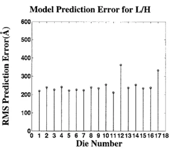
In order to confirm that we do not have significant error in our modeling
methodol-ogy, we have computed the root mean square error for each computation of the
planariza-tion length. An average of the three errors was taken for each process condiplanariza-tion. This is
shown in Figure 3.11.
(a) Model Prediction Error for M/M (b) Model Prediction Error for L/L OUU 500- 400-300 200 100 0 0 1 2 3 4 5 6 7 8 9 101112131415161718 Die Number 04
(c) Model Prediction Error for H/H
U0 500 400 300 200 100 01 2 3 4 5 6 7 8 9 101112131415161718 Die Number
(d) Model Prediction Error for H/L
0 1 2 3 4 5 6 7 8 9 101112131415161718 Die Number 500- 400- 300- 200- 100-0 1 2 3 4 5 6 7 8 9 1100-01112131415161718 Die Number
The plots show that the prediction errors for die 12 are consistently the highest for
04
* 5