Development of the Electronics Architecture for a
Compact Lasercom Fine-Pointing System
by
Grant Gunnison
B.S. Electrical Engineering and Computer Science
Submitted to the Department of Electrical Engineering and Computer
Science
in partial fulfillment of the requirements for the degree of
Master of Engineering in Electrical Engineering and Computer Science
at the
MASSACHUSETTS INSTITUTE OF TECHNOLOGY
September 2020
© Massachusetts Institute of Technology 2020. All rights reserved.
Author . . . .
Department of Electrical Engineering and Computer Science
August 14th
Certified by. . . .
Kerri Cahoy
Associate Professor of Aeronautics and Astronautics
Thesis Supervisor
Accepted by . . . .
Katrina LaCurts
Chair, Master of Engineering Thesis Committee
Development of the Electronics Architecture for a Compact
Lasercom Fine-Pointing System
by
Grant Gunnison
Submitted to the Department of Electrical Engineering and Computer Science on August 14th, in partial fulfillment of the
requirements for the degree of
Master of Engineering in Electrical Engineering and Computer Science
Abstract
CubeSats have become increasingly popular over the past two decades. Since their inception through a collaboration between Cal Poly and Stanford in 1999, CubeSats have allowed researchers and educators worldwide to develop their expertise in the design, assembly, integration and testing of small satellites. Since then, applications for CubeSats have extended beyond the academic and research community into in-dustry and the military. CubeSats bring an unprecedented opportunity for remote sensing due to their relatively low-cost platforms and quick development time. By us-ing Commercial-Off-The-Shelf (COTS) parts and adjustus-ing the scope of their sensus-ing capabilities, CubeSats can be deployed for a small fraction of the cost of traditional satellites. This has led to the development of a large number of CubeSats for ap-plications including: communication systems, weather sensing, Earth imaging and surveillance.
With space being more accessible than ever, the number of CubeSats in orbit has increased dramatically in recent years. With limited access to bandwidth and the growing demand for downlink capacity, engineering teams have looked for solutions beyond RF communication. An alternative communication architecture, laser com-munications (lasercom), is expected to improve performance, using advances in laser beam pointing and tracking technology. In this thesis we describe the electronics ar-chitecture for the Nanosatellite Optical Downlink Experiment (NODE) experiment. This architecture is built on the work of several graduate students and is expected to fly on CLICK-A in late 2020 or early 2021. We present the development of a viable in-tegrated electronics implementation and subsystem laboratory verification for a 1.4U transmit-only CubeSat payload, NODE. NODE will be used to demonstrate down-link capability as part of the CubeSat Laser Infrared Crossdown-link Mission (CLICK)-A research project sponsored by the NASA Science Mission Directorate (NASA SMD). Thesis Supervisor: Kerri Cahoy
Acknowledgments
I would like to express my deepest gratitude to my advisor, Kerri Cahoy for her un-ending support for all her students. Through the endless late nights, early mornings, and even many sleepless nights she has never failed to do everything in her power to support us and for that I will always be in awe and thankful.
I would like to thank NASA Ames for their financial support of me through both the NASA Ames CLICK Mission Award 80NSSC18K1579 and NASA STTR Phase 2 Award 80NSSC18C0211 the past two years to develop CLICK. I would like to thank my department, Anne Hunter and Katrina LaCurts for being understanding during difficult circumstances in my life that forced me to press pause on pursuing my degree and welcoming me back with open arms when I asked to come back.
I would like to thank my friends, close and far, for supporting me through some of the most challenging events I hope to ever need to deal with. If it were not for them, this thesis never would have been written. I would like to thank the CLICK team at MIT for being some of the most delightful and unbelievably smart people I’ve ever gotten to work with, teaching me more than I’d ever hoped to learn and for letting me take part in the adventure. I would like to thank my mom for being supportive of me taking a break from school to help with our difficult family circumstances, fighting for me in every way that she can and never failing to send the best care packages of all time. Finally, I’d like to my dad, I’d be nowhere near the person I am today without the love and support he always gave me.
Contents
1 Introduction 17
1.1 Motivation for CubeSat Optical Communication . . . 17
1.2 Laser Communication Background . . . 19
1.3 NODE Project Overview . . . 21
1.3.1 NODE Background . . . 22
1.3.2 Concept of Operations . . . 24
1.3.3 Revision History . . . 26
1.4 Thesis Objectives and Roadmap . . . 27
2 Approach & Requirements 31 2.1 Revision-2 Testing . . . 31
2.2 REV-3 Design Specifications . . . 34
2.2.1 Bus selection, interface changes . . . 35
2.2.2 Board Requirements . . . 35
2.3 Key Design decisions . . . 38
2.3.1 Bus Communication Design Decision . . . 38
2.3.2 Power Distribution Design Decisions . . . 39
2.3.3 Photodiode board Design Decisions . . . 40
3 Design & Implementation 43 3.1 Bus Communication Interface . . . 43
3.1.1 Component Selection . . . 45
3.2.1 Component Selection & Converter Design . . . 47
3.2.2 Grounding Scheme . . . 52
3.3 Photodiode Board . . . 54
3.3.1 Transimpedance Amplifier Op-Amp Selection . . . 54
3.3.2 Simulation of a TIA using a LTC6268-10 amplifer . . . 58
3.3.3 Implementation of Photodiode Board REV-3.2 . . . 62
4 Results 67 4.1 Power Systems . . . 67
4.1.1 Power Converter Validation . . . 68
4.1.2 Operational Mode Power Consumption . . . 69
4.2 Transmitter Hardware Characterization . . . 70
4.2.1 TEC Controller . . . 72
4.2.2 Laser Diode Bias Controller . . . 74
4.2.3 Photodiode board . . . 75
4.2.4 Temperature sensors . . . 79
5 Conclusion 83 5.1 Summary . . . 83
5.2 Thesis Contributions . . . 85
List of Figures
1-1 Radio and Optical Spectrum Carrier Frequency Comparison. The
spec-trum is shown in a logarithmic scale [9]. . . 20
1-2 Opacity of the Earth’s atmosphere to electromagnetic radiation [50] . 21 1-3 3D model of the NODE payload (REV-2, July 2018 [29] . . . 22
1-4 CLICK A,B & C program demonstration objectives . . . 24
1-5 Concept of CLICK-A operations [26] . . . 25
1-6 NODE Revision-2 Avionics Subsystem Status [19] . . . 27
1-7 CLICK-A Subsystem Requirement Breakdown . . . 28
2-1 NODE Electronics Architecture. Control Signal (COS) . . . 32
2-2 REV-2 Interface Architecture [29] . . . 33
2-3 REV-3 Electronics Architecture . . . 36
2-4 REV-3 Bus Communication Architecture . . . 39
2-5 REV-2 multi-point grounding scheme . . . 41
3-1 REV-3 Bus Communication Architecture . . . 44
3-2 REV-3 Interface Design, February 2020 . . . 46
3-3 -5V Voltage Converter for NODE [48] . . . 51
3-4 Low Noise 300mV Voltage Source, Current Sink . . . 52
3-5 Soft Grounding Scheme for NODE . . . 53
3-6 TIA Diagram including parasitic components . . . 56
3-7 Maximum Achievable Bandwidth for prospective Op-Amps . . . 57
3-8 DC output voltage from input bias current. Lower values are more desirable. . . 58
3-9 TIA REV-3.1 with 13 dB Tap . . . 59 3-10 TIA REV-3.1 with 10 dB Tap . . . 59 3-11 Bode Plot of TIA REV-3.1 with 10 dB Tap . . . 60 3-12 DC2414A Development board for the LTC6268-10 Amplifier [39] . . . 63 3-13 Lab Result from DC2414A Development board using the REV-3.2 design 64 3-14 Simulation result of the REV-3.2 design using the DC2414A
devel-opment board. This is used to compare the result from the physical design on the DC2414A development board. . . 65 3-15 REV-3.2 Photodiode Board . . . 66 3-16 REV-3.2 Single channel Transimpedance Amplifier Design Schematic 66 4-1 Output ripple of TPS6735 -5 V output prior to adding additional
fil-tering. The blue signal shows the voltage ripple output with a 25 mv amplitude. The yellow signal is a voltage measured across a 8.86 Ω resistor in line with the bias current driver to calculate the current ripple. . . 69 4-2 Output ripple of TPS6735 -5 V output after additional filtering is
added. The blue signal shows the voltage ripple output with a 5.5 mV amplitude. The yellow signal is a voltage measured across a 8.86 Ω resistor in line with the bias current driver to calculate the current ripple. . . 70 4-3 Detailed transmitter design block diagram with driver circuits outlined
by the relevant board assignments. [45] . . . 72 4-4 Abbreviated REV-3 TEC Control Circuit. The TEC_SETPOINT
voltage is used to set the temperature of the TOSA cavity by adjusting the voltage across the TOSA thermistor labeled THERM2. . . 74 4-5 Wavelength as a function of cavity temperature, using a set current
bias position. . . 75 4-6 Payload to Bus Interface Pinout . . . 76
4-7 Resulting signal by modulating the TOSA wavelength off of the FBG filter. . . 77 4-8 Comparator output amplitude vs.˜comparator threshold-to-peak input
signal difference . . . 79 4-9 Single Channel Temperature Sensor Circuit . . . 81 4-10 Temperature Sensor Readings using CLICK-A REV-3 Hardware.
Tem-perature values were taken with a Fluke 287 Multimeter. . . 82 5-1 REV-3 model of CLICK-A [29]. . . 86
Acronyms
ADCS Attitude Determination and Control System. 25
BCT Blue Canyon Technologies. 27, 28, 35, 36, 38, 40, 49, 51, 52, 85, 86 BIST Built-In-Self-Test. 32, 34, 40, 79
BJT Bipoler Junction Transistor. 57
CLICK CubeSat Laser Infrared Crosslink Mission. 3, 5, 11, 21, 23, 27–29, 31, 36, 40, 43, 48, 49, 52, 53, 67, 70–72, 77, 79–86
COS Control Signal. 9, 32
COTS Commercial-Off-The-Shelf. 3, 17, 43 CS Chip Select. 45
DAC Digital-to-Analog Converter. 73, 80, 81
DeMi Deformable Mirror Demonstration Mission. 40, 49
ESD Electrostatic Discharge. 32
FBG fiber Bragg grating. 11, 69, 71, 72, 75–78
FCC Federal Communication Commission. 19
FPGA Field Programable Gate Array. 32
FSO Free Space Optical. 22
GBW Gain Bandwidth Product. 41, 55, 56
ISS International Space Station. 24
ITU International Telecommunication Union. 19
KCL Kirchhoff’s Current Law. 55
lasercom laser communications. 3, 19
LEO Low Earth Orbit. 17
LLCD Lunar Laser Communication Demonstration. 22
MEMS micro-electromechanical system. 25, 40 MISO Master Input Slave Output. 45
MOSI Master Output Slave Input. 45
NASA SMD NASA Science Mission Directorate. 3
NIR Near-Infrared. 19, 20
NODE Nanosatellite Optical Downlink Experiment. 3, 17, 21, 23
OPALS Optical PAyload for Lasercomm Science. 22 OSA Optical Spectrum Analyzer. 72, 74
PAT Pointing, Acquisition and Tracking. 22 PCB Printed Circuit Board. 31, 58, 65 PPM Pulse Position Modulation. 25, 79
REV-2 Revision-2. 9, 26–28, 31, 33–35, 38–41, 43, 47, 52, 54, 67, 70, 75, 80, 84, 85 REV-3 Revision-3. 7, 9–11, 26, 28, 34–37, 39–41, 43–47, 52, 54, 58, 67, 70, 71, 74,
75, 80, 82, 84–86 RF Radio Frequency. 17, 21 RPi Raspberry Pi. 44, 45
RTD Resistance Temperature Detector. 33, 80, 81
SNR Signal-to-Noise Ratio. 18
STAR Space Telecommunication Astronomy Radiation. 17
SWaP Size, Weight, and Power. 18, 83
TEC Thermoelectric Cooler. 33, 34, 71–75 TI Texas Instruments. 50
TIA Transimpedance Amplifier. 8, 40, 41, 51, 54, 55, 58, 61, 75–79, 84
TOSA Transmitter Optical Sub-Assembly. 10, 26, 31–34, 40, 54, 62, 68, 69, 71–76, 78, 84
TRL Technology readiness level. 28
Chapter 1
Introduction
In the past two decades small satellite deployments have increased dramatically as ride-sharing opportunities have decreased launch costs. This has opened up opportu-nities for deployment into Low Earth Orbit (LEO) for a broader range of companies and researchers. Traditionally, small satellites have used Radio Frequency (RF) tech-nology to communicate. While developments in RF techtech-nology have improved its ca-pabilities, the RF spectrum is crowded, which constrains the performance of RF com-munications and extends project timelines due to licensing difficulties [1,2]. However, by leveraging Commercial-Off-The-Shelf (COTS) parts from terrestrial free space op-tical communication systems, space based laser communication systems can be de-veloped and deployed at a reasonable cost with more attractive timelines and similar capabilities. The MIT Space Telecommunication Astronomy Radiation (STAR) Lab has set out to demonstrate this with the Nanosatellite Optical Downlink Experiment (NODE). This thesis focuses on the electronics architecture development, design and results for NODE.
1.1
Motivation for CubeSat Optical Communication
With space being more more accessible than ever, the development cycle for deploy-able space systems has shifted dramatically towards smaller and more quickly devel-oped systems. This has allowed larger distributed systems or nets of satellites to be
deployed such as Planet’s Earth imaging project, SpaceX’s StarLink, and OneWeb’s constellation [3,4]. However, these systems have increasing needs for larger bandwidth which is challenging to achieve with RF communication systems. Additionally, these bandwidth constraints are still an issue even for smaller networks or single satellite operations. There is currently no solution that could dramatically relax this com-munications constraint. However, moving to an optical communication system such as NODE could alleviate the bandwidth constraints by operating in a portion of the spectrum that is unregulated.
To understand the Size, Weight, and Power (SWaP) challenge of small satellites, the Friis transmission equation is useful, as shown in Equation 1.1. Generally speak-ing, the more power available to transmit, the higher the data rate will be, as the link capacity depends on the channel bandwidth and Signal-to-Noise Ratio (SNR). However, since we cannot control the channel bandwidth we focus on the SNR, which is a direct derivative of the power received, 𝑃𝑅𝑥.
𝑃𝑅𝑥 ∝
𝑃𝑇 𝑥𝐴𝑇 𝑥𝐴𝑅𝑥
𝜆2𝑅2 (1.1)
As can be seen the Friis formula, 𝑃𝑅𝑥, the power received at the transmitter is proportional to the, 𝑃𝑇 𝑥 power transmitted, 𝐴𝑇 𝑥 transmitter aperture area, 𝐴𝑅𝑥 receiver aperture, 𝜆2 wavelength, and 𝑅2 the distance between the transmitter and receiver. There is little flexibility in the aperture size given the small volume of CubeSats (10-20 cm diameter) and limited budget for a large aperture ground station (2-5 m diameter). There is a fixed amount of transmit power on the CubeSat and the transmit distance is set by the orbit, which depends on the science goals and desire to stay in orbit for the duration of the mission. Therefore the only term that can be meaningfully changed is the 𝜆2, or the carrier frequency. Fortunately, there are roughly 5 orders of magnitude in gain that can be realized by moving into the optical regime and moving the carrier frequency from the S-band (2 to 4 GHz 𝜆 = 15−7.5𝑐𝑚) into infrared spectrum (193 THz 𝜆 = 1550𝑛𝑚), where NODE operates.
CubeSats such as Planet, which is flying X-band transmitters that have theoretical downlinks over 200 Mbps [2]. However, obtaining a license in this band of spectrum is very difficult, and is not practical for CubeSat projects with quick development timelines and limited budgets. In fact, obtaining a license from the Federal Commu-nication Commission (FCC) and International TelecommuCommu-nication Union (ITU) can sometimes take longer than it can take to design, build and test a CubeSat [5,6]. The CubeSat platform would benefit from a high bandwidth communications solution and lasercom can help to fill this gap.
1.2
Laser Communication Background
There are two key benefits to using a laser based communication system over a RF system: better SWaP utilization and available bandwidth. Better SWaP utilization can be seen through the directionality of lasers which is mathematically described in Equation 1.2 and is commonly referred to as the divergence.
𝜃 ≈ 𝜆/𝐷 [7] (1.2)
Due to the reduction in wavelength by moving into the Near-Infrared (NIR) band, the angle of divergence is significantly reduced over an RF system using an aperture of a similar size, D. This allows the energy density of the signal to increase dramatically, which is reflected in the Friis equation and is the main driver of gain over an RF system. Secondly, the reduction in wavelength allows for a reduction in the size of the aperture selected which is advantageous due to the stringent size constraints of CubeSats and can aid in adding additional design latitude.
Another product of moving to a shorter wavelength is the availability of band-width. As can be seen in Figure 1-1 the optical spectrum has carrier frequencies on the order of Terahertz, which makes available more bandwidth than the entirety of the RF spectrum in just a portion of infrared optical spectrum. Beyond the physical limitations due to the SWaP of CubeSats and the transmit channel, the availability of extensive amounts of bandwidth has an unprecedented ability to increase
down-link rates over comparable RF designs. Additionally there is the limited regulation
Figure 1-1: Radio and Optical Spectrum Carrier Frequency Comparison. The spec-trum is shown in a logarithmic scale [9].
from the FCC and ITU in this part of the spectrum currently. They do not require licenses to operate in the NIR spectrum due to the directionality of lasers and low divergence of beams, but only regulate them for eye safety [17]. This reflects the low risk of interference, interception and jamming, a highly attractive feature for military applications [20].
However given all of these benefits, there are drawbacks to using an optical sys-tem over an RF syssys-tem, including: atmospheric turbulence, atmospheric opacity and technical complexity. Atmospheric turbulence can lead to variations in signal inten-sity, phase and direction, meaning that transmission is not always effective through clear air [22]. Additionally, communication is almost never possible through clouds due to scattering. However, these effects can largely be mitigated by having a diverse, numerous set of ground stations. Riesing has shown that having 3 or more diverse locations can provide 90+% downlink availability [23,24,25,27].
Additionally, while there is significant bandwidth available due to the higher car-rier frequencies of lasers, only a portion of that is available for downlinks due to the high atmospheric opacity at infrared wavelengths. Figure 1-2 shows that the Earth’s atmosphere is complete opaque for the majority of the infrared spectrum, but can support transmission at NIR wavelengths, as the atmosphere is comparably transpar-ent to the radio frequency window. Downlinks will be constrained to this portion of
the spectrum, where crosslinks will have the full infrared spectrum available to them. Finally, typical spacecraft pointing abilities are insufficient to meet the pointing requirements of an optical system which requires a secondary, fine pointing, system to be developed [21]. This requires significant technical investment beyond what would be required of a RF system. However, even though it is a more challenging technology to master, the opportunity for an expansion in available bandwidth outstrips the drawbacks of using such a system.
Figure 1-2: Opacity of the Earth’s atmosphere to electromagnetic radiation [50]
1.3
NODE Project Overview
This section will introduce Nanosatellite Optical Downlink Experiment (NODE). It will describe the CubeSat Laser Infrared Crosslink Mission (CLICK) mission, its goals and how those goals will be met through its concept of operation. It will address the previous revisions of the project and the past efforts to develop the project, as well as describe the work that has been completed and will be outlined in this thesis.
Figure 1-3: 3D model of the NODE payload (REV-2, July 2018 [29]
1.3.1
NODE Background
NODE, shown in Figure 1-3, is a proof of concept technology demonstration to show that Free Space Optical (FSO) communications can be done with comparable per-formance to larger scale programs such as Optical PAyload for Lasercomm Science (OPALS) and Lunar Laser Communication Demonstration (LLCD), while in a 3U CubeSat. The work at MIT’s STARLab started with Ryan Kingsbury in 2012 and became his Doctoral thesis in 2015, outlining the system architecture and design. He completed subsystem validation using development boards [26]. Further work was completed by both Riesing and Nguyen in 2015 on the Pointing, Acquisition and Tracking (PAT) subsystem, including simulations of the link conditions and modeled hardware [27,41]. Cierny further developed the optical system required to meet the PAT system requirements in 2017 [42]. Grenfell developed the relative navigation sys-tem to appropriately localize the spacecraft in space on orbit in 2019 [43]. There are many other students that contributed including Christian Haughwout and Rodrigo Diez who made significant contributions to the integrated electronics, Joe Kusters who developed the software and packet architecture and is actively developing the
flight software, Will Kammerer and Derek Barnes who developed and detailed the thermal models and designed the structural payload, Myron Lee who developed the NODE optics and transmitter stabilization algorithm, Caleb Zeigler who developed the downlink channel coding scheme, and Raichelle Aniceto and Alexa Aguilar who evaluated hardware performance in a LEO radiation environment. These publications can be found by year in Table 1.1.
Table 1.1: NODE Contributor Publications
Name Title Year
R. Kingsbury Optical communications for small satellites [26] 2015
K. Riesing Development of a pointing, acquisition, and tracking system for ananosatellite laser communications module [27] 2015 T. Nguyen Laser beacon tracking for free-space optical communicationon small-satellite platforms in low-earth orbit [28] 2015 M. Lee Optomechanical and wavelength alignments of CubeSatlaser communication Systems [13] 2017 O Cierny for the Nanosatellite Optical Downlink Experiment [42]Precision Closed-Loop Laser Pointing System 2017
C. Ziegler A Jam-Resistant CubeSat Communcations Architecture [11] 2017
J. Kusters Laser Communications Using A GPU [16]A Software-Defined Receiver for 2018 A. Aguilar Characterization of commercial step-down converter performancein the low Earth orbit radiation environment [15] 2018
D. Barnes Optomechanical Design, Analysis and Testing of NODE [12] 2018
E. Clements Application to nanosatellite Laser Communications [28]Probabilistic Methods for Systems Engineering with 2018
In 2017, NODE became a part of the CLICK program due to a payload host change due to contract disagreements. The CLICK program is a two mission program A and B/C and therefore NODE will be referred to as CLICK-A through the remainder of this document. Figure 1-4 shows the relative objectives of CLICK-A and CLICK-B/C, where CLICK-A is to demonstrate downlink capabilities and provides a de-risking mission to the CLICK-B/C payloads, which will demonstrate both downlink and crosslink capability. Additionally, the relevant mission requirements used to develop the electronics system for the CLICK-A mission can be seen in Table 1.2.
Figure 1-4: CLICK A,B & C program demonstration objectives Table 1.2: CLICK-A Relevant Requirements
Description Requirement Source
General Size Weight
and Power (SWaP)
<17W Peak Power 1.5U Payload Volume
3U CubeSat
Payload ICD Rev. E PROJ.REQ.23
Mission Lifetime >6 Months MIS.REQ.09
Mission/Operation
Link Duration >10Minutes MIS.REQ.07
Performance Target from 400km to 30cm aperature>10Mbps data downlink MIS.REQ.03 Payload/Bus Interface
Thermal
Management Range 0°to 50° PROJ.REQ.13
Supply Voltages 7-17V PWR.REQ.16
Communication
Protocals SPI & UART Payload ICD Rev. E
1.3.2
Concept of Operations
CLICK-A has been selected for a deployment via the International Space Station (ISS) and its orbit will be at approximately 400 km as shown by the orbital parameters in Table 1.3.2. This will provide approximately a 10 minute transmission window from 20° above the horizon. Prior to reaching the horizon, the payload will wake up and start its boot up sequence, which lasts roughly 45 seconds. Once over the
horizon it will contact the ground station with a low-rate RF link and initiate the Attitude Determination and Control System (ADCS) on the spacecraft to locate the uplink beacon, as shown in in Figure 1-5. Once the uplink beacon is received, the spacecraft’s ADCS will be able to lower its pointing error to less than 2080 urad (1-sigma) at which time the fine-pointing system, using a MEMS FSM will activate to close the loop with an error less than 90 urad (1 sigma) [43]. Once the transmitter and receiver are locked, transmission can be completed.
Table 1.3: ISS Orbital Parameters [19] ISS Orbital Parameters
Orbit Altitude 370-460 km
Orbital Inclination 51.6°
Orbital Velocity 7.6-7.7 km/s (around 27,500 km/h)
Figure 1-5: Concept of CLICK-A operations [26]
CLICK-A utilizes a Pulse Position Modulation (PPM) scheme [10]. PPM orders up to M=128 can be utilized in order to close the link, however it is important to note that the data rate proportionally declines as the PPM order is increased. Nominally, CLICK-A is planning to transmit using 5 ns pulses which could achieve data rates up to 200 Mbps, but depending on the aperture of the ground receiver, such as the planned 30 cm ground station, data rates are likely to be in the 10-50 Mbps range using PPM orders >4 to complete transmission [44]. CLICK-A will also send payload
telemetry data over its RF link to the KSat Lite antenna network at a maximum rate of 1 Mbps. This data will largely include on-board diagnostics, as CLICK-A will only be receiving ground station commands through this link.
1.3.3
Revision History
With the completion of Kingsbury’s PhD thesis in 2015, Revision-1 (REV-1) of NODE’s subsystems were complete. This work included evaluating the design drivers for the ground systems, link budget and payload hardware selections. Through this work a transmitter architecture trade study was completed, which resulted in the avionics system architecture being developed and implemented using development boards [26]. An over-the-air system test was completed in 2017 as well, verifying the functionality of the design. However, many implementation tasks remained af-ter REV-1 was complete, including miniaturization, integration and packaging and designing the appropriate control interfaces.
This work would be followed up by several graduate students that addressed sev-eral aspects of NODE, their publications can be seen in Table 1.1. Specifically re-garding the avionics, two graduate students Rodrigo Diez and Christian Haughwot took the system architecture developed by Kingsbury and used it to develop inte-grated electronics that would fit within the 1.5U payload volume. The result of this and several other graduate student’s work defines Revision-2 (REV-2) for the NODE payload which finished in June, 2018 [29]. As seen in Figure 1-6 REV-2’s avionics system was not completed with the culmination of their work, testing remained to be done on both the Daughter and Transmitter Optical Sub-Assembly (TOSA) boards and the Photodiode board had not begun testing.
With the work completed by several other graduate students, REV-2 was moved from several separate subsystems built out of development boards and benchtop sys-tems, into a integrated payload as shown in Figure 1-3. This payload went through preliminary vibration and Thermal Vacuum (TVAC) testing, but was unable to com-plete functional testing as the avionics systems were not mature.
Figure 1-6: NODE Revision-2 Avionics Subsystem Status [19]
remaining work to complete the integrated electronic systems of REV-2 and is now known as CLICK-A. There is additional work that has been completed in structural, thermal, and optical design, which will be shown in diagrams, but not discussed in detail.
1.4
Thesis Objectives and Roadmap
The objective of this thesis is to address the challenges related to the embedded electronic systems of CLICK-A. The end goal of this research effort has been to ready CLICK-A for deployment. In order to get CLICK-A ready for deployment, numerous challenges needed to be overcome, which are the primary topics of this thesis. These include completing and verifying: board-level designs, inter-board integration, and bus compatibility. The full list of thesis objectives are:
• Test and document the electrical subsystems for REV-2 of CLICK-A.
• Update payload and board specific requirements to meet the functional require-ments for the payload and to integrate with BCT’s bus.
• Design, implement and test new power systems and communication interface for CLICK.
• Simulate, design, implement, test, and characterize a new photodiode board. • Test and characterize the remaining subsystems for REV-3 of CLICK-A. We started by analyzing previous work to understand what the Technology readi-ness level (TRL) of the electronic system was in REV-2. We then imposed new board level specifications to properly integrate existing boards and redesign those that did not meet the new specifications. Finally, given a change in bus provider to Blue Canyon Technologies (BCT), new interface requirements were developed along with a new design that was implemented to be compatible with our bus. Using these revised requirements we addressed the short comings of the current design, and implemented these changes to become Revision-3 (REV-3). These designs were then tested and validated against the new requirements. Figure 1-7 reflects the areas of the payload that will addressed in this thesis, highlighted in light orange, the power and avionics subsystems and their integration into the payload. More specifically, the required redesign of the Photodiode board and bus interfaces will be addressed. Later the payload system integration, testing and validation results of payload’s system will evaluated against the imposed system specifications.
Figure 1-7: CLICK-A Subsystem Requirement Breakdown
This thesis consists of 5 chapters. Chapter 2 addresses the approach taken in completing the design and many of design decisions made for CLICK-A. Chapter
3 addresses the design changes in detail that were made to complete the necessary redesign work as well as the implementation of those changes. Chapter 4 describes testing results at a board and payload level. Finally, Chapter 5 discusses the specific contributions of this thesis and future work that will need to be completed for CLICK-A delivery.
Chapter 2
Approach & Requirements
As a student-led university project, there has been regular staff turnover on CLICK-A. Dozens of students have worked on various portions of the project since 2013, and there have been transitions every year of two. Due to this and hardware component availability over the years, putting together a cohesive and finished system has been a challenge. This chapter will outline the approach used to meet the remaining design requirements to complete CLICK-A in spite of these challenges.
This chapter is outlined in three sections. Section 2.1 outlines the remaining system testing that was completed to finish verification of the REV-2 design. Section 2.2 will outline the updated design specifications needed to integrate the system from an electrical perspective both within the payload and with the bus. Section 2.3 will discuss the key design decisions needed to meet the newly imposed specifications for each board as well as the payload as a whole.
2.1
Revision-2 Testing
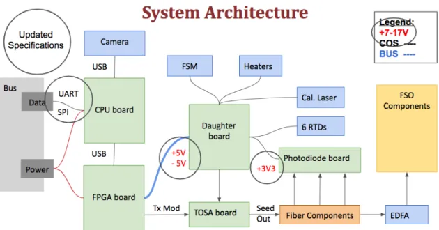
The electronics architecture developed by Kingsbury in 2015 was built using devel-opment boards and and implemented on Printed Circuit Board (PCB)’s by Diez and Haughwot, which can be seen in Figure 2-1 [26].
NODE’s electrical system is made up of 4 main PCB’s that can be seen in Fig-ure 2-1 as well as a Transmitter Optical Sub-Assembly (TOSA) mounting board. In
Figure 2-1: NODE Electronics Architecture. Control Signal (COS)
terms of specific integrated boards, both the CPU and Field Programable Gate Ar-ray (FPGA) boards were developed by Diez [29]. The CPU board is a shield for a Raspberry Pi Compute 3, the payload computer. The shield supports USB interfaces to the bus, beacon camera and the FPGA board. It also provides power conversion for the Raspberry Pi from the bus supply and Electrostatic Discharge (ESD) protec-tion. One of the most important capabilities of the CPU board is to allow the bus to flash the Raspberry Pi on orbit if it gets corrupted. This requires the bus to switch communication from the Raspberry Pi and its peripherals to the bus for reprogram-ming. This need created a complicated scheme on this board, but Diez successfully implemented a system that worked, is shown in 2-2, and described further in Section 3.1.
The FPGA board is an interfacing board between the peripheral devices in the payload and the CPU board. Implemented using the same FPGA that Kingsbury used, the Spartan 6, the FPGA board handles the translation between USB commands from the CPU and SPI for the various drivers on the Daughter board [29]. It also has an RF interface to modulate the Transmitter Optical Sub-Assembly (TOSA), handles the Built-In-Self-Test (BIST) functionality outlined in Kingsbury’s thesis,
and maintains the memory map [13,19]. At the start of the author’s work, the author tested both boards and they have both been electrically validated, including the FPGA’s software defined SPI and UART interfaces.
The remaining three boards: the Daughter, Photodiode, and TOSA boards were developed by Haughwout. The Daughter board houses the electronics for the Ther-moelectric Cooler (TEC) controller, Current Bias Controller, Fast Steering Mirror (FSM) high-voltage driver, calibration laser driver, Resistance Temperature Detector (RTD) circuitry and the interface to the Photodiode board. Functional testing of the Daughter board revealed that the Current Bias controller did not work and without it working, the TEC controller could not be validated. However, the rest of the designs performed appropriately.
The Photodiode board, which provides the circuitry to convert a portion of the TOSA laser output into an electrical signal in REV-2, did not work however. After in-vestigation, the board was designed without enough bandwidth, 200MHz is required, and would not provide enough gain, >10,000 required, in this system. Unfortunately,
the Photodiode board is an integral part of the Built-In-Self-Test (BIST) system, which is used to validate that the transmitter is working properly. In Section 2.3, we discuss the design changes that needed to be made and the driving factors for the required Photodiode board redesign.
The TOSA board is a simple board that acts as a mounting board for the TOSA itself. This is necessary due to the physical constraints in the payload that would not allow for proper heat sinking if the TOSA was mounted to one of the other boards. The TOSA board connects to the Daughterboard for the TEC and Current bias drivers, as well as the FPGA board to receive the modulation signal. Specific attention during layout is needed on this board to keep the modulation signal clean. In going through the REV-2 designs, testing procedures and results were docu-mented for each board. Each board was functionally tested and validated according to the REV-2 implementation, but was not validated to the required features needed for a fully functional payload as these requirements were detailed in a later process. The final specifications and features needed to finish the payload are listed in Section 2.2.
2.2
REV-3 Design Specifications
After functionally testing the REV-2 designs and having the interface design specifi-cations change due to a change in bus provider, a new set of specifispecifi-cations needed to be developed for the payload. The team consistently worked with our bus provider to communicate any specifications that needed to be changed or updated, even if they were a current best estimate. In Table 2.2 the REV-3 specifications can be seen as well as how they compare to the REV-2 specifications. Table 2.2 does not capture all of the requirements for the payload, but highlights the necessary and notable high level changes.
Table 2.1: Updated Payload Specifications. Values in red are driven by the payload. Values in blue are driven from the bus provider.
Specification REV-2 REV-3
Bus Comm. Protocol USB UART, SPI Slave
Supplied Power Rails +5V,+3V3 +7-17V
Peak Power Consumption 10W 17W
Maximum Volume 1U 1.4U
Maximum Mass 0.6 kg 1.5 kg
Min Operational Temp None 0°C
Max Operational Temp None 60°C
2.2.1
Bus selection, interface changes
With a change in prospective bus providers from Planet to BCT and from REV-2 to REV-3, there were several integration challenges that needed to be overcome. Through collaboration with BCT came a slew of different payload requirements in-cluding power distribution, communication protocols, thermal bounds, and updated mass and volume specifications.
While there are several changes that can be seen in Table 2.2 the two most impactful changes from a payload electronics perspective were the power distribution and com-munication protocol requirement changes. The thermal requirements did inform part selection, but did not drive significant changes in hardware design. Figure 2-3 shows the updated communication protocols as well as updated voltage rail requirements to individual boards. The power and communication protocol requirement changes were relatively straightforward; however, due to the in-place architecture of the pay-load, significant changes needed to be made to meet these requirements. Chapter 3 explains the specifics of the designs that were chosen to make the payload compliant with the new bus.
2.2.2
Board Requirements
The requirements shown in Figure 2.2 offer a higher fidelity break down of the func-tional requirements for each board of REV-3. Figure 2.2 does not detail the specifics of the functional requirements, which are detailed in Chapter 3, but rather details
Figure 2-3: REV-3 Electronics Architecture
the input and output specifications that each board must meet. The TOSA board is not listed in Figure 2.2 because it has no active systems on it and is an interfacing board between the TOSA module and the other boards in this system.
As can be seen in Table 2.2 the list of top level requirements for each board is a significant extension over the higher level requirements in Table 2.2; however, this list is not exhaustive and does not detail power consumption, physical layout or EMI requirements.
One of the requirements that was pushed back up to the bus level after going through the requirement analysis and a redesign of the current hardware was the need for current protection. CLICK-A does monitor current for some of its subsys-tems, but not at the aggregate level; however, it does have the ability to slow start its power systems, which ensures that it will not overload the bus power supply at startup. The decision to put current level protection at the bus level involved two parts. First, the needed protection from the payload and BCT’s power system were already capable of providing this functionality. Second, while it was desirable to put additional monitoring into the payload, the project schedule demanded that we push this requirement to the bus and forego additional power system development on the
Table 2.2: Summary of Board Level Requirements for REV-3
Board Requirements
CPU Board • Input Voltage +7-17V
• Differential SPI slave interface to bus • Differential UART interface to bus • USB interface to FPGA board • Selectable USB interface to Camera • Can be reprogrammed & restarted from bus
FPGA Board • Input Voltage +7-17V
• Provide +5 & +3V3 power to Daughter board • USB interface to CPU board
• Modulation interface to TOSA • Heater controller & monitor
• Support interfaces to Daughter Board
Photodiode Board • Input voltage +5V or +3V3 • Input up to 10% of TOSA Power • LVTTL Output
• Input pulse width 5ns • 3 Output Channels
• SPI commanded threshold voltages
Daughter Board • Input voltage +5V and +3V3
• Provide -5V for current bias driver up to 150mA
• TEC controller with selectable temperature • 4x channel 200V FSM Driver
• 6x RTD channels with -20°C - 80°C Range • Calibration laser driver
• EDFA UART interface and mount • Photodiode board interface
payload.
2.3
Key Design decisions
After developing more detailed requirements for the payload on a board by board basis, the REV-2 designs were evaluated to identify where the designs did not meet the requirements. After evaluating the boards, there were three major areas that needed to be addressed: the bus communication design, the power distribution design and the Photodiode board design. In this section, we discuss the approach taken to these key design decisions.
2.3.1
Bus Communication Design Decision
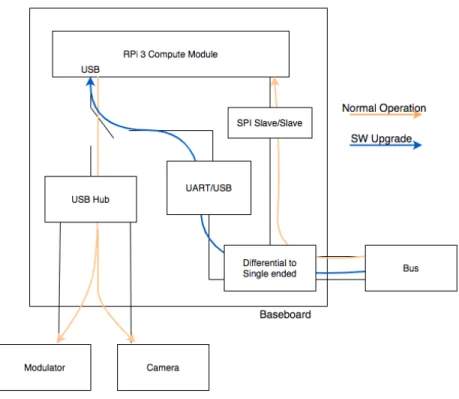
The most significant change required to the payload, due to a change in bus provider from Planet to BCT, is the change to the communication protocol. The original bus from Planet utilized USB to communicate with the payload. This USB would have provided a single high speed bus to communicate over, but unfortunately BCT’s bus could not support a USB interface. Figure 2-4 provides a high level look at the modified bus interface that met the new requirements as shown in Table 2.2.
Fortunately, the payload Raspberry Pi offers several different communication ports natively: USB, SPI, I2C, and UART. Given that BCT supports both UART and SPI, it made sense for us to use them both, SPI for high-speed telemetry, and commanding and UART for reprogramming. However, reprogramming the Raspberry Pi must be done over USB. The Raspberry Pi protocol utilizes USB as it is turned into a mass storage device, so that a new image can be written to it. Reflashing the Raspberry Pi does not need to be a fast operation, we allocated the UART port for this task and would need to provide a converter on the CPU board to turn the UART com-munication lines into USB lines to connect to the Raspberry Pi. The SPI interface would normally be straightforward, directly connecting from the bus to the payload SPI port; however, both the Raspberry Pi and the bus only have SPI masters, which means that we need to put a Slave-to-Slave converter in between the two interfaces so
Figure 2-4: REV-3 Bus Communication Architecture
that they can communicate properly. In Chapter 3, we will outline specifically what the interfaces look like and the design trades we made to arrive at the final design.
2.3.2
Power Distribution Design Decisions
Some key decisions that need to be addressed for the payload power systems include: payload voltage conversion, bus protection, and grounding. The bus voltage require-ment is clear, the payload must be able to handle voltages in the range 7V-17V which creates a straightforward change to the payload. There is concern however, about where to put converters, and how the variable current requirements could impact the payload from a layout perspective. At peak power, 17 W, the payload could require between 1 A to 2.42 A and must be designed to handle the higher current requirement with contingency. In order to manage these concerns, we opted to split the power conversion between both the FPGA and CPU boards and leave the same architecture that existed in the REV-2 design, in place. The CPU board would only provide power
to itself and the camera, where the FPGA board would provide power to itself and the remaining boards and peripherals in the payload as seen in Figure 2-3. In chapter 3 we discuss design specifics, the components we selected, and the trades considered. The payload-bus power interface was updated after lessons learned during the MIT Deformable Mirror Demonstration Mission (DeMi) payload integration with BCT. DeMi’s objective is to demonstrate deformable mirror operation in space to provide wavefront control using a MEMS deformable mirror on a 6U CubeSat. DeMi had a startup concern that would affect the bus power systems due to too much loading capacitance and as CLICK-A is using the same bus, had similar concerns. Fortunately, the converters that were selected for the REV-3 payload provided a slow-start function that could control inrush current to the payload, but did not provide over-current protection, nor did it provide protection to the inrush current created by the bulk capacitance that is placed before the converters. Analysis will follow in Chapter 3 that evaluates the efficacy of moving the current protection to the bus.
Another consideration in integrating with the bus was how to properly ground the payload. At the bus level, BCT implemented a multi single-point reference grounding scheme in compliance with NASA’s Electrical Ground Architecture for Unmanned Spacecraft [46]. REV-2 elected to follow the same grounding scheme on the payload which can be seen in Figure 2-5. However, this architecture did not provide isolation between the power and chassis ground raising concerns about ground loops between boards and the bus. This will be discussed more in chapter 3, but necessitated a design change in REV-3 to a single-point ground return with an isolated power to chassis ground reference.
2.3.3
Photodiode board Design Decisions
As discussed in Section 2.1, the Photodiode board is part of the BIST system that stabilizes the TOSA and validates that the transmitter is working properly. The board houses three parallel Transimpedance Amplifier (TIA) circuits that convert a small amount of optical power from the TOSA into a voltage. While testing the
Figure 2-5: REV-2 multi-point grounding scheme
REV-2 TIA we found that the design did not achieve the necessary performance. This required us to define the appropriate specifications for the board, which are listed in Section 2.3 and redesign the board. These specifications define the amount of input power that is provided to the board, the shape of the input and the required output of the circuit. Given the amount of power being provided from the TOSA, +4-6 dBm, the TIA needs to provide a gain of +75-84 dB to meet the desired output signal. This is a tall order, especially at 200 MHz, to achieve with a TIA. As seen in Equation 2.1, there are three parameters that the designer can control when designing a TIA; however, 𝑅𝑓 is typically defined by the needs of application and both 𝐶𝐼𝑁 and the Gain Bandwidth Product (GBW) are artifacts of the chosen components in the circuit. 𝑓−3𝑑𝑏= √︃ 𝐺𝐵𝑊 2𝜋 * 𝑅𝑓 * (𝐶𝐼𝑁) (2.1) The REV-2 design utilized the OPA657 Op Amp, which provided 46.8 MHz of bandwidth with the desired gain of 20,000. Given our system requirements this performance was insufficient. The part itself has a GBW of 1.6 GHz and a 𝐶𝐼𝑁 of 5.2 pF and in Section 3.3, we discuss the impact of these parameters on the performance of the circuit. We also discuss the design trades and analysis for completing the REV-3 design as well as the considerations taken into account during the layout process to minimize the effect of parasitic capacitance on Photodiode board.
Table 2.3: Summary of Photodiode Board Requirements Photodiode Board Design Constraints
TOSA Output Power +4-6dbm
Optical Splitter Up to 10%
EPM605 Photodiode 0.85A/W
Input Pulse 5ns Square
TIA Gain @ 200MHz
bandwidth Max 20K
Chapter 3
Design & Implementation
In this chapter, we will discuss the specific design of the electrical subsystem for CLICK-A to meet the requirements for REV-3 in Table 2.2. Specific design trades will be discussed, from the subsystem architecture to the component level. Simulation results will be presented to support the design decisions made as well as layout designs as they are relevant.
3.1
Bus Communication Interface
In designing the new bus interface the goal was to preserve the internal payload archi-tecture as much as possible, to reduce development time. In Chapter 2 we discussed the REV-2 design as shown in Figure 2-2 which depicts the interface architecture. It shows a single USB interface and a series of internal switches to allow for the proper data routing. The operational regimes that this architecture supports: regular oper-ation with the CPU communicating to the bus over its SPI interface, communicating with the internal payload peripherals over USB, and a reprogramming regime where the bus would talk directly to the CPU USB interface to load a new image onto the CPU in case of corruption. The reprogramming regime is necessary due to the payload’s use of COTS components in a design with no redundancy for single point failures. Given the operational risk, we opted to include the functionality to repro-gram the CPU given its sensitivity to radiation.
Figure 3-1: REV-3 Bus Communication Architecture
The REV-3 design needed to maintain the reprogramming functionality without the use of a USB interface due to BCT’s bus not supporting the protocol. Given that the payload internally utilized the SPI interface on the Raspberry Pi (RPi), it made sense to directly interface to the bus with a SPI interface. Additionally, since the RPi was required to be reprogrammed through its USB interface, we had to convert that into another protocol that the bus could process. We had our choice between SPI, 12C, and UART and ultimately went with UART due to ease of implementation, low speed requirements, and the breadth of devices capable of providing the protocol exchange.
Figure 3-1 shows the updated block diagram for the REV-3 payload interface. This includes a new block that was not discussed in Section 2.3.1, which is the SPI slave buffer. Both the bus and RPi boards provide a SPI Master interface which required us to provide a bidirectional SPI Slave in-between those devices to make the devices compatible. Additionally, as a deeper understanding of how to reprogram the RPi took shape, the UART to USB block could no longer just be a UART to USB
converter and instead needed to be able to provide custom logic on top of the protocol conversion to successfully reprogram the RPi. This was because we were not able to write the custom logic required on the bus side and therefore had to create a middle man on the payload in between the bus and RPi.
3.1.1
Component Selection
To provide the functionality required for the interfaces, we needed to find compo-nents that could support the differential to single ended conversions, a SPI Slave bi-directional buffer, and the UART to USB conversion. The differential to single ended requirement requires 4 receiver lines 3 for SPI for Master Output Slave Input (MOSI), CLK and Chip Select (CS) and a one for the UART RX line. It also required 2 driver lines for the Master Input Slave Output (MISO) and UART TX lines. Texas Instruments makes a family of parts, the SN65LVDsXX line, specifically for this pur-pose, separated by drivers and receivers. We chose the SN65LVDS33 as a 4-channel receiver and the SN65LVDS9638 a 2 channel driver [32, 33]. These parts can both be seen in the REV-3 implementation in Figure 3-2
To support the SPI bi-directional Slave buffer we needed, there are exactly zero dedicated chips available on the market because SPI is built to support a single mas-ter and multiple slaves on the protocol. We therefore decided to find a MCU with two SPI Slave interfaces that we could write custom firmware for which would also support the UART to USB conversion. The Vinculum-II, from FTDI, provides a so-lution to both the SPI buffer as well as the UART to USB controller. It also supports custom firmware to be loaded on it for our specific application of converting UART to USB with a custom protocol for reprogramming the RPi.
With the final components selected, SN65LVDS9638, SN65LVDS33, and Vinculum-II, the REV-3 interface was implemented and can be seen in the schematic in Figure 3-2. Next, custom drivers needed to be written for both the SPI interface as well as the USB to UART reprogramming interface. The implementation of these drivers is not within of the scope of this thesis.
3.2
Power distribution
When redesigning the power system from REV-2 to REV-3 there were 2 major con-siderations that needed to be evaluated: 1) component selection for power conversion, 2) the grounding scheme and architecturally how to manage current. In order to re-duce schedule impact, we opted to keep the same front end interfacing architecture that NODE had previously used, having main power to connect to both the CPU and FPGA boards. This allowed us to reduce current loops between boards and utilize the excess board area for the additional converters needed to meet the board voltage specifications shown in Table 3.1. Given a peak power input of 17 W and limited space to mount these converters, board area became a significant constraint on the design.
3.2.1
Component Selection & Converter Design
We first defined the voltage rails each board needed to produce along with a conser-vative estimate of the amount of current each line would need to provide. Figure 3.1 shows the outcome of this analysis. If the total power were to be added up, it would be significantly higher than our notated 17 W peak power. This is because the 5V converter on the FPGA board is specified such that both the heaters and the EDFA could be running continuously; however, operationally, this would never happen as the payload will not have to actively heat itself during a transmission. However, if they were activated, the converter should not go down due to over current draw. Additionally, the 1.8V, -5V and 300 mV rails are taken into consideration in the re-maining rails on the CPU and FPGA boards and should be taken out of the total budget. Finally, from the values that were calculated a 25% margin was added on top and without that margin the total consumption is just under 17 W. This analysis is shown in Table 3.2.
We next identified roughly how much space was available on each of the boards and decided that fully integrated switched converters for the high power converters would be necessary on both the CPU and FPGA boards as there was little room
Table 3.1: Summary of Board Level Requirements Power Budge
Board Name Voltages Maximum Required Current
CPU Board 1.8 V 250 mA 3.3 V 1.25 A 5 V .75 A FPGA Board 1.2 V 2 A 3.3 V 1.6 A 5 V 2.5 A Daughter Board -5 V 150 mA Photodiode Board 300 mV 10 mA
Table 3.2: Power Budget Board Rail Specifications
Board Name Voltages Total Power Specification
CPU Board 3.3V 4.13W 5V 3.75W FPGA Board 1.2V 2.4W 3.3V 5.3W 5V 12.5W Heater Subtraction 5V -5.5W
Total Power All 22.55W
Margin reduction 25% 16.91W
for additional magnetics and additional passive components. However for the low power converters, linear regulators and op-amps are used for simplicity. With these specifications set, the next step was to identify converters.
However, before comparing parts online, we consulted the team working on the integrated electronics for CLICK B/C to see if any of the converters that were being used on those boards would also work for CLICK-A. As CLICK B/C is the follow on mission to CLICK-A, it made sense to first validate as many of the components used in CLICK B/C as possible in CLICK-A to help reduce risk. The high power converter, the LTM4622, being used on the flight computer for CLICK B/C was also a good solution for CLICK-A [34]. The LTM4622 provides output and input voltage ranges that match those of CLICK-A, 2 channels per device and comes in a compatible package. This means that CLICK-A only needs 1 converter on the CPU board and
2 on the FPGA board to support all of the high power rails. Further details of the LTM4622 can be seen in Table 3.3.
Table 3.3: LTM4622 Feature Summary [34]
Input Voltage Range 3.6 - 20V
Output Voltage Range 600mV - 5.5V
Output Current 2.5A/Channel
Current Mode Control Yes
Soft-Start 400 𝜇s
Board Area 40 mm2
The LTM4622 met all the requirements for the CLICK-A power converters appli-cation and has some additional useful features. Later, in discussions with BCT there were concerns around inrush current as another project in STAR Lab, DeMi, was correcting issues at startup due to over-current draw as a result of too much loading capacitance [35,36]. The LTM4622 converters provide slow-start functionality that mitigate this risk for all of the components downstream of the converters. However, CLICK-A does have approximately 60 uF of bulk capacitance in front of the convert-ers and the bus would need to be able to handle the inrush current created by this capacitance without shutting the payload down by reaching the agreed upon 3.7 A current limit. BCT was able to later verify through simulation that the 3.7 A current limit would not be reached, as the inrush current to CLICK-A would not exceed 700 mA due to this exposed bulk capacitance. We next moved on to component selection for the low power converters.
There are 3 low power converters that we selected for CLICK-A, the 1.8 V con-verter for the CPU, the -5 V concon-verter for the Daughterboard, and the 300 mV converter for the photodiode board. The 1.8 V converter was chosen to be a linear regulator due to its low power requirements and simple application. The LM1117 was considered, as it only required 2 external components, an input and output sta-bilization capacitor. However, one potential concern with this part was that it could burn up too much unnecessary power, as linear regulators are inefficient. Equation 3.1 shows the efficiency for this device, where 𝐼𝐼𝑁 can be assumed to match 𝐼𝑂𝑈 𝑇 because 𝐼𝑂𝑈 𝑇 >> 𝐼𝐶𝐶, where 𝐼𝐶𝐶 is the current consumed by the device, which in
this case is 5 mA or 2% of the maximum specified current draw. Efficiency = 𝑉𝑂𝑈 𝑇 · 𝐼𝑂𝑈 𝑇
𝑉𝐼𝑁 · 𝐼𝐼𝑁
(3.1) This leaves the LM1117 with an efficiency of 55%, which is not great, but accept-able for this application given its low power consumption. To make sure the device did not require any additional heat sinking while running at maximum load, the junction-to-ambient thermal resistance is calculated in Equation 3.2. The junction to ambient thermal resistance needs to be ≥ 136°/W to forgo additional heat sinking. The value calculated, using the maximum ambient temperature of 60°C, as the upper operational temperature bound, comes out to 173.3°/W confirming there is no need for an additional heat sink.
𝜃𝑗𝑎= (𝑇𝐽(𝑚𝑎𝑥) − 𝑇𝐴(𝑚𝑎𝑥))/𝑃𝐷 (3.2)
𝑃𝐷 = (𝑉𝐼𝑁− 𝑉𝑂𝑈 𝑇) * 𝐼𝑂𝑈 𝑇 (3.3)
The next power converter, for the -5 V rail, needs to provide about 750 mW of peak power, which requirs a switching converter, given the inverted rail voltage and the amount of power being delivered. There were several choices given the different converter topologies that can provide a negative voltage, such as a switched capaci-tor, inverted buck-boost or a Cuk converter. However, given that the Cuk topology requires 2 inductors instead of 1 for the inverted buck-boost, that topology was elimi-nated due to board space constraints. Taking a look at a couple of the chips available for the other topologies yielded potential solutions such as Texas Instruments (TI)’s LM2662, TPS6735 and Maxim’s MAX735. The LM2662 would have been a fine choice, but requires a 20 kHz or 150 kHz oscillator, which tend to be bulky due to their low frequency. So the LM2662 was eliminated. The remaining two converters utilized the same inverted buck-boost topology and as such are almost indistinguish-able as they have the same efficiency, input voltage range, peak current drive, and operational temperate range [37, 38]. In fact, these devices are even pin for pin
com-Figure 3-3: -5V Voltage Converter for NODE [48]
patible and can be swapped out for each other. The TPS6735 was selected because it is about 60% of the cost of the MAX735, but either chip would work just fine. The topology of the converter can be seen in Figure 3-3.
The final converter to be specified was the 300 mV converter used on the Photodi-ode board to create a higher virtual ground in the TIA circuit as explained in Section 3.3. This converter needed to be a low noise, current-sinking device. Unfortunately, linear regulators are not built to sink current. As a switching converter would be overkill for this application, we opted to build a reference ourselves using an op-amp that could sink the sufficient current. It was not necessary for this voltage to be highly accurate, but it was important for it to be as stable and low-noise as possible. Fortunately, there are a number of low-noise op-amps available that could be used for this design. Figure 3-4 shows the layout designed for this voltage reference, using a low-noise op-amp, the LTC6258, in a voltage-follower configuration. The LTC6258 is settable by two in-series resistors with ±2% accuracy using 1% resistors. It is stable over the 60°C operational temperature range to 0.6%, which is largely driven by the 25ppm/K temperature coefficient for the resistors in the voltage divider and has less than 0.1%𝑉𝑝−𝑝 noise.
With each of these designs completed and simulated for performance, the designs were moved into the board layout phase and the work turned towards making sure the design was compliant with the grounding scheme used by BCT at the bus level.
Figure 3-4: Low Noise 300mV Voltage Source, Current Sink
3.2.2
Grounding Scheme
As noted in Section 2.3.2, there were concerns about the grounding scheme of CLICK-A that needed to be taken into consideration. BCT’s bus implemented a multi single-point grounding system which provides a chassis ground reference to several devices within the system as the single-point ground reference. With this architecture, it is possible for current loops to be created if there is insufficient isolation between the power and chassis ground. When REV-2 of CLICK-A was designed, isolation was not provided between boards nor was it provided between chassis and power ground. This lack of isolation allows for potential power return paths through the chassis con-nections. While having current return through the chassis is unlikely to directly cause issues at DC, the potential for high frequency noise to be coupled through ground loops can be reason for concern. Each of the ground loops has the potential to both generate and receive electromagnetic energy. To try to stay compliant with NASA’s standard for grounding unmanned spacecraft our team redesigned the grounding plan for REV-3 of CLICK-A [20].
Given how CLICK-A is planned to be physically integrated into the bus, by di-rectly bolting its chassis to the bus, there were two options for properly grounding the payload’s electronics. One option is to provide isolation through a physical resistance
Figure 3-5: Soft Grounding Scheme for NODE
in the electronics that would separate CLICK’s power ground from the chassis ground. This approach is “called soft grounding”. An implementation of soft grounding can be seen in Figure 3-5 where the standard recommendation for isolation on a power bus is a modest 2 kΩ impedance between the chassis and power ground with no more than 0.1 𝜇F of capacitance across the payload. As can be seen in Figure 3-5 this requires a resistor to be placed at the chassis ground on the electronics. Since CLICK-A has 5 boards in its system, none are connected to chassis directly, and all are connected to the same power ground, only a single resistor is needed to create this isolation. The configuration shown in Figure 3-5 limits the number of extra components needed to achieve isolation and provides the desired isolation between the chassis and power ground.
The second option is to disconnect the power ground from the chassis ground and have no chassis connection to the electronics on CLICK-A. This provides per-fect isolation between the payload and the chassis ground, eliminating the possible chassis power return and high frequency ground loop issues that could have arisen. However, this does introduce a concern that the body of the spacecraft could be at a significantly different potential than the electronics and could introduce an unin-tended failure mode by having something accidentally connect the power ground of a board to the body of the payload. This could be a single path failure mode for the mission and is generally avoided due to its potential downsides. Additionally, it has potential to introduce common mode noise to the board systems, which is concerning for CLICK-A’s analog systems.
After exploring each option with BCT, the first option was chosen to help elimi-nate the risk of the potential failure mode and the risk of additional common mode voltages on NODE’s electronics.
3.3
Photodiode Board
When redesigning the Photodiode board from REV-2 to REV-3, care had to be taken with regard to the constraints laid out in Section 2.3.3. Given that there were two degrees of freedom, optical tap percentage and transimpedance gain, we considered how much room there was to operate within these constraints and which parameters would be able to produce valid designs. We evaluated the optical splitters shown in Table 3.4. Given that the TOSA has a tunable output power, it was important to assume that the TOSA is operating at its maximum power so that the TIA could be designed not to saturate, and so that there would be sufficient power further down the optical chain. The analysis is done using a +6 dBm output from the TOSA, assuming that any losses due to misalignment in splices would result in a decreased output voltage swing or reduce any bandwidth margin available. Given our desire for high output voltage swing, 3 V Pk-PK, we analyzed three possible splitters based on their possible tap values, how much power each would deliver to the photodiode, and in turn what the maximum possible output voltage swing would be. A maximum gain parameter was chosen after evaluating a few different TIA amplifiers and finding 20 K to be a practical value based on the 200 MHz of bandwidth required as shown in Table 2.3, but would need to revisited during simulations. As can be seen in Figure 3.4, the 20 dB splitter provided insufficient optical power to achieve the desired output swing of 3 V.
3.3.1
Transimpedance Amplifier Op-Amp Selection
To meet the functional requirements for the TIA as shown in Table 2.3, an initial component search identified 4 potential amplifiers that would be suitable to this application. Amplifiers were evaluated based on parameters shown in Table 3.5,
Table 3.4: Summary of Board Level Requirements Optical Splitter Choices
TOSA Output Power +4-6dbm +4-6dbm +4-6dbm
Optical Tap − 10dB 13dB 20dB
Photodiode Input = -4dbm -7dbm -14dbm
Photodiode Responsivity * .85A/W .85A/W .85A/W
Photodiode Output Current = 338𝜇𝐴 170𝜇𝐴 33.8𝜇𝐴
Maximum Gain * 20K 20K 20K
Peak Output = 6.76V 3.4V 676mV
Table 3.5: Amplifier Design Parameters TIA Amplifier Choices
Device Name OPA858 OPA855 LHM6629 LTC6268-10
Gain Bandwidth (GHz) 5.5 8 4 4
Slew Rate (V/𝜇𝑠) 2000 2750 1600 1500
Input Capacitance 0.8pF 0.8pF 2.1pf 0.55pF
Output Swing 1.3V 1.3V 1.7V 3V
GBW, slew rate, input capacitance and output swing.
The first amplifier parameter evaluated was the slew rate of the amplifiers using Equation 3.4, making sure that the slowest of them, the LTC6268-10, was capable of providing its full voltage swing, given a 5 ns pulse. All of the amplifiers were able reach their maximum swing voltage within half of the pulse time with healthy margin.
𝑆𝑙𝑒𝑤_𝑟𝑎𝑡𝑒 · 2.5 ns > 3𝑉 (3.4)
The second parameter evaluated was the maximum achievable bandwidth which incorporates several different parameters. In order to calculate this value, the transfer equation needed to be derived for the TIA circuit with all of the parasitic capacitances. The TIA circuit can be seen in Figure 3-6, and by using Kirchhoff’s Current Law (KCL) the transfer equation can be derived. With some manipulation, the transfer function can be put into the form seen in Equation 3.5. This form is useful because by modeling the response of the TIA as a Butterworth response, a maximally flat response filter, the maximum available 𝑓−3𝑑𝐵 bandwidth can be found by setting the value of Q = √2 [47]. The equation for Q, the damping component of the response,
Figure 3-6: TIA Diagram including parasitic components
can be found in Equation 3.6, where 𝜔𝐴 is the maximum achievable bandwidth. 𝑉𝑂 𝐼𝐷 = 𝑅𝐹 · 𝐴𝑜𝑙 𝐴𝑜𝑙+ 1 · 𝜔 2 𝑜 𝑠2+ 𝑠 · 𝜔𝑜 𝑄 + 𝜔 2 𝑜 (3.5) 𝑄 = √︁ (𝐴𝑜𝑙+1)·𝜔𝐴 𝑅𝐹·(𝐶𝑆+𝐶𝐹) 𝜔𝐴· (1 + 𝐴𝑜𝑙· 𝐶𝐶𝐹 𝑆+𝐶𝐹) + 1 𝑅𝐹·(𝐶𝑆+𝐶𝐹) (3.6) Fortunately, by applying an approximation, such as 𝐶𝑆 >> 𝐶𝐹 and noting that GBW = 𝜔𝐴 · 𝐴𝑜𝑙, a simpler formula can be used to calculate the the maximum available 𝑓−3𝑑𝐵 bandwidth. This is possible because we can say that 𝐹𝑜 is the same point as Q when Q =√2using a Butterworth model of the maximum available 𝑓−3𝑑𝐵 bandwidth of the response.
𝐺𝐵𝑊 = 2𝜋 * 𝐹𝑂 −3𝑑𝐵2 · 𝑅𝐹𝐶𝑆 (3.7)
Using Equation 3.7, we can plot the maximum 𝑓−3𝑑𝐵 bandwidth possible for each of the op-amps across a range of transimpedance gains, which is shown in Figure
![Figure 1-1: Radio and Optical Spectrum Carrier Frequency Comparison. The spec- spec-trum is shown in a logarithmic scale [9].](https://thumb-eu.123doks.com/thumbv2/123doknet/14744384.577661/20.918.223.699.168.366/figure-radio-optical-spectrum-carrier-frequency-comparison-logarithmic.webp)
![Figure 1-2: Opacity of the Earth’s atmosphere to electromagnetic radiation [50]](https://thumb-eu.123doks.com/thumbv2/123doknet/14744384.577661/21.918.223.699.380.686/figure-opacity-earth-s-atmosphere-electromagnetic-radiation.webp)
![Figure 1-3: 3D model of the NODE payload (REV-2, July 2018 [29]](https://thumb-eu.123doks.com/thumbv2/123doknet/14744384.577661/22.918.266.653.108.476/figure-d-model-node-payload-rev-july.webp)
![Figure 1-6: NODE Revision-2 Avionics Subsystem Status [19]](https://thumb-eu.123doks.com/thumbv2/123doknet/14744384.577661/27.918.261.669.130.415/figure-node-revision-avionics-subsystem-status.webp)

![Figure 2-2: REV-2 Interface Architecture [29]](https://thumb-eu.123doks.com/thumbv2/123doknet/14744384.577661/33.918.225.691.639.1037/figure-rev-interface-architecture.webp)