HAL Id: hal-01961179
https://hal.insa-toulouse.fr/hal-01961179
Submitted on 16 May 2019HAL is a multi-disciplinary open access
archive for the deposit and dissemination of sci-entific research documents, whether they are pub-lished or not. The documents may come from teaching and research institutions in France or abroad, or from public or private research centers.
L’archive ouverte pluridisciplinaire HAL, est destinée au dépôt et à la diffusion de documents scientifiques de niveau recherche, publiés ou non, émanant des établissements d’enseignement et de recherche français ou étrangers, des laboratoires publics ou privés.
Polymorphism of Two-Dimensional Halogen Bonded
Supramolecular Networks on a Graphene/Iridium(111)
Surface
Muriel Sicot, Damien Tristant, I.C. Gerber, Bertrand Kierren, Frederic
Cherioux, Yannick Fagot-Revurat, Luc Moreau, Julien Granet, Daniel
Malterre
To cite this version:
Muriel Sicot, Damien Tristant, I.C. Gerber, Bertrand Kierren, Frederic Cherioux, et al.. Polymor-phism of Two-Dimensional Halogen Bonded Supramolecular Networks on a Graphene/Iridium(111) Surface. Journal of Physical Chemistry C, American Chemical Society, 2017, 121 (4), pp.2201–2210. �10.1021/acs.jpcc.6b09892�. �hal-01961179�
Polymorphism of 2D Halogen Bonded
Supramolecular Networks on a
Graphene/Iridium(111) Surface
Muriel Sicot,
∗,†Damien Tristant,
‡,¶Iann C. Gerber,
‡Bertrand Kierren,
†Fr´
ed´
eric
Ch´
erioux,
§Yannick Fagot-Revurat,
†Luc Moreau,
†Julien Granet,
†and Daniel
Malterre
††Institut Jean Lamour, UMR 7198, CNRS Universit´e de Lorraine, BP 70239, 54506 Vandoeuvre l`es Nancy,France
‡Universit´e de Toulouse, INSA-CNRS-UPS, LPCNO, 135 Avenue de Rangueil, 31077 Toulouse, France
¶CEMES, UPR 8011, CNRS-Universit´e de Toulouse, 29 rue Jeanne Marvig, BP 94347, 31055 Toulouse, France
§Institut FEMTO-ST, Universit de Bourgogne Franche Comt´e,CNRS,15B Avenue des Montboucons, F-25030 Besan¸con cedex, France
E-mail: muriel.sicot@univ-lorraine.fr
Abstract
The properties of 2D supramolecular self-assemblies on surfaces depend on the fine balance between molecule-substrate and molecule-molecule interactions. In this ar-ticle, we study the growth of 1,3,5-tri(4’-bromophenyl)benzene (TBB) monolayer on graphene epitaxially grown on Ir(111) by means of low temperature scanning
tun-description of the molecules in interaction with the Gr/Ir(111) substrate, using density functional theory (DFT). In order to figure out the impact of the underlying metal-lic layer upon the self-assembling behavior of the molecules and their properties, we compare our results with those theoretically obtained on pristine graphene or experi-mentally achieved on HOPG. We demonstrated that the use of the Ir layer allows the formation of large extended, continuous and two-dimensional supramolecular networks laying even over Ir step edges like a carpet. In addition, we highlighted the obtention of two structural polymorphs never observed on HOPG. In the light of DFT simula-tions, we assumed that the formation of these polymorphs is driven by the balance between molecule-molecule interactions, due to Halogen bonds (XB), and the tailored molecule-surface interactions due to the presence of Ir layer.
Introduction
Molecular self-assembly is the spontaneous association of molecules into structurally stable
well-defined aggregates joined by noncovalent interactions. This key concept allows for the
engineering of molecular architectures with novel or targeted optical, electrical and magnetic
properties. In supramolecular assembly, molecular building blocks are interconnected to
each other by virtue of directional intermolecular interactions such as halogen bonding,1
hydrogen bonding,2,3 dipolar coupling,4,5 metal coordination,6–8 van der Waals forces9–11
or π-π interactions.12 Nevertheless, on a surface, the resulting molecular geometry does
not depend only on intermolecular interactions but on a subtle balance between
molecule-molecule and molecule-molecule-substrate interactions. Therefore, opting for the right combination
composed of a molecular building unit and a substrate would lead to the desired functional
nanomaterial. Moreover, tunability could be obtained by the subtle modifications of the
substrate properties.
In this framework, epitaxial graphene on metal (Gr/M) has emerged as an appealing
sup-port for molecular self-assembly.13First, the presence of a moir´e nanopattern14–17originating
ad-sorption energy landscape that can be exploited to grow novel molecular architectures such
as nanoporous18or Kagom´e networks19that could not be achieved using HOPG20,21 or other
substrates. In addition, the coupling between Gr and the metal is an extra parameter to
play with in order to modify the molecule-substrate interaction and therefore to obtain
vari-ous and original molecular arrangements. For example, the growth of iron-phthlocyanine on
Gr/Ru for which the carbon-metal interaction is strong leads to a Kagom´e lattice whereas
same molecules form densely packed 2D islands on Gr/Pt for which the coupling is weak.22
Moreover, the advantage of using Gr/M substrates relies on the fact that even more
complex Gr/X/M interfaces can be built for fine adsorption tuning by means of controlled
intercalation of a foreign species X (atoms or molecules) between the graphene layer and the
metallic support.23–30 Once again, the primary objective behind this interface engineering is
to finely tune the electronic properties of the topmost graphene layer in order to have control
on the resulting molecule-substrate interaction. In this vein, the possibility to manipulate
molecular adsorption at the nanometer scale and to tailor molecular self-assembly using
in-tercalation has been recently demonstrated.31,32 Finally, the growth of epitaxial graphene
is carpet-like such that the carbon layer continuously covers the metallic step edges.29,33,34
Hence, unlike any other substrate, one could expect to avoid the disruption of the
molecu-lar network and therefore, obtain low-defect interface for graphene-based organic electronic
devices with high performances.
Although HOPG has been widely used for molecular self-assembly, there is no
straight-forward way to deduce from these existing studies the self-assembly behavior on Gr/M since
the interaction of graphene with the underlying layers (carbon in the case of HOPG and
metal in the case of Gr/M) plays an important role in the number and nature of phases even
in the case of weakly coupled Gr/M interfaces.20–22,35 Therefore, in order to understand how
molecular properties can be affected by the substrate, it is crucial to determine the impact
of the underlying metal layer below graphene on the self-assembly.
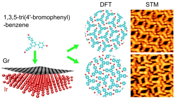
properties of self-assembly of 1,3,5-tri(4’-bromophenyl)benzene (TBB) molecules on Gr/Ir(111).
The particular choice of this molecule is motivated by the fact that it can form self-assembly
driven by halogen· · · halogen bonding on various substrates.36–38 Moreover, halogen bonded
molecular self-assembly on Gr/M substrates are lacking. As this molecule has been
previ-ously investigated on semi-conducting,39 metallic37,40–42 or graphite (HOPG) substrates,37
a direct comparison with our results allows us to elucidate the role of the Gr/Ir interface
in the assembly process. In this work, we demonstrate by LT-STM, the formation of a
supramolecular carpet of high structural quality on Gr/Ir. In addition, the coexistence of
two polymorphs is observed. We show that the two phases are composed of TBB dimers
stabilized by Br· · · Br and Br· · · H bonds. The two polymorphs have been determined to be
different than the single one previously obtained on HOPG37 revealing the crucial role of
the layer lying under the topmost graphene sheet. DFT demonstrates that the Ir has only
little influence on the adsorption geometry of the molecule. However, LT-STS and simulated
PDOS reveal that Ir acts on the energies of the HOMO and LUMO states of the adsorbed
molecule via charge transfer with graphene. Finally, the comparison of our results with
previous works shows that the use of Gr/Ir(111) results in original packings with unique
electronic properties.
Results and discussion
System
The substrate is made of one single monolayer of graphene epitaxially grown on Ir(111) and
prepared as described elsewhere.30 At the sample scale (about one square centimeter),
low-energy electron diffraction (LEED) patterns (not shown here) reveal a long-range ordered
and single-domain graphene overlayer. A moir´e superstructure resulting from a mismatch
between graphene and Ir(111) lattices is also observed both with LEED and scanning
to approximately 10 times of the lattice constant of graphene and 9 times that of Ir(111).
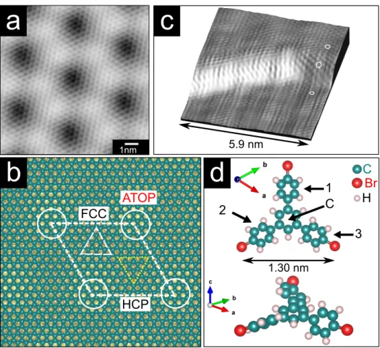
This is in good agreement with earlier works.15 As shown in Fig.1(b), this graphene
cor-rugation is responsible for the creation of three regions for possible preferential molecular
adsorption: FCC-, HCP-and ATOP-type. They are named for whether the center of the
carbon hexagons sites above an Ir fcc-, hcp-hollow or atop site (up triangle, down triangle
and circles circumscribe these regions in Fig. 1(b)). Fig. 1(c) displays a high-resolution
STM topograph showing the graphene overlayer that spreads across an Ir step without
visi-ble defect at the atomic scale. This carpet-like growth has already been described by Coraux
et al.33As we will show later on, this particular structural property is a key feature to obtain
low defect density 2D self-assembled molecular networks (SAMNs). Indeed, this property
to cover the Ir edge might lead to a reduction of the Ehrlich-Schw¨obel barrier and therefore
promote step edge crossing of the molecules during diffusion in comparison with diffusion
on uncovered metallic surfaces such as Ag, Au. The TBB molecule is star shaped (Fig.
1(d)) and possesses a bromophenyl group at the extremity of its arms. In the gas-phase, a
single molecule is not flat : each arm is rotated by a dihedral angle δ of about 39◦ between
the phenyl groups and the central ring as obtained by gas-phase DFT optimization of the
a
c
1nm 5.9 nm ATOP 1C 2 3d
b
FCC HCP C Br H 1.30 nmFigure 1: (a) Atomically-resolved STM topograph of the moir´e structure of the graphene layer on Ir(111) (UT = 0.15 V; IT = 2 nA). (b) Schematic illustration of the DFT optimized
C(10 × 10)/Ir(9 × 9) unit cell. Carbon and Ir atoms are represented as green and yel-low spheres respectively. The dashed white rhombus outlines the supercell of the moir´e superstructure with three different regions marked by a full circle (ATOP), an dashed up-pointing triangle (FCC) and a dotted down-up-pointing triangle (HCP) (see text). (c) 3D rendering of an atomically-resolved STM topograph showing the continuity of the graphene film across an Ir step edge. Three white hexagons schematically represent sp2 bonds of the
graphene film adsorbed on the upper, lower terraces and on the Ir step edge. (17 × 11 nm2, UT = 9 mV; IT= 12 nA). (d) ball-and-stick model of the 1,3,5-tri(4’-bromophenyl)benzene
(TBB) molecule in gaseous phase. Top: top view showing the three bromophenyl arms labeled 1,2 and 3 and the central benzene ring labeled C. Bottom: side view showing the dihedral rotation of the side groups.
Growth
The growth of TBB on Gr/Ir has been investigated in the submonolayer range. At early
shown in Fig. 2(a). At increasing coverages, TBB molecules self-assemble starting from the
Gr/Ir step edges and form one molecule thick nanoislands as pointed by a white arrow in
Fig. 2(b). Large defects on terraces can anchor molecules and act as starting points for
molecules to self-assemble as well. Fig. 2(c) displays an STM topograph of a 2D SAMN of
TBB molecules that spontaneously formed at higher coverage. Molecular patches as large
as 200 nm were observed by means of STM. Two different polymorphs, labeled 2MOL and
4MOL in the following, were identified (Fig. 2(c) and (d)). Their respective occurence and
molecular packing will be discussed in details later in the text. White parallel lines in Fig.
2(c) outline one main crystallographic direction of the first polymorph. Those lines are not
deviated when crossing the Gr/Ir step edge displayed as a vertical black line according to
the color scale in the center of the STM image. This shows the continuity of the SAMN over
the step edge. This feature can be easily understood considering the carpet-like growth of
the graphene film on Ir as mentioned earlier: molecules adsorbed at any places on graphene
independently of the vertical graphene lattice bending caused by the presence of Ir step
edge. This feature is also well illustrated for the second polymorph in the 3D rendering of
an STM topograph in Fig. 2(d) where the molecular network smoothly adopts the graphene
a
5 nmb
d
low highc
2 nm 5 nmFigure 2: Early stage of growth of TBB on Gr/Ir(111). STM topographs recorded after deposition of (a) 0.05 monolayer (ML) and (b) 0.2 ML of TBB. The white arrow in (b) points at a self-assembled nanoisland. (c) STM topograph of 1ML-thick nanoisland of molecules organized in the 4MOL phase. White dashed lines highlight the continuity of the molecular lattice across the Gr/Ir step edge. (d) 3D rendering of an STM topograph recorded on a 1ML-thick molecular nanoisland of the 2MOL phase. Blue and green rhombuses in (c) and (d) outline the unit cells of the 4MOL and 2MOL phases respectively. Parameters are: (a) (65 × 59 nm2, U
T = 2.22 V; IT = 20 pA), (b) (70 × 56 nm2,UT = 2.22 V; IT = 40 pA), (c)
(17 × 11 nm2,U
T = 2.22 V; IT = 0.25 nA) and (d) (10 × 10 nm2,UT = 2.22 V; IT= 0.09 nA).
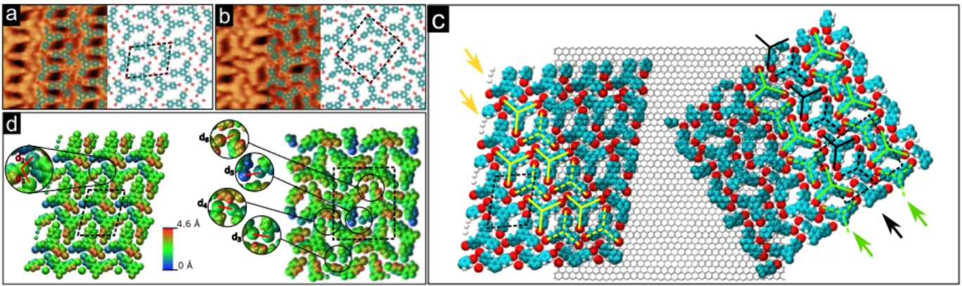
Molecular packings
In the next paragraph, we will discuss the occurence and the molecular packing of the two
TBB polymorphs on graphene. For each polymorph, three different domains rotated from
another by 120◦ are observed, in good accordance with the underlying 3-fold symmetry of
the graphene lattice. The two phases are formed in extended domains in the surface together
with nanoislands composed of the two coexisting phases as shown in Fig. 3(a). On this STM
topograph, the two polymorphs are visible and form three domains separated by two domain
boundaries highlighted with dashed lines.
Submolecular resolution allowed us to identified adsorbed molecules as intact TBB molecules
since under specific tunneling conditions such as in Fig. 3(a) and Fig. 4(a,b): carbon rings
clearly visible.
As a consequence, a simple ball and stick model of the molecule can be laid over the STM
image of Fig. 3(a). One can readily notice that the building block of the supramolecular
network is a molecular dimer as schematically drawn in Fig. 3(b). We will show in the
following that dimers are stabilized with C-Br· · · Br and Br· · · H bonds. This dimer can be
characterized by the distance between the two central carbon rings C (Fig. 1(d)) together
with the relative angle between the γ directions made by opposite bromophenyl arms. The
unit cells shown in Fig. 3(a) of the 2MOL (green full line) and 4MOL (blue dashed line)
phases host two and four TBB molecules respectively. The two phases are oriented such that
the diagonal of the 2MOL unit cell corresponds to the shortest side of the 4MOL unit cell.
The determination of the orientation of the supramolecular network with respect to
the substrate was not possible neither from LEED patterns nor STM topographs. Indeed,
molecules are damaged under the electron beam probably due to electron-induced
dissocia-tion. Moreover, the set of tunneling parameters (IT, UT) needed to observe the molecular
net-work and the graphene moir´e pattern are very different making impossible the simultaneous
observation of the TBB-covered and uncovered Gr/Ir surface. However, the two-dimensional
Fourier Fast Transforms (2D FFT) of an STM topograph recorded on the self-assembly
re-vealed, under certain tunneling conditions, both Gr/Ir moir´e and molecular reciprocal unit
cells (see in Supporting Information, Fig. S6) . A 2D FFT of the STM image of a polymorph
can thus extract with great accuracy the information about the unit cell vectors and SAMN
orientation with respect to the moir´e superstructure and the graphene lattice, by extension.
Indeed, this method allows to get rid of the well-known experimental artifacts related to
STM such as creep distortion, temperature drift or distance calibration. An example of a
calculated 2D FFT of an STM topograph recorded on the 2MOL arrangement is given in
Fig. 3(c). The six inner spots linked with white dotted lines forming an hexagon correspond
to the moir´e superlattice. The outer spots linked with pink dotted lines forming a rhombus
cell, we could rigorously lattice-correct the STM topograph. Then, the unit cells vectors
could be extracted: −→a2 and
− →
b2 of the 2MOL network are such that k−→a2k = 1.51 ± 0.05 nm,
k−→b2k = 1.93 ± 0.06 nm and (−→a2,
− →
b2) = 103 ± 2◦. The 4MOL unit cell is rectangular and
characterized by −→a4 and − → b4 such that k−→a4k = 2.53 ± 0.08 nm,k − → b4k = 2.22 ± 0.07 nm and (−→a4, − →
b4) = 89 ± 2◦. The vectors −→a2 and −→a4 make an angle of 4◦ with the zigzag < 1¯210 >
direction of graphene. The models of the lattice vectors of the two TBB SAMN are
illus-trated in Fig. 3(d). The molecular density can thus be calculated and is equal to about 0.7
molecule per nm2 for each phase.
Starting from the abovementioned lattice vectors, DFT calculations were performed to
obtain the optimized structures of the TBB networks. The graphene-molecule interaction
was taken into account through a starting block made of the optimized structure of a single
TBB molecule adsorbed on pristine graphene as depicted in Supporting Information (Fig.
S7). DFT calculations of the self-assembly on graphene couldn’t be carried out considering
the incommensurability with the substrate that does not allow for the use of a tractable
cal-culation cell. Nevertheless, considering the substrate through the use of the abovementioned
starting block is satisfactory since it leads to computed structures in excellent agreement
2nm
a
b
c
4MOL
2MOL
4MOL
d
γ
γ
Figure 3: (a) STM topograph of TBB on Gr/Ir(111) showing molecular domains and domain boundaries between the two TBB polymorphs that are delimited by white dashed lines. Full line green and dashed line blue rhombuses outline the unit cells of the 2MOL and 4MOL polymorphs respectively. Ball-and-stick model of molecules are overlaid (14 × 14 nm2,
UT = 2.22 V; IT= 80 pA). (b) Scheme of the TBB dimer building block. Carbon atoms are
green, bromine atoms red, and hydrogen atoms white. The dimer is characterized by the angle between the two directions γ in dashed lines made by central C rings and bromophenyl arms and the distance between C bromophenyl rings. (c) 2D Fast Fourier Transform of an STM topograph recorded on the 2MOL arrangement. White dotted and pink dashed lines link spots originating from graphene moir´e and molecular cell respectively. (d) Structural model of the growth of TBB on Gr/Ir(111) extracted from the 2D Fast Fourier Transforms of STM images taken on the 2MOL and 4MOL arrangements. Red, green and blue rhombuses represent the unit cells of the graphene moir´e on Ir(111), 2MOL and 4MOL polymorphs respectively. Orientations of the unit cells with respect to the graphene moir´e have been respected. A graphene honeycomb lattice corresponding to the red moir´e unit cell is overlaid.
Considering these optimized structures allowed us to model the two phases in very good
agreement with STM images as shown in Fig. 4(a,b) where DFT calculations have been laid
over high-resolution STM topographs recorded on 2MOL and 4MOL phases. The
superim-position of the graphene lattice and the two phases according to their respective orientations
in Fig. 4(c) reveals that the bromophenyl groups are not perfectly aligned with zigzag
< 1¯210 > or armchair < 10¯10 > direction. γ directions are rotated by an angle of about 4◦
with respect to the armchair (zigzag) direction for yellow or black (green) molecules.
The 2MOL phase can be simply described as rows of dimers represented as yellow full
and dashed lines stars in Fig. 4(c). The 4MOL phase is composed of alternative rows of two
distinct pairs of dimers (black and green stars in Fig. 4(c)). Indeed, black and green dimers
are not mirror images: the distance between C-rings and angle between γ directions are
different for black and green pairs in the theoretical arrangements. This is experimentally
confirmed by high-resolution STM topographs. Moreover, this is made clearly visible in the
3D representations in Fig. 4(d) for which green dimers are flatter than black ones.
a b 0 Å 4.6 Å d d1 d2 d3 d4 d5 d6
c
Figure 4: DFT models of TBB networks on Gr/Ir(111) overlaid on an atomically-resolved STM image of the (a) 2MOL and (b) 4MOL polymorph (5 × 5 nm2, U
T = 2.05 V;
IT = 175 pA). Rhombuses outline the unit cells of the two polymorphs. (c) Graphene lattice
superimposed on DFT models of the 2MOL (left) and the 4MOL (right) polymorphs. (d) DFT calculated structure of TBB SAMNs. Colorscale corresponds to the height (z position) of the atoms. Unit cells are outlined with dotted line.
The 3D representations of the DFT models in Fig. 4(d) help us to understand
bond in molecular crystals has only been recently unravelled43and properties of the halogen
bond has been under debate for a long time.1 One crucial property of the halogen bond is its
directionality originating from the electron density of the halogen atom that is
anisotropi-cally distributed whenever the atom is covalently bound to another one. It was shown that a
higher electron density, where the electrostatic potential is negative forms a belt orthogonal
to the covalent bond and a region of lower electron density, where the potential is positive
(the so-called σ-hole) forms a cap of depleted electron density in the direction of the covalent
bond.44,45 We have shown by calculating the electrostatic surface potential (ESP) map that,
in the case of TBB, an electron density anisotropy exists as shown in Supporting
Informa-tion (Fig. S8). Based on these results and recent works,1,43 we have retained two criteria
for the occurence of the C-Br...Br-C bond: (i) the distance between bromine atoms has to
be smaller than 4.2 ˚A and it also requires that (ii) θ1 ≈ 180◦ and θ2 ≈ 90◦ (or, equivalently
θ2 ≈ 180◦ and θ1 ≈ 90◦) such that |θ1− θ2| > 50◦ where θ1 and θ2 refer to ∠C − Br1...Br2
and ∠C − Br2...Br1 angles. According to these criteria, we have identified two and four
C-Br...Br-C intermolecular bonds in the 2MOL and 4MOL phase, respectively (see Tab. 1)
Table 1: Computed interatomic distances (see text and Fig. 4(d) for labels) of the TBB molecular network. # d(˚A) θ1(◦) θ2(◦) |θ1− θ2|(◦) 1 3.94 92 142 50 2 3.69 90 152 62 3 3.84 88 154 66 4 4.06 85 157 72 5 3.96 92 149 57 6 3.84 94 148 54
Inside the 2MOL packing, dimers are stabilized via one C-Br...Br contact (distance d1
in Fig. 4(d) and see Tab. 1) and neighboring dimers are binded through Br...Br bonds as
highlighted by a circle in the figure (distance d2) and C-Br...H bonds. Each type of dimers in
the 4MOL packing is stabilized by two C-Br...Br bond (d3 to d6) and inter-rows interactions
In order to fully characterize the molecule/graphene interface, we have investigated by
means of DFT calculations the geometrical conformation of the TBB on Gr/Ir and compared
it with pristine graphene and the free molecule. As a result, a strong flattening of the TBB
molecule is obtained when adsorbed on Gr/Ir(111) such that one of bromophenyl arms
lies totally flat (dihedral angle equals to 0◦) (see Tab. 2 and in Supporting Information,
Fig. S7(c)). This flattening of TBB on Gr/Ir is as strong as on pristine graphene (see in
Supporting Information, Fig. S7(b)) suggesting that the carbon layer is solely responsible
for this effect. As a conclusion, TBB gets flat as a consequence of π-π interactions with the
graphene layer overcoming repulsive interactions between hydrogen atoms.
Table 2: Dihedral angles of TBB for adsorption situations described in Supporting Infor-mation (Fig. S7)
# bromophenyl arm Gaseous phase on pristine Gr on Gr/Ir(111)
1 39◦ 0◦ 1◦
2 40◦ 17◦ 18◦
3 39◦ 9◦ 12◦
In order to fully understand the coexistence of the two polymorphs, binding energy
calcu-lations have been performed. First, the binding energies of the two free-standing polymorphs
have been calculated and are equal to −0.52 eV. In order to estimate the influence of the
substrate, we have calculated the binding energy of a single TBB molecule adsorbed on Gr/Ir
on FCC and ATOP regions as defined in Fig. 1(b) and for two equilibrium orientations of
the molecule called staggered and eclipsed where the γ directions are either parallel to zigzag
< 1¯210 > or armchair < 10¯10 > directions of the graphene layer (see in Supporting
Informa-tion, Fig. S7(b) for eclipsed geometry), respectively. We show that the binding energies for
all these configurations are equal (−2.5 ± 0.1 eV). The first conclusion to draw is that there
is no preferential adsorption site i.e. the graphene moir´e has no influence on the molecular
packing. The second point is that both orientations are energetically equivalent. One can
understand that from the substrate point of view, positioning black/yellow or green dimers as
the 4MOL phase is energetically equivalent to the 2MOL phase explaining the coexistence
of the two polymorphs.
The 2MOL and 4MOL phases of TBB are strongly distinct from the single phase
pre-viously obtained on HOPG.37 Generally, it is not straightforward to predict whether the
molecular packings will be identical or distinct than on HOPG due to the fact that the
behaviour of molecules depends on both molecule-substrate and intermolecular interactions.
The difference between the two substrates lies in the interaction of the upmost carbon layer
with the neighboring layer (carbon in the case of HOPG and Ir in the case of Gr/Ir). HOPG
is composed of stacked graphene layers with interplanar Van der Waals forces whereas Gr/Ir
is made of one single layer graphene interacting with a metallic substrate. A priori, we would
have expected a weak influence of the metallic layer and therefore same arrangements for
both substrates since Ir presents a weak interaction with the graphene sheet.46,47 In the case
of Co and Fe metallated phthalocyanines, a square lattice is observed on Gr/Ir as well as on
HOPG despite a unit cell slightly contracted. Nevertheless, additional phases are observed
in the case of HOPG. In our case, although the interaction with the underlying layers is weak
like in HOPG, the arrangements of TBB are different than on HOPG. That shows that even
minute modifications of the interface can have a non negligible influence on the molecular
packings.
The building block composed of a molecular dimer has also been observed in other
systems such as in the bulk compound,48 in SAMNs on HOPG as discussed above,37 on
Au(111)42 and for related molecules such as 1,3,5-tris(4-iodophenyl)- benzene (TIB) on
HOPG38where bromine is substituted by iodine and 2,4,6-tris(4-bromophenyl)-1,3,5-triazine
(TBT) on Au(111) for which the benzene ring has been replaced by a triazine core.36
Al-though the building block is the same, the 4MOL phase has never been reported before.
Con-cerning the 2MOL phase, one can find packing similarities with the phase labeled ”phase I”
in reference42of TBB on Au(111) and the one called ”α phase” of TBT at the liquid/Au(111)
again the non negligible influence of the substrate on the molecular arrangement. Larger
distances between molecules can lead to a different bonding scheme playing a role in
prop-erties such as reactivity. Moreover, other coexisting phases which are not observed in our
case are present on the Au(111) surface and are imposed by the so-called herringbone
sur-face reconstruction36and will surely modifiy the overall properties of the molecule/substrate
interface.
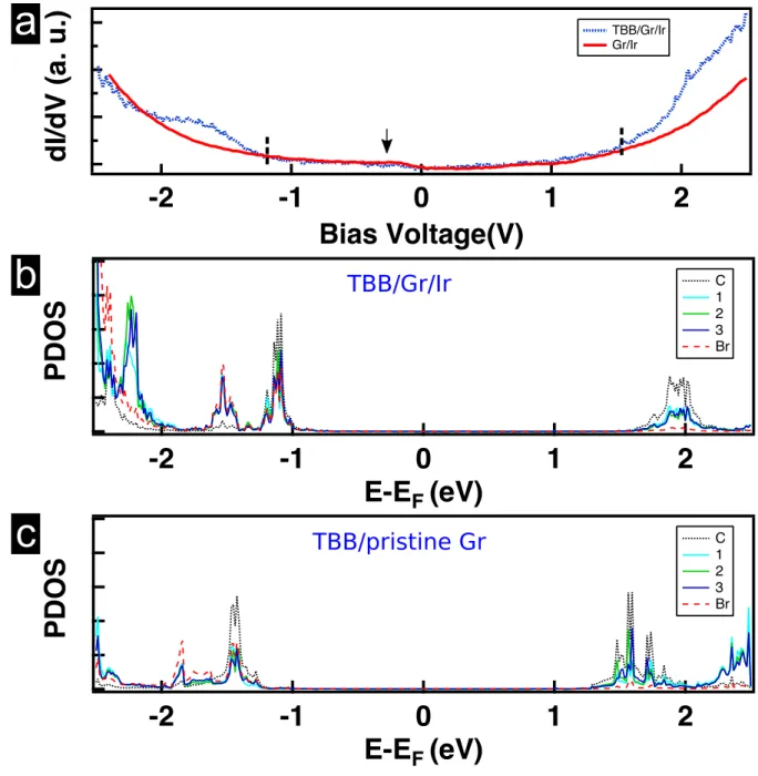
Electronic properties
Finally, we have investigated the electronic properties by LT-STS recorded on bare and
TBB-covered Gr/Ir surface and compared those results with calculated PDOS for free and adsorbed
molecules on different Gr/Ir site (ATOP,FCC) and different orientations with respect to the
substrate (eclipsed or staggered). Experimental dI/dV spectra were averaged over several
unit cells of the two polymorphs. The dI/dV spectrum in Fig. 5(a) of the uncovered Gr/Ir
surface (full red line) reveals one single feature at about -0.280 eV that is attributed to
the Ir surface state that is know to be preserved upon graphene adsorption.49 The dI/dV
spectrum recorded on the 4MOL SAMN is shown as a dotted line in Fig. 5(a). Note that the
one obtained on the 2MOL phase is identical (not shown here). In the range of ±1 eV, the
conductance is dominated by the local density of states of the substrate. Above this range,
extra features that can be attributed to molecular states are observed. The conductance
starts to increase faster than the Gr/Ir one below −1.1 eV and above +1.6 eV leading to a
HOMO-LUMO gap of about 2.7 eV.
The observation than dI /dV spectra are identical for both polymorphs is in good
agree-ment with the fact that the projected density of states (PDOS) of TBB on Gr/Ir varies only
slightly with the adsorption site or the orientation of the molecule as shown in Supporting
Information (Fig. S9 and Fig. S10). In order to measure the impact of the underlying Ir
substrate upon the electronic properties of the system, we have compared the calculated
-600
-400
-200
0
dI/dV (a. u.)
-2
-1
0
1
2
Bias Voltage(V)
TBB/Gr/Ir Gr/Ira
b
10
8
6
4
2
0
PDOS
-2
-1
0
1
2
E-E
F(eV)
C 1 2 3 Br10
8
6
4
2
0
PDOS
-2
-1
0
1
2
E-E
F(eV)
C 1 2 3 Brc
TBB/Gr/Ir
TBB/pristine Gr
Figure 5: (a) Spatially averaged tunneling spectra recorded over Gr/Ir and on a monolayer of 4MOL polymorph on Gr/Ir(111). The arrow points at the Gr/Ir surface state. Pro-jected densities of states (PDOS) of one single TBB molecule adsorbed (b) on a FCC site of Gr/Ir(111) and (c) on pristine Gr. PDOS are projected on different rings 1, 2, 3 and C as labelled in Fig. 1(d) and on bromine atoms.
the addition of Ir layers leads to a rigid shift of the HOMO and LUMO states leaving the
HOMO-LUMO gap unchanged. This can be simply explained by the fact that Ir induces
exper-imentally.46,47 The measured HOMO-LUMO gap of 2.7 eV is much smaller than the one
of a single molecule in gas-phase for which our DFT calculations gives a value of 3.5 eV
(Note that, it is well known that DFT calculations based on semi-local exchange
correla-tion funccorrela-tional severely underestimate HOMO-LUMO gaps.50). This comparison highlights
the fact that the presence of the substrate has a non negligible influence on the electronic
properties of the molecule. The experimental value is in good agreement with our calculated
value of 2.8 eV of TBB on pristine Gr and Gr/Ir (HOMO-LUMO gaps are summarized in
Tab.3). We obtain theoretically for TBB inside a 4MOL SAMN without any substrate, a
HOMO-LUMO gap higher than 3 eV and an electronic state close to the Fermi level (see
in Supporting Information Fig. S11). These two last features are not in agreement with
our STS measurements for which an energy gap between the LUMO and HOMO states of
2.7 eV has been measured and no conductance peak at zero bias (Fermy energy) is observed.
Once again, this leads to the conclusion that the substrate is responsible for a drastic change
in the electronic states. On the contrary, we obtain a very good agreement when
consider-ing the TBB molecule adsorbed on pristine graphene (see in Supportconsider-ing Information, Fig.
S11(b)) or Gr/Ir (Fig. 5(b)) regardless the adsorption site or the orientation of the molecule
with respect to the graphene underlayer (see in Supporting Information Fig. S9 and Fig.
S10). According to the corresponding PDOS, these states are mainly of pz character (see
in Supporting Information Fig. S12). Experimental determination of HOMO and LUMO
energies or HOMO-LUMO gaps of adsorbed TBB are lacking in the literature and do not
allow for a comparative study with other substrate. Nevertheless, a HOMO-LUMO gap of
1.4 eV of TBB adsorbed on boron-doped Si (111) has been calculated.51 It is smaller than
the one obtained in our work for TBB on graphene leading to the conclusion that the Gr/Ir
Table 3: Experimental and computed HOMO-LUMO gaps of the TBB adsorbed on X/(Y) where X is the adsorption site and Y the surface. The symbol ./ is used when the adsorption site is not specified.
Experimental ./(Gr/Ir) 2.7 eV DFT gas-phase 3.5 eV ./(pristine Gr) 2.8 eV FCC/(Gr/Ir) 2.8 eV TOP/(Gr/Ir) 2.8 eV
Conclusions and Perspectives
In summary, low-temperature scanning tunneling microscopy (LT-STM) and density
func-tional theory (DFT) were used to investigate the structural formation of 1,3,5-tri(4’-bromophenyl)benzene
(TBB) self-assembled monolayers on epitaxial graphene on Ir(111). The molecules adsorb
on the Gr/Ir(111) substrate at room temperature and give rise to two distinct and
coex-isting well-ordered phases. Submolecular resolution STM topographs show that the
molec-ular building block of these packings is a pair of TBB molecules. DFT calculations reveal
that in both phases, intermolecular interactions are of C-Br· · · Br and C-Br· · · H type. The
advantages of using Gr/Ir as a support lies in the obtention of highly-ordered molecular
arrangements unperturbated by surface step edges. The high interfacial uniformity is a key
criterion to optimize operation and performances of organic devices. Moreover, the
pres-ence of the graphene moir´e pattern induced by the presence of the Ir layer helped us to
determine the molecular lattices with great accuracy. In addition, we show that the TBB
HOMO-LUMO gap is highly reduced when adsorbed on graphene revealing the non
negli-gible interaction with the substrate. The presence of Ir below graphene induces a charge
transfer from graphene resulting in a rigid shift of the HOMO-LUMO states compared to
pristine graphene. Nevertheless, Ir has only little influence on the adsorption geometry of
the influence of the underlying metal using intercalation for example or the dependence of
the halogen atoms on the molecular arrangements are now required. In addition, molecules
with different symmetries and number of halogen termination could be used to grow novel
molecular architectures. Considering the importance of halogen· · · halogen interactions in
the growth of molecular crystals and the fact that graphene is a promising candidate for
fu-ture electronic devices, this work opens up new routes for the fabrication of next-generation
organic devices.
Experimental section
DFT calculations. In the present study, we have investigated using Density Functional
Theory (DFT) as implemented in the Vienna ab initio simulation package (VASP),52–55
the structural and energetic properties of the two main self assembly TBB structures on
Graphene@Ir(111). The corrugated Graphene@Ir(111) structure was modeled with a (10×10)
Graphene structure over a (9×9) Ir(111) surface cells with 4 atomic layers, as proposed in
different recent studies.56–58 A (10×10) graphene cell was used for the study of the TBB
molecule on the free standing graphene. As usual in this type of calculations, we have
ap-plied a supercell approach, with a vacuum region of more than 20 ˚A to avoid interaction
between periodic images in the z direction. To obtain the reference energy and the
opti-mized structure of a single TBB molecule in gas phase we have used the same cell as the
free standing graphene layer. It has a lattice constant equal to a0 = 2.46 ˚A , close to the
experimentally obtained value (2.459 ˚A ) for a graphite at low temperatures.59
Ions cores were modeled with projector augmented wave (PAW) pseudopotentials.60 The
2s and 2p states of carbon, 1s state of hydrogen and 4s and 4p states of bromine were
treated explicitly in the valence. The plane-wave basis set cutoff energy is set to 400 eV with
a Gaussian smearing method of 0.1 eV width, in order to assure well converged total energy
the optB86b-vdW scheme.61,62 This particular choice of exchange-correlation functional is
based on several previous works.63–67 All the atoms were allowed to relax until the maximum
of all forces acting on them became smaller than 0.02 eV.˚A−1. The k-point sampling was
always based on a Γ-centered grid for all types of calculations. We have used, to optimize
the structures, a single k-point calculation for the TBB molecule, a (4 × 4 × 1) grid for the
TBB-graphene system, a (4 × 4 × 1) grid for 2-TBB, a (3 × 3 × 1) grid for 4-TBB case, when a
(2 × 2 × 1) grid for the single TBB on graphene@Ir(111) system was used. To determine the
density of states (DOS), the tetrahedron integration method with Bl¨ochl corrections68 was
used, with a (6 × 6 × 1) grid for the TBB-graphene and for the TBB on Graphene@Ir(111),
a (7 × 7 × 1) grid for 2MOL and a (5 × 5 × 1) grid for 4MOL.
We have compared the energy stability of two structures, 2MOL and 4MOL, via the
cohesion energy Ecoh of n TBB molecules. This energy can be calculated from the following
equation :
Ecoh = EnMOL− nETBB, (1)
where EnMOL is the total energy of nMOL system and ETBB is the energy of single free TBB
molecule.
Molecule and substrate preparation. The experiments were carried out in an ultra
high vacuum system with a base pressure of 1×10⁻¹⁰mbar equipped with an low-temperature
STM Omicron. The Ir(111) single crystal was cleaned by repeated cycles of Ar+sputtering at
an energy of 1.5 keV followed by a flash annealing to 1100 K. An ordered graphene monolayer
(ML) was prepared by cracking on Ir(111) held at 1100 K under a propene pressure of
3 × 10⁻⁷mbar for 5 min. 1,3,5-tri(4’-bromophenyl)-benzene was purchased from Aldrich and
then purified by column chromatography on silica gel. Then, the molecules were sublimated
using a Knudsen evaporation cell onto a substrate held at room temperature.
STM/STS experiments. All microscopy and spectroscopy measurements were
per-formed at 77 K. The STM images were recorded at a tunneling current IT and a bias voltage
ac-quired with a PtIr tip and a lock-in current detection (bias modulation of 70 mV, frequency
1100 Hz) , in open feedback loop conditions.
Acknowledgment
D. Tristant thanks the Midi-Pyr´en´ees R´egion and the PRES Universit´e de Toulouse for
PhD funding. I. Gerber and D. Tristant also acknowledge the Calcul en Midi-Pyr´en´ees
initiative-CALMIP (Project p0812) for allocations of computer time. Part of this work
was also performed using HPC resources from GENCI-IDRIS and GENCI-CINES (Project
x2015096649). I. Gerber thanks CNRS for financial support.
Supporting Information available
Raw STM images showing both graphene moir´e and molecular lattices. Projected densities
of states of one single TBB molecule adsorbed on various surfaces and geometries. Dihedral
angles of TBB for various adsorption geometries. Computed interatomic distances of the
TBB molecular network. Experimental and computed HOMO-LUMO gaps of the adsorbed
TBB. Optimized geometry of TBB calculated by DFT. Molecular ESP map of TBB in gas
phase.
References
1. Cavallo, G.; Metrangolo, P.; Milani, R.; Pilati, T.; Priimagi, A.; Resnati, G.; Terraneo, G.
The Halogen Bond. Chem. Rev. 2016, 116 , 2478–2601.
2. Griessl, S.; Lackinger, M.; Edelwirth, M.; Hietschold, M.; Heckl, W. M. Self-Assembled
Two-Dimensional Molecular Host-Guest Architectures From Trimesic Acid. Single Mol.
2002, 3 , 25–31.
Phthalo-cyanine Two-Dimensional Network Connected by Hydrogen Bonds. J. Phys. Chem. B
2001, 105 , 10838–10841.
4. Yokoyama, T.; Yokoyama, S.; Kamikado, T.; Okuno, Y.; Mashiko, S. Selective Assembly
on a Surface of Supramolecular Aggregates with Controlled Size and Shape. Nature
2001, 413 , 619–621.
5. Wei, Y.; Tong, W.; Zimmt, M. B. Self-Assembly of Patterned Monolayers with
Nanome-ter Features: Molecular Selection Based on Dipole InNanome-teractions and Chain Length. J.
Am. Chem. Soc. 2008, 130, 3399–3405.
6. Lingenfelder, M. A.; Spillmann, H.; Dmitriev, A.; Stepanow, S.; Lin, N.; Barth, J. V.;
Kern, K. Towards Surface-Supported Supramolecular Architectures: Tailored
Coordina-tion Assembly of 1,4-Benzenedicarboxylate and Fe on Cu(100). Chem. Eur. J 2007, 10 ,
1913–1919.
7. Stepanow, S.; Lin, N.; Payer, D.; Schlickum, U.; Klappenberger, F.; Zoppellaro, G.;
Ruben, M.; Brune, H.; Barth, J. V.; Kern, K. Surface-Assisted Assembly of 2D
Metal-Organic Networks That Exhibit Unusual Threefold Coordination Symmetry. Angew.
Chem. Int. Ed. 2007, 46 , 710–713.
8. Giovannantonio, M. D.; Garah, M. E.; Lipton-Duffin, J.; Meunier, V.; Cardenas, L.;
Revurat, Y. F.; Cossaro, A.; Verdini, A.; Perepichka, D. F.; Rosei, F. et al. Insight into
Organometallic Intermediate and Its Evolution to Covalent Bonding in Surface-Confined
Ullmann Polymerization. ACS Nano 2013, 7 , 8190–8198.
9. Qiu, X.; Wang, C.; Zeng, Q.; Xu, B.; Yin, S.; Wang, H.; Xu, S.; Bai, C. Alkane-Assisted
Adsorption and Assembly of Phthalocyanines and Porphyrins. J. Am. Chem. Soc. 2000,
122 , 5550–5556.
Perepichka, D. F.; Rosei, F. Crystal Engineering in Two Dimensions: An Approach to
Molecular Nanopatterning. J. Phys. Chem. C 2007, 111 , 16996–17007.
11. ger, D. B.; Kreher, D.; Mathevet, F.; Attias, A.-J.; Schull, G.; Huard, A.; Douillard, L.;
Fiorini-Debuischert, C.; Charra, F. Surface Noncovalent Bonding for Rational Design of
Hierarchical Molecular Self-Assemblies. Angew. Chem. Int. Ed. 2007, 46 , 7404–7407.
12. Grimme, S. Do Special Noncovalent pi-pi Stacking Interactions Really Exist? Angew.
Chem. Int. Ed. 2008, 47 , 3430–3434.
13. MacLeod, J. M.; Rosei, F. Molecular Self-assembly on Graphene. Small 2014, 10 , 1038–
1049.
14. Marchini, S.; G¨unther, S.; Wintterlin, J. Scanning Tunneling Microscopy of Graphene
on Ru(0001). Phys. Rev. B 2007, 76 , 075429.
15. N’Diaye, A. T.; Coraux, J.; Plasa, T. N.; Busse, C.; Michely, T. Structure of Epitaxial
Graphene on Ir(111). New J. Phys. 2008, 10 , 043033.
16. Sicot, M.; Bouvron, S.; Zander, O.; Rudiger, U.; Dedkov, Y. S.; Fonin, M. Nucleation
and Growth of Nickel Nanoclusters on Graphene Moir´e on Rh(111). Appl. Phys. Lett.
2010, 96 , 093115.
17. Land, T. A.; Michely, T.; Behm, R. J.; Hemminger, J. C. STM Investigation of Single
Layer Graphite Structures Produced on Pt (111) by Hydrocarbon Decomposition. Surf.
Sci. 1992, 264, 261–270.
18. Cai, Y.; Zhang, H.; Song, J.; Zhang, Y.; Bao, S.; He, P. Adsorption Properties of CoPc
Molecule on Epitaxial Graphene/Ru(0001). Appl. Surf. Sci. 2015, 327 , 517–522.
19. Mao, J.; Zhang, H.; Jiang, Y.; Pan, Y.; Gao, M.; Xiao, W.; Gao, H. J. Tunability of
Supramolecular Kagome Lattices of Magnetic Phthalocyanines Using Graphene-Based
20. Scheffler, M.; Smykalla, L.; Baumann, D.; Schlegel, R.; H¨anke, T.; M.Toader,;
B¨uchner, B.; Hietschold, M.; Hess, C. Structural Study of Monolayer Cobalt
Phthalo-cyanine Adsorbed on Graphite. Surf. Sci. 2013, 608 , 55–60.
21. ˚Ahlund, J.; Schnadt, J.; Nilson, K.; G¨othelid, E.; Schiessling, J.; Besenbacher, F.;
M˚artensson, N.; Puglia, C. The Adsorption of Iron Phthalocyanine on Graphite: A
Scanning Tunnelling Microscopy Study. Surf. Sci. 2007, 601 , 3661–3667.
22. Yang, K.; Xiao, W. D.; Jiang, Y. H.; Zhang, H. G.; Liu, L. W.; Mao, J. H.; Zhou, H. T.;
Du, S. X.; Gao, H. J. Molecule-Substrate Coupling between Metal Phthalocyanines and
Epitaxial Graphene Grown on Ru(0001) and Pt(111). J. Phys. Chem. C 2012, 116 ,
14052–14056.
23. Shikin, A. M.; Prudnikova, G. V.; Adamchuk, V. K.; Moresco, F.; Rieder, K.-H. Surface
Intercalation of Gold Underneath a Graphite Monolayer on Ni(111) Studied by
Angle-Resolved Photoemission and High-Resolution Electron-Energy-Loss Spectroscopy. Phys.
Rev. B 2000, 62 , 13202.
24. Dedkov, Y. S.; Shikin, A. M.; Adamchuk, V. K.; Molodtsov, S. L.; Laubschat, C.;
Bauer, A.; Kaindl, G. Intercalation of Copper Underneath a Monolayer of Graphite on
Ni(111). Phys. Rev.B 2001, 64 , 035405.
25. Varykhalov, A.; S´anchez-Barriga, J.; Shikin, A. M.; Biswas, C.; Vescovo, E.;
Ry-bkin, A.; Marchenko, D.; Rader, O. Surface Intercalation of Gold Underneath a Graphite
Monolayer on Ni(111) Studied by Angle-Resolved Photoemission and High-Resolution
Electron-Energy-Loss Spectroscopy. Phys. Rev. B 2000, 62 , 13202.
26. Enderlein, C.; Kim, Y. S.; Bostwick, A.; Rotenberg, E.; Horn, K. The Formation of an
Energy Gap in Graphene on Ruthenium by Controlling the Interface. New J. Phys 2010,
27. Sutter, P.; Sadowski, J. T.; Sutter, E. A. Chemistry under Cover: Tuning
Metal-Graphene Interaction by Reactive Intercalation. J. Am. Chem. Soc. 2010, 132 , 8175–
8179.
28. Rutkov, E. V.; Gall, N. R. Intercalation of Graphene Films on Metals with Atoms and
Molecules, Physics and Applications of Graphene - Experiments. Dr. Sergey Mikhailov
(Ed.), InTech
29. Sicot, M.; Leicht, P.; Zusan, A.; Ole Zander, M. W.; Dedkov, Y. S.; Horn, K.
Size-Selected Epitaxial Nanoislands Underneath Graphene Moir´e on Rh(111). ACS Nano
2012, 6 , 151–158.
30. Sicot, M.; Fagot-Revurat, Y.; Vasseur, G.; Kierren, B.; Malterre, D. Copper Intercalation
at the Interface of Graphene and Ir(111) Studied by Scanning Tunneling Microscopy.
Appl. Phys. Lett. 2014, 105 , 191603.
31. Bazarnik, M.; Brede, J.; Decker, R.; Wiesendanger, R. Tailoring Molecular Self-Assembly
of Magnetic Phthalocyanine Molecules on Fe- and Co-intercalated Graphene. ACS Nano
2013, 7 , 11341–11349.
32. Schumacher, S.; Wehling, T. O.; Lazi´c, P.; Runte, S.; rster, D. F. F.; Busse, C.;
Petrovi´c, M.; Kralj, M.; Bl¨ugel, S.; Atodiresei, N. et al. The Backside of Graphene:
Manipulating Adsorption by Intercalation. Nano Lett. 2013, 13 , 5013–5019.
33. Coraux, J.; N’Diaye, A. T.; Busse, C.; Michely, T. Structural Coherency of Graphene on
Ir(111). Nano Lett. 2008, 8 , 565–570.
34. Sutter, P. W.; Flege, J.-I.; Sutter, E. A. Epitaxial Graphene on Ruthenium. Nat. Mater.
2008, 7 , 406–411.
Self-Assembly of Cobalt-Phthalocyanine Molecules on Epitaxial Graphene on Ir(111). J.
Phys. Chem. C 2012, 116, 20433–20437.
36. Gatti, R.; MacLeod, J. M.; Lipton-Duffin, J. A.; Moiseev, A. G.; Perepichka, D. F.;
Rosei, F. Substrate, Molecular Structure, and Solvent Effects in 2D Self-Assembly via
Hydrogen and Halogen Bonding. J. Phys. Chem. C 2014, 118 , 25505–25516.
37. Gutzler, R.; Walch, H.; Eder, G.; Kloft, S.; Heckl, W.; Lackinger, M. Surface
medi-ated synthesis of 2D covalent organic frameworks: 1,3,5-tris(4-bromophenyl)benzene on
graphite(001),Cu(111)and Ag(110). Chem. Comm. 2009, 29 , 4456–4458.
38. Silly, F. Selecting Two-Dimensional Halogen–Halogen Bonded Self-Assembled
1,3,5-Tris(4-iodophenyl)benzene Porous Nanoarchitectures at the Solid–Liquid Interface. J.
Phys. Chem. C 2013, 117 , 20244–20249.
39. Baris, B.; Luzet, V.; Duverger, E.; Sonnet, P.; Palmino, F.; Cherioux, F. Robust and
Open Tailored Supramolecular Networks Controlled by the Template Effect of a Silicon
Surface. Angew. Chem. Int. Ed. 2011, 50, 4094–4098.
40. Walch, H.; Gutzler, R.; Sirtl, T.; Eder, G.; Lackinger, M. Material- and
Orientation-Dependent Reactivity for Heterogeneously Catalyzed Carbon-Bromine Bond Homolysis.
J. Phys. Chem. C 2010, 114 , 12604–12609.
41. Blunt, M. O.; Russell, J. C.; Champness, N. R.; Beton, P. H. Templating Molecular
Adsorption Using a Covalent Organic Framework. Chem. Commun. 2010, 46 , 7157–
7159.
42. Russell, J. C.; Blunt, M. O.; Garfitt, J. M.; Scurr, D. J.; Alexander, M.;
Champ-ness, N. R.; Beton, P. H. Dimerization of Tri(4-bromophenyl)benzene by Aryl-Aryl
43. Capdevila-Cortada, M.; Novoa, J. J. The Nature of the C–Br...Br–C
Intermolecu-lar Interactions Found in MolecuIntermolecu-lar Crystals: a General Theoretical-Database Study.
CrystEngComm 2015, 17 , 3354–3365.
44. Murray, J.; Lane, P.; Politzer, P. Expansion of the sigma-Hole Concept. J. Mol. Model.
2009, 15 , 723–729.
45. Politzer, P.; Murray, J. S.; Clark, T. Halogen Bonding and Other sigma-Hole Interactions:
A Perspective. Phys. Chem. Chem. Phys. 2013, 15 , 11178–11189.
46. Preobrajenski, A.; Ng, M. L.; Vinogradov, A. S.; rtensson, N. M. Controlling Graphene
Corrugation on Lattice-Mismatched Substrates. Phys. Rev. B 2008, 78 , 073401.
47. Pletikosi´c, I.; Kralj, M.; Pervan, P.; Brako, R.; Coraux, J.; N’Diaye, A. T.; Busse, C.;
Michely, T. Dirac Cones and Minigaps for Graphene on Ir(111). Phys. Rev. Lett. 2009,
102 , 056808.
48. Beltran, L. M. C.; Cui, C.; Leung, D. H.; Xu, J.; Hollander, F. J.
1,3,5-Tris(p-bromophenyl)benzene. Acta Crystallogr., Sect. E: Struct. Rep. Online 2002, 58 , o782–
o783.
49. Pletikosi´c, I.; Kralj, M.; ˇSokˇcevi´c, D.; Brako, R.; Lazi´c, P.; Pervan, P. Photoemission and
Density Functional Theory Study of Ir(111); Energy Band Gap mapping. J. of Phys.:
Condens. Matter 2010, 22 , 135006.
50. Zhang, G.; Musgrave, C. B. Comparison of DFT Methods for Molecular Orbital
Eigen-value Calculations. J. Phys. Chem.A 2007, 111 , 1554–1561.
51. Boukari, K.; Duverger, E.; Sonnet, P. Full DFT-D Description of a Nanoporous
Supramolecular Network on a Silicon Surface. J. Chem. Phys. 2013, 138 , 084704–084713.
52. Kresse, G.; Hafner, J. Ab Initio Molecular Dynamics for Liquid Metals. Phys. Rev. B
53. Kresse, G.; Hafner, J. Ab Initio Molecular-Dynamics Simulation of the
Liquid-Metal-Amorphous-Semiconductor Transition in Germanium. Phys. Rev. B 1994, 49 , 14251.
54. Kresse, G.; Furthm¨uller, J. Efficient Iterative Schemes for Ab Initio Total-Energy
Cal-culations Using a Plane-Wave Basis Set. Phys. Rev. B 1996, 54 , 11169.
55. Kresse, G.; Furthm¨uller, J. Efficiency of Ab-Initio Total Energy Calculations for Metals
and Semiconductors Using a Plane-Wave Basis Set. Com. Mat. Sci. 1996, 6 , 15–50.
56. Brako, R.; ˇSokˇcevi´c, D.; Lazi´c, P.; Atodiresei, N. Graphene on the Ir(111) Surface: from
Van Der Waals to Strong Bonding. New J. Phys 2010, 12 , 113016.
57. Busse, C.; Lazi´c, P.; Djemour, R.; Coraux, J.; Gerber, T.; Atodiresei, N.; Caciuc, V.;
Brako, R.; N’Diaye, A. T.; Bl¨ugel, S. et al. Graphene on Ir(111): Physisorption with
Chemical Modulation. Phys. Rev. Lett. 2011, 107 , 036101.
58. Vita, H.; B¨ottcher, S.; Horn, K.; Voloshina, E. N.; Ovcharenko, R. E.; Kampen, T.;
Thissen, A.; Dedkov, Y. S. Understanding the Origin of Band Gap Formation in
Graphene on Metals: Graphene on Cu/Ir(111). Sci. Rep. 2014, 4 , 5704–5712.
59. Baskin, Y.; Meyer, L. Lattice Constants of Graphite at Low Temperatures. Phys. Rev.
1955, 100, 544.
60. Bl¨ochl, P. E. Projector Augmented-Wave Method. Phys. Rev. B 1994, 50 , 17953.
61. Klimeˇs, J.; Bowler, D. R.; Michaelides, A. Chemical Accuracy for the Van Der Waals
Density Functional. J. Physics: Condens. Matter 2010, 22 , 022201.
62. Klimeˇs, J.; Bowler, D. R.; Michaelides, A. Van der Waals Density Functionals Applied
to Solids . Phys. Rev. B 2011, 83 , 195131.
63. Tristant, D.; Puech, P.; Gerber, I. C. Theoretical Study of Graphene Doping Mechanism
64. Hu, T.; Gerber, I. C. Theoretical Study of the Interaction of Electron Donor and Acceptor
Molecules with Graphene. J. Phys. Chem. C 2013, 117 , 2411–2420.
65. Hu, T.; Gerber, I. C. Band gap Modulation of Bilayer Graphene by Single and Dual
Molecular Doping: A van der Waals Density-Functional Study. Chem. Phys. Lett. 2014,
616 , 75–80.
66. Kong, L.; Enders, A.; Rahman, T. S.; Dowben, P. A. Molecular Adsorption on Graphene.
J. Phys.: Condens. Matter 2014, 26 , 443001.
67. Tristant, D.; Wang, Y.; Gerber, I.; Monthioux, M.; P´enicaud, A.; Puech, P. Optical
Signatures of Bulk and Solutions of KC8 and KC24. J. Appl. Phys. 2015, 118 , 044304.
68. Bl¨ochl, P. E.; Jepsen, O.; Andersen, O. K. Improved Tetrahedron Method for
Brillouin-Zone Integrations. Phys. Rev. B 1994, 49 , 16223.