HAL Id: hal-02060353
https://hal.archives-ouvertes.fr/hal-02060353
Submitted on 7 Mar 2019
HAL is a multi-disciplinary open access
archive for the deposit and dissemination of
sci-entific research documents, whether they are
pub-lished or not. The documents may come from
teaching and research institutions in France or
abroad, or from public or private research centers.
L’archive ouverte pluridisciplinaire HAL, est
destinée au dépôt et à la diffusion de documents
scientifiques de niveau recherche, publiés ou non,
émanant des établissements d’enseignement et de
recherche français ou étrangers, des laboratoires
publics ou privés.
nanostructures. I. Electron-hole collective processes in
single Si ∕ Si O 2 quantum wells
N. Pauc, V. Calvo, J. Eymery, F. Fournel, N. Magnea
To cite this version:
N. Pauc, V. Calvo, J. Eymery, F. Fournel, N. Magnea. Electronic and optical properties of Si ∕ Si O
2 nanostructures. I. Electron-hole collective processes in single Si ∕ Si O 2 quantum wells. Physical
Review B: Condensed Matter and Materials Physics (1998-2015), American Physical Society, 2005, 72
(20), �10.1103/PhysRevB.72.205324�. �hal-02060353�
Electronic and optical properties of Si/ SiO
2nanostructures. I. Electron-hole collective processes
in single Si/ SiO
2quantum wells
N. Pauc,1,*V. Calvo,1,†J. Eymery,1F. Fournel,2and N. Magnea1
1CEA Grenoble, DRFMC/SP2M/SiNaPS, 17 rue des Martyrs, 38054 Grenoble Cedex 9, France 2CEA-DRT-LETI, CEA/GRE, 17 rue des Martyrs, 38054 Grenoble Cedex 9, France
共Received 3 June 2005; published 18 November 2005兲
Photoluminescence measurements have been performed at low temperature on crystalline Si/ SiO2quantum wells as a function of thickness. Three distinct electron-hole 共e-h兲 phases are clearly identified in these structures: the electron-hole liquid, the electron-hole plasma, and the free-exciton gas. It is shown that spatial confinement induced by the SiO2 barriers modifies the thermodynamical equilibrium between these phases
with respect to the bulk case by changing the steady state of the carrier system and involving new transient states. In the low-thickness domain, the e-h recombination line blueshifts as a result of the effect of quantum confinement on the band-edge positions. Data are analyzed thanks to a model taking account of the new band-diagram parameters—effective mass, band degeneracy, anisotropy—and image charges in the dielectric barrier which modify the strength of Coulomb interactions between carriers in the Si well. Results interpreted in the frame of a simple coalescence model indicate that the two-dimensional electron-hole liquid forms a cloud of in-plane pancakes. Finally, an attempt is made here to compute the phase diagram of carriers in varying-thickness quantum wells by means of a spin-1 lattice-gas model and to predict the nature of the two-dimensional e-h collective state.
DOI:10.1103/PhysRevB.72.205324 PACS number共s兲: 73.21.Fg, 78.55.⫺m, 78.67.De, 05.30.Fk
I. INTRODUCTION
In 1966 Haynes1observed a broad line in the photolumi-nescence共PL兲 spectra of bulk Si submitted to strong optical pumping. This new line, arising on the low-energy side of the free-exciton共FE兲 peak, was first attributed by the author to the radiative recombination of carriers in the excitonic molecule—namely, an entity composed of two electrons and two holes. In 1968, Keldysh2 analyzed the results of Asnin and Rogachev3who observed a sudden jump in the conduc-tivity of bulk Ge samples under variable-power illumination as the metallization of excitons. These results lead to a rein-terpretation of Haynes’ data and to attribute the broad low-energy line to a new electron-hole共e-h兲 phase, the electron-hole liquid共EHL兲. This condensed phase is obtained when excitons overlap and cannot form a bound state—that is, for sufficiently high excitonic densities. The band structure of Si is particularly suitable for the formation of EHL in view of the long exciton lifetime共of the order of 1s兲 resulting from the indirect nature of the band gap and from the orbital de-generacy of valence and conduction bands which lowers the positive kinetic part of the free energy per e-h pair.
Condensation of excitons in EHL was widely studied in bulk semiconductors during the 1960s and 1970s. It was therefore possible to compare the results of the many-body calculations to experimental measurements by considering several parameters such as EHL equilibrium density, kinetic, exchange, and correlation energies, etc. An excellent over-view of the work accomplished in the field of EHL can be found in the review article by Rice et al.4
The overwhelming rise of the microelectronics industry during the past two decades has involved a significant im-provement in nanofabrication techniques, particularly in the realization of silicon-based nanostructures with a very good
crystallinity and a moderate concentration of nonradiative recombination centers at the Si/ SiO2 interface. It is nowa-days possible to make artificial Si/ SiO2 heterostructures— namely, silicon-on-insulator共SOI兲 wafers, where a SiO2/ Si stack lies on a bulk-crystalline Si substrate after a molecular bonding stage.5,6 The standard values for the SiO
2 and Si layers are set to 400 and 200 nm, respectively. A final ther-mal oxidation stage of the superficial crystalline Si 共c-Si兲 layer is necessary to create a second barrier for the motion of carriers in the Si quantum well 共QW兲 and to passivate the superficial defects. The resulting structure can be considered as a c-Si QW with quasi-infinite-height dielectric barriers of 3.2 eV for the electrons and 5 eV for the holes.
In 1998, Tajima and Ibuka7showed by continuous wave 共cw兲 PL experiments that EHL could form in such structures. This discovery opened new opportunities for the study of EHL in low-dimensional Si samples.8,9 Indeed, the QW thickness lz can easily be tuned from the 200-nm standard
value down to a thinner one by several thermal oxidation and HF etching deoxidation cycles. The excellent insulating, structural, and growth properties of the Si oxide give us a unique opportunity for the study of the various e-h phases and the Coulomb interactions between carriers in these Si QW’s. In particular, interesting phenomena related to quan-tum confinement and mismatch of the dielectric constants in the heterostructure are expected to occur in narrow quantum wells with thickness of the order of the bulk excitonic Bohr radius ax共ax⬇4.9 nm in crystalline silicon兲.
In this article, we present PL studies of c-Si QW’s with thickness varying between 190 and 4.7 nm. Several regimes are identified according to the thickness domain. For 190 nm艌lz艌3ax⬇15 nm and within the spatial
confine-ment regime, a first change in the thermodynamics of the e-h phases with respect to bulk Si is evidenced in c-Si QW’s. For
ax⬇4 nm艋lz艋3ax⬇15 nm, in the weak quantum
confine-ment regime, the EHL line shifts moderately towards high energies as a result of the quantum confinement effect on the band-edge positions. An attempt is made to account for these experimental results. The effect of image charges is included in a model that takes account of the low QW thickness thanks to a varying-lzscreened Coulomb potential. The
ques-tion of the nature of the condensed phase in such QW’s will be examined: Do we create an incompressible liquid or a compressible gas? A simple coalescence model will be used here to describe the spatial distribution of the two-dimensional EHL.
II. SAMPLES AND EXPERIMENT
The c-Si QW’s are obtained from 8 in. SOI wafers where the c-Si and thermal SiO2layers have been transferred on a bulk Si substrate via molecular bonding. The variable-thickness c-Si QW set with lz ranging from 15 to 190 nm
originates from a series of thermally oxidized SOI wafers. The well thickness is defined by the amount of consumed c-Si during one or several oxidation-sacrificial deoxidation cycles resulting in a 400-nm buried oxide/ lz-nm
c-Si/ 10– 40 nm superficial oxide stack. We made a set of Si/ SiO2 QW’s in the 5 nm艋lz艋15 nm thickness range.
Several mm2-sized homogeneous samples can be obtained due to slow thickness variations with the lateral position. For each sample, we checked the thicknesses of the stack by means of spectroscopic ellipsometry. The accuracy of these measurements, confirmed by x-ray reflectivity, has been found to be lower than ±0.5 nm.
Samples were placed in a variable-temperature helium cir-culation cryostat with temperature T varying between 4 and 300 K. For cw PL experiments, we used a standard lock-in technique—i.e., a mechanically chopped Ar+ cw laser, a 640-mm monochromator, and a photomultiplier tube with cooled InGaAs photocathode. The laser power reaches 100 mW under cw operation with a spot diameter Dnf
⬇1250m and Df⬇55m in the nonfocused and focused
modes, respectively. The corresponding laser density powers P are found to be in the W cm−2 and kW cm−2 ranges. We recorded a white lamp spectrum共blackbody at 3400 K兲 and used it as a correction function of the spectra. We worked with the 351-nm共3.53-eV兲 laser line which provides strong absorption in the direct gap of c-Si and thus efficient pump-ing of silicon nanostructures. The absorbed part A of incident power by the c-Si QW’s is assumed to obey the law A共lz兲
=共1−R兲共1−exp关−␣lz兴兲 for a given lz, where ␣= 9
⫻1015cm−1 at=351 nm is the inverse of the penetration length of laser beam in c-Si 共Ref. 10兲 and R the reflected part. For time-resolved spectroscopy, we used a tripled Nd:YAG pulsed laser with 350 nm emission共duration pulse of 10 ns and variable repetition rate兲 and photon counting method to recover the signal.
III. SPATIAL CONFINEMENT REGIME A. Effects at the thermodynamical steady-state equilibrium
The first step towards a best understanding of exciton condensation in confined media lies in identifying the
dis-tinct e-h phases generated in thick c-Si QW’s and comparing them to the well-known EHL, EHP, and FE phases in bulk material. As shown in Fig. 1, one can see PL spectra obtained from a 100-nm QW for T = 6, 15, and 35 K and variousP. For T = 6 K andP=4⫻103 W cm−2the broad and asymmet-ric quasidegenerate TO-LO phonon replica of EHL in bulk Si arise in the PL spectrum at 1.081 eV. No energetic shift of the recombination lines is observed between 6.5 and 4 ⫻103W cm−2as a result of the constant density of the liquid in the QW under variable density of injected carriers. The slight redshift of the EHL line when P passes from 0.5 to 6.5 W cm−2 is attributed to the coalescence of EHL droplets. This phenomenon has been described in a previous paper8and is not the topic of this article.
A more accurate description of EHL ground-state param-eters such as e-h pair density n or temperature can be given thanks to the line-shape analysis. EHL can be viewed as two degenerate incompressible gas of electrons and holes, each one with its own Fermi quasilevel EF
e
and EF h
. Coulomb in-teractions between carriers lead to a band-gap renormalization—i.e., a decrease in the band-gap energy Eg
by an amount ⌬EBGR, due to many-body phenomena.
Fol-lowing Rice,11 we assume a rigid band shift without mass renormalization for electrons 共me= 1.08兲 and holes 共mh
= 0.55兲. The PL line shape is given by the product of convo-lution of the e-h populations and is written
I共h兲 = I0
冕
0 h¯ De共⑀兲Dh共h¯ − ⑀兲 ⫻ f共⑀,EF e兲f共h¯ − ⑀ ,EF h兲d⑀ , 共1兲 where the prefactor I0 is constant, h is the photon energy, De,h共⑀兲 are the tridimensional e-h density of statespropor-FIG. 1. Photoluminescence spectra obtained from a 100-nm c-Si QW at T = 6, 15, and 35 K and P=0.5,6.5,50,150, and 4 ⫻103W cm−2.
tional to
冑
⑀, f is the Fermi distribution, h¯ = h − Eg−⌬EBGR+បTO with បTO= 58.3 meV, the band-gap
renor-malization energy⌬EBGR given in Ref. 12, and EF e
and EF h
given in Ref. 13.
The model line shape I is a function of three parameters I0, n, and T, since EFe,h and⌬EBGR depend on 共n,T兲 and n,
respectively. A very convenient and accurate analytical form of the model function has been used here, where the continu-ous sum in Eq. 共1兲 has been replaced by a discrete sum following the Gauss-Legendre integration method of order j = 12.14Minimizing the2function with respect to共I
0, n , T兲 gives the experimental density nexptand temperature Texptfor
the EHL or EHP phases. Results from fits performed on the 100-nm QW spectrum for T = 6 K and P=4 kW cm−2 yield nexpt= 3.19⫻1018cm−3, in very good agreement with
theo-retical calculations and experimental values of the equilib-rium density of EHL in bulk silicon.4 In Fig. 1, the fitted curve共circular symbol兲 is very close to the experimental data curve. We can conclude that at low temperatures EHL is stable in thick c-Si QW’s and has the same ground-state parameters than in bulk samples. The fit temperature Texpt
= 19 K is found to be higher than the monitored temperature 共6 K兲 for the highest pumping power—i.e., 4 kW cm−2—whereas T
expt= 12 K for moderate pumping
powers—i.e., 6.5 W cm−2. This discrepancy arises from local heating of the sample by a laser spot which is reinforced by inefficient heat transfer outside the well due to the thermal insulating properties of the silica barriers. Fortunately, Texpt
is lower than the liquid-plasma transition temperature Tc
= 28 K in bulk c-Si. Therefore, the laser heating does not prevent e-h pair condensation in EHL in c-Si QW’s.
In the spectra of Fig. 1 recorded at 15 K and for the low P, one can see the two characteristic TO-LO phonon replica of FE resulting in a narrow line centered at 1.098 eV, as in bulk c-Si.4Due to many-body phenomena, EHL droplets can be viewed as potential traps for carriers with a barrier height or work function equal to⌽⬇8 meV.4Thus evaporation of e-h pairs from EHL droplets to form excitons in QW’s is thermally activated, as shown in Fig. 1 when T increases from 6 to 15 K forP=6.5 W cm−2. As P and the mean car-rier density具n典 increase, the EHL line intensity increases at the expense of the FE one. This change in the relative am-plitudes of the recombination lines can be explained by the phase diagram of carriers in silicon:4an increase in具n典 modi-fies the thermodynamical equilibrium between FE and EHL phases towards an increase in the ratio of “liquid” e-h pairs. The ability to modulate具n典 by varying P in the SOI samples is due to the so-called “spatial confinement” effect caused by the dielectric barriers which prevents carriers diffusion in the c-Si substrate. In bulk c-Si, the high diffusion length of car-riers, of the order of 100m,4induces a density gradient in the sample and a lowering of具n典 with respect to c-Si QW’s. In this case and in the frame of the theory of phase diagrams, no direct relation betweenP and 具n典 can be given to account for the relative amplitudes of the FE and EHL lines.
The spectra recorded for T = 35 K show a clear blueshift of the e-h recombination line as P decreases. This shift is ascribed to a lowering of the absolute value of the renormal-ization energy ⌬EBGR resulting from a decrease in the e-h
fluid density n.12This allows us to identify this fluid with the electron-hole plasma共EHP兲 which has been found to be the stable condensed e-h phase above T⬇28 K in bulk silicon.15,16 As a consequence, we deduce that the liquid-plasma transition temperature Tcin the 190-nm c-Si QW is
likely close to its bulk value—strictly speaking and accord-ing to the spectra acquired at T = 15 and 35 K as shown in Fig. 1 for P=6.5 W cm−2, Tc is found be in the 15– 35 K
range, in qualitative agreement with the theoretical and ex-perimental bulk values. In the case of very low pumping powers we can see two contributions in the PL spectra which correspond to the convergence of the EHP line towards the FE one. Finally, for the lowestP, the only stable e-h system in the QW is the FE phase. The observed progressive change in the ratio of EHP and FE lines is an example of the Mott transition between the metallic EHP and the insulating FE phases which occurs not only in bulk c-Si17but also here in the c-Si QW’s.
The spatial confinement effect is a very useful phenom-enon which helps us in determining the different phase den-sities in the QW. Considering the high diffusion length of carriers with respect to the well thickness, one can assume a total filling of the QW in EHP or FE phases, for the very-high- and very-low-P regimes where no mixing between EHP and FE occurs. Measuring the lifetimep,eof e-h pairs
in EHP and FE phases for the 190-nm QW at 35 K allows us to calculate the plasma or excitonic pair densities np,eas
np,e⬇ P
p,e共1 − R兲
lzh
, 共2兲
where R⬇0.55 is the reflection coefficient of laser beam on the SOI surface.
Assuming that the Mott transition for carriers in the 190-nm QW occurs between P=6.5 and 0.5 W cm−2 and taking p= 800 ns and e= 2700 ns for the 190-nm QW at 35 K, Eq. 共2兲 yields np= 2.7⫻1017cm−3 and ne= 6.8
⫻1016cm−3—note that the excitonic contribution in the 6.5 W cm−2 spectrum in Fig. 1 has been neglected. Knowl-edge of the Debye-Huckel screening length DH
=共2e2n /⑀0⑀SikBT兲−1/2, where ⑀Si= 11.4 is the dielectric
con-stant of c-Si, allows us to calculate the Mott density nMwith
the condition18
DH共n艌nM兲艋0.84axwhich gives
nM共T兲 =
1.192⑀0⑀SikBT
2e2ax
2 . 共3兲
Thanks to Eq. 共3兲, for T=35 K, we find nM⬇5.3
⫻1016cm−3. This theoretical value is somewhat smaller than the measured experimental one in the 6.8⫻1016– 2.7 ⫻1017cm−3range. This discrepancy can be corrected by tak-ing into account the lateral diffusion of carriers along the QW which induces a lowering of n as calculated with Eq. 共2兲. When carriers are generated by a Dnf= 1250m
diam-eter laser spot with P=0.5 W cm−2, the exciton diffusion length LEX=
冑
DEXEX⬇630m, with DEX= 1500 cm2s−14,gives the characteristic radial spreading of the e-h system. The density given in Eq.共2兲 should be modified and divided by a density correction factor c to take account of the lateral diffusion of carriers. Here, the evaluation of c is
straightfor-ward and gives c =关共Dnf/ 2 + LEX兲/Dnf/ 2兴2⬇4 and results in a
more accurate estimate of the experimental density nMin the
1.7⫻1016– 6.75⫻1016cm−3 range, in good agreement with the theoretical values.
The former approach used to calculate n is simple and crude but the good estimate of nMsupports our hypothesis on
the limited expansion of an EHP or a FE gas between the SiO2 barriers—i.e., the spatial confinement effect.
Another striking effect relative to the spatial confinement phenomenon can be observed in Fig. 2 by comparing the PL spectra of a 190-nm c-Si QW and a bulk c-Si under the same conditions of illumination and temperature. For either T = 6 or 15 K andP=6.5 W cm−2, we can see that the PL spectra of the bulk sample only exhibit the FE line, whereas those of the QW contain the two EHL and FE contributions. We con-clude that the exciton condensation threshold as a function of P is lowered in the Si-confined systems such as SOI QW’s, due to the limited two dimensional diffusion of carriers.
We would like to point out that the photoconduction ex-periment of Asnin and Rogachev3performed in bulk germa-nium could be particularly interesting when applied in our samples. Indeed, spatial confinement along with the ability to control the geometry of the Ohmic contacts at the QW sur-face allow not only accurate measurement of the carrier den-sity but also measurement of the fluid resistivity between the two electrodes. Measuring the position of the conductivity jump by increasing the laser power would give an accurate estimate of the Mott density. In addition, in case of total filling of the QW volume by the EHL at high P, measure-ment of the EHL resistivity is expected to give precious in-formation on its metallic nature and on the “hydrodynami-cal” properties of this condensed phase.
B. Dynamical effects
Under cw operation, the EHL, EHP, and FE phases are in a thermodynamical steady-state equilibrium since the ther-malization time of carriers 共of the order of 1⫻10−12s兲 is several orders of magnitude smaller than the e-h lifetime共of
the order of 1⫻10−6s兲. Due to the long integration time of the PL signal by our lock-in amplifier in the cw PL detection display共of the order of 1⫻10−3s兲, no dynamical effects can be observed. To overcome this problem, we performed time-resolved PL measurements with a pulsed laser and a digital counter. Two adjustable time parameters are used: the time delay共D兲 after the end of the laser pulse to open the count-ing window and the width共W兲 of the counting window.
Time-resolved PL spectra have been recorded on bulk c-Si and the 190-nm c-Si QW samples, as shown in Figs. 3共a兲 and 3共b兲 for various temperatures, delays, and widths. D and W are set to small values to avoid the “time integration phenomenon” which would cause distortion of PL spectra towards a “classical” equilibrium line shape.
We can see in Fig. 3共a兲 that the spectrum recorded under pulsed operation for D = 0 ns, W = 10 ns, and T = 10 K on the bulk c-Si is close to the TO-LO EHL replica observed under cw operation. The slight energetic shift between these two spectra might be due to e-h recombination in small EHL
FIG. 2. Comparison between PL spectra from a 190 nm c-Si QW and pure bulk c-Si floating zone共FZ兲 under the same power densityP=6.5 W cm−2for T = 6 and 15 K.
FIG. 3. 共a兲 Solid and circle lines: time-resolved PL spectra ob-tained on bulk c-Si for a delay after pulse D = 0 ns and a width of the counting window W = 10 ns as a function of temperature and
D = 25 ns and W = 10 ns at T = 10 K respectively.共b兲 Solid lines and
circles: time-resolved PL spectra obtained on a 190-nm c-Si QW as a function of D and W and fits, respectively. Dotted line: PL spec-trum of c-Si under cw operation at T = 10 K for共a兲 and 共b兲.
droplets in maturation at short delays. Such a blueshift has also been observed under cw operation in thin QW’s at low temperatures and ascribed to carrier recombination via the fundamental states of a “nanodroplet,” viewed as a three-dimensional 共3D兲 harmonic oscillator for electrons and holes.8 With increasing D—i.e., for D = 25 ns and W = 10 ns—the EHL line redshifts and has the same low-energy cutoff as the cw EHL line corresponding to macro-scopic droplets. Thus, the maturation time necessary for em-bryos to reach a bigger equilibrium size in bulk c-Si is lower than 25 ns. The slight broadening observed on the high-energy side of the spectrum recorded for D = 25 ns and W = 10 ns compared to cw excitation is ascribed to sample heat-ing caused by laser beam.
With increasing temperature, a clear blueshift of the re-combination line occurs and proves that carriers undergo the phase transition between EHL and EHP, even at small D. The transition temperature is found to be between 10 and 20 K and remains lower than the theoretical estimate of 28 K. This numerical result should be reevaluated in view of the very high density power of the laser beam. Indeed, the electronic temperature is to be higher than the cryostat probe tempera-ture since a crude estimate givesP⬇30 MW cm−2, which is several orders of magnitude higher than the power densities used in cw experiments.
Spectra recorded for the 190-nm QW under the same con-ditions than bulk material are reported in Fig. 3共b兲 and show a clear broadening at short delays. With increasing time共D ⬇100 ns兲, the recombination spectra tend to the well-known TO-LO EHL replica at 6 K. We performed fits on the data as we did in the cw regime by using Eq.共1兲, 3D e-h density of states and the gap renormalization energy given in Ref. 12. We used the generalized expression of Balslev19 for the quasi-Fermi levels of electrons and holes which is valid both in the classical and quantum limits and adds to⌬EBGR the
thermal energetic deviation of the band gap. Following Ref. 20, this negative contribution reads AT + CT2, with A = 1.059⫻10−5eV K−1 and B = −6.05⫻10−7 eV K−2. Experi-mental results for n and T are reported in Fig. 4共a兲 and show a decrease of the density and temperature with time. For D = 0 ns, the density is found to be smaller than its expected value in view of the general shape of the n共D兲 curve. This discrepancy might be due to a partial occupation of the split-off band by holes resulting in a change in the 3D density of states. Indeed, for n⬇10⫻1018cm−3 and T⬇200 K, an es-timate of the hole Fermi quasilevel EF
h
using Balslev formu-las gives EF
h⬇20 meV, which is very close to the energy
splitting of the valence band due to spin-orbit coupling 共about 40 meV in c-Si兲. We conclude that a dense and hot e-h plasma is created just after the end of the laser pulse in the QW, unlike in the bulk c-Si sample. In such bulk samples, the ability of free carriers to expand in all the vol-ume of the material moderates the plasma density, even at short delays, and involves the formation of a cold EHL. Comparison between data from the QW and the bulk sample clearly indicates that the rise in temperature is much greater in SOI than in bulk c-Si, which is not surprising considering the limited heat transfers in the quantum well due to the good thermal insulation properties of the SiO2 barriers.
As we can see in Fig. 4共a兲, the metastable high-density e-h plasma rapidly relaxes towards a constant-density-cooled
EHL with n⬇3⫻1018cm−3. A crude estimate of this relax-ation timer gives r⬇100 ns. This shows unambiguously
that the e-h system goes through a nonequilibrium transient state to the quasiequilibrium EHL state thanks to the spatial confinement effect in SOI QW’s.
A supplementary proof of the observation of this transient state can be given by measuring the e-h lifetime at 1.146m 共1.081 eV兲, as reported in Fig. 4共b兲 for T=6 K in the 190 nm QW. The logarithmic plot of the decay curve is divided into a “classical” linear part and a nonlinear part at short delays 共D艋100 ns兲. Neglecting the nonlinear part of the curve cor-responding to the high-density metastable plasma gives us the EHL lifetimeEHL= 583 ns, which is in good agreement
with bulk results.4 The recombination rate in c-Si is gov-erned by nonradiative Auger processes so that the total EHL lifetime reduces to the Auger contribution A. Assuming a
strong carrier injection, we can setEHL⬇共␥n2兲−1, where ␥ =␥e+␥h is the sum of the e-e-h and h-h-e Auger processes
and n = 2.9⫻1018cm−3is the experimental EHL density关see
FIG. 4. 共a兲 Squares and circles: experimental electronic tem-perature and pair density as a function of delay after laser pulse, as deduced from fits performed on spectra from Fig. 3共b兲. 共b兲 Solid curve: decay curve at=1.146m of e-h radiative recombination for T = 6 K in the 190-nm QW. Dotted curve: linear fit of the decay curve. Circles: nonlinear fit of the decay curve using the model function共5兲.
Fig. 3共b兲兴. Comparing the measured and theoretical EHL life-times gives the experimental Auger coefficient ␥⬇2.0 ⫻10−31cm6s−1, in very good agreement with bulk values4 giving 3⫻10−31cm6s−1at 2 K.
The kinetic equation for carrier recombination is written d具n典
dt = − 1
A具n典共t兲, 共4兲
where具n典 is the carrier mean density and cannot exceed the EHL droplet carrier density, which corresponds to a local e-h condensed state. Keeping constantA gives the well-known exponential decay function 具n共t兲典=具n0典exp关−t/A兴 for the time-resolved PL spectrum of constant-density EHL droplets—note that in Eq.共4兲, Aonly depends on the local
carrier density n. At small delays, the intrinsic plasma den-sity n has been found to vary rapidly, so thatAis no longer
constant and involves a change in the shape of the decay curve. Assuming a 100% filling factor of the QW by the e-h plasma after the end of the intense laser pulse, we can set 具n典=n andA=共␥具n典2兲−1. Integrating Eq.共4兲 with respect to 具n典 gives the relation
具n共t兲典 = 共2t␥+具n0典−2兲−1/2, 共5兲 where具n0典 is the initial carrier density.
Using the model function共5兲 and the experimental value of the Auger coefficient at large delays, we performed a fit on the nonlinear part of the decay curve in Fig. 4共b兲 共circles兲 and found具n0典⬇15⫻1018cm−3, which is in good agreement with the expected value of the e-h pair density as deduced from line-shape fits关see Fig. 4共a兲兴.
This result supports our hypothesis on the formation of a dense, metastable, and uniform plasma at short delays. With increasing time, the e-h system undergoes a relaxation to-wards a more dilute condensed state to form a cloud of cooled EHL droplets with constant intrinsic density n. The linear part of the decay curve reported in Fig. 4共b兲 is ascribed to a decrease of the droplet radius and/or a reduction of the droplet number with a constant intrinsic pair density.
IV. WEAK QUANTUM CONFINEMENT REGIME A. Effect of the thickness lowering
In view of the ability to modulate the c-Si thickness lzby
adjusting the consumed silicon thickness during the oxidation/deoxidation cycles, cw PL experiments as a func-tion of lz become accessible in Si/ SiO2 QW’s from lz
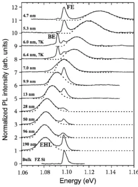
= 190 nm down to lz= 4.7 nm, as reported in Fig. 5.
Spectra reported in this figure show unambiguously that the well-known asymmetrical EHL line centered at 1.081 eV in bulk or thick c-Si QW’s progressively blueshifts when lz
艋15 nm⬇3ax, as a result of the quantum confinement effect
on the carrier band-edge positions. The other lines centered at 1.098 and 1.091 eV originate from FE and bound-exciton 共BE兲 on boron recombination, respectively, either in the QW if lz艌28 nm or in the substrate if the QW turns to be
trans-parent to the laser beam for lz艋13 nm.
An important question arises from the changes in the band diagram of c-Si at low lz: Do we create an incompressible
dimensional EHL or a compressible quasi-two-dimensional EHP? Lowering the quasi-two-dimensionality of the semi-conductor leads to a rise of the valence- and conduction-band degeneracy and to a modification of the carrier masses. This results in serious changes in the kinetic, exchange, and cor-relation terms of the e-h pair energy F共rs兲 and can be an
obstacle for the realization of the minimum-energy condition of F共rs兲 necessary for the e-h system to reach its liquid
equi-librium state. This problem was briefly described in a previ-ous Letter,8but no detailed method or model was presented. Obviously, results of future calculations must show that the 2D EHL or 2D EHP binding energy is greater than the cor-responding exciton binding energy to account for the obser-vation of the condensed phase luminescence. On the con-trary, a larger exciton binding energy would involve the destruction of the condensed phase to the benefit of the ex-citonic phase and would lead to a narrow PL line.
Here, we shall adapt the model of Kleinman21to the case of silicon. Assuming a size reduction of the QW in the共100兲 direction and following Ando and Stern,22 we get g = 2 for the number of populated electron valleys with the greater mass for motion perpendicular to the QW surface. The 2D density-of-states mass is written me= met, where met= 0.19
共Ref. 4兲 is the bulk transversal electron mass. The hole-band degeneracy is raised to 1 with mh−1=
1
2共2mhH兲−1+
3
2共2mhL兲−1
⬇共0.19兲−1,23the inverse of the 2D density-of-states mass of holes, mhH= 0.523 and mhL= 0.154 共Ref. 4兲 the heavy- and
light-hole masses in the bulk material, respectively.
In the frame of the Kleinman’s theory, the screened Cou-lomb potential v共rs2D兲 varies with lz through a
thickness-dependent screening parameter␥共lz兲 and we have
FIG. 5. Solid curves: continuous-wave PL specta acquired on variable-thickness c-Si QW’s forP=6.5 Wcm−2and T = 15 or 7 K. Dotted curves: 3D共lz艌28 nm兲 and 2D 共lz艋13 nm兲 fits performed
v共rs2D兲 = ± 2
1 − exp关−␥共lz兲rs
2D兴 rs
2D , 共6兲
where v and rs2D are expressed in 2D Rydberg and Bohr radius units, respectively. When applied to our QW, these units read ax2D=共4⑀0⑀Siប2/ e2兲关mh−1+ me−1兴⬇6.4 nm and
Ry2D= e2/ 8⑀ 0⑀Siax
2D⬇9.9 meV.
For silicon, the␥ function is deduced from the scale re-lation lz Si = ax 2D共Si兲 ax 2D共GaAs兲lz GaAs共 ␥兲, 共7兲
thanks to the established ␥共lz兲 function given for GaAs in
Table I of Ref. 21.
A more accurate description of the many-body phenom-ena in the QW’s must include the effect of image charges on the strength of the e-h interactions due to the great dielectric mismatch between Si and SiO2. The potential energy vim
resulting from the interaction between a carrier and its image charge, both symmetrically localized with respect to the Si/ SiO2interface, is written
兩vim共z兲兩 = 1 4⑀0⑀Si ⑀Si−⑀SiO2 ⑀Si+⑀SiO2 e2 2z, 共8兲
in SI units, with⑀Si= 11.4⬎⑀SiO2= 3.9. As an example, taking
a carrier in the middle of a 5-nm QW allows us to give the order of magnitude of the “image” contribution 兩vim兩
⬇12 meV with respect to the nonperturbed “Kleinman” po-tential v共rs3D⬇0.86兲⬇29.9 meV 共rs3D⬇0.86 corresponding to the 3D liquid equilibrium density兲. In view of these val-ues, SOI QW’s appear as unique samples in which effects of image charges are expected to play an important role on the electronic and optical properties.
In order to take account of the influence of image charges in the potential of QW carriers, we use the theory of Keldysh24,25 which gives the l
z dependence of the exciton
binding energy BEX共lz兲 in planar semiconductor-dielectric
nanostructures: BEX共lz兲 = e2 4⑀0⑀Silz
冋
ln冉
⑀Si 2 ⑀SiO2 2 lz ax 3D冊
− C册
for ⑀SiO2 2 ⑀Si 2 ax 3D⬍ l z⬍ ax 3D , 共9兲 BEX共lz兲 = e2 4⑀0⑀Silz冋
ln冉
⑀Si 2 ⑀SiO2 2冑冉
lz ax3D冊
2 + 42Ex 3D Eg冊
− C册
for lz⬍ ⑀SiO2 2 ⑀Si2 ax 3D , 共10兲where C⬇0.577 is the Euler constant, Ex
3D
the bulk exciton binding energy, and Eg= 1.170 eV the bulk band gap at T
= 6 K.
The new screening parameter modified by the image charges is obtained by solving the two-equation system
aris-ing from the variational principle startaris-ing from the
␥-dependant model potential 共6兲 and from a test exciton wave function23
␥= p3/关2共1 + p/2兲2兴, 共11兲
BEX=关2␥/共1 + p/2兲兴 −␥2/p2, 共12兲
when BEXtakes its “image” value for a given lzas given in
Eqs.共9兲 and 共10兲.
The free energy by e-h pair at zero temperature is com-puted numerically and is the sum of the average kinetic en-ergy of a totally degenerate e-h plasma EF=共EF
e
+ EF h兲/2 and
of the exchange and correlation terms EX and EC, as
de-scribed in Ref. 21.
As shown in Fig. 6共a兲, ␥共lz兲 decreases with lz, with or
without including the image charges effect.26 Keeping in mind Eq.共6兲, we deduce that the lowering of the dimension-ality involves an increase in the Coulomb energy per e-h pair
FIG. 6. 共a兲 Screening parameter ␥ as a function of the QW thickness with or without the image charges effect共solid and dotted curves, respectively兲. 共b兲 Free energy as a function of rs for the
5.6-nm QW with or without the image charges effect 共open and solid squares, respectively兲.
at fixed rs2D, which is reinforced by the image charge intro-duction.
The complete calculation of the free energy per e-h pair reported in Fig. 6共b兲 shows that F has a local minimum at the 共r0, EG兲 point, where 兩EG兩 denotes the liquid binding energy,
and that兩EG− BEX兩=⌽⬎0 共⌽ being the exciton work
func-tion兲. This qualitatively justifies the observed spectra in Fig. 5 as originating from a condensed e-h phase and a priori predicts a liquid formation. Moreover, Fig. 6共b兲 clearly shows that image charges are responsible from an increase in 兩EG兩 and in the equilibrium density n0
2D
=共r02Dax
2D兲. This re-sult goes in the same way as the strengthening of the Cou-lomb interaction observed in Fig. 6共a兲 and proves that image charges contribute to the liquid stabilization.
Systematic calculations of the free-energy functions have been performed for various lzin the 4 – 22 nm range with or
without the image charge effect. They indicate an increase of 兩EG兩 and ⌽ with decreasing lz, in agreement with Kleinman’s
results for 共100兲 Ge QW’s,21 and larger numerical values when introducing the image charges, which confirms their stabilizing properties upon the liquid.
No excitonic contribution appears on PL spectra in Fig. 5. This experimental observation could be ascribed to a signifi-cant increase in the exciton work function which would modify the liquid-gas equilibrium and would favor liquid formation at the expense of the exciton gas. As mentioned above, calculations corroborate experiments and tend to show that the 2D liquid binding energy increases more rap-idly than the exciton binding energy as lzis lowered.
Data in Fig. 5 were analyzed with the 3D model function 共1兲 for lz艌28 nm and with the 2D model function
L共h兲 = L0
冕
0 h¯ f共⑀,EF e兲f共h ¯ −⑀,EF h兲d⑀ 共13兲for lz艋13 nm. In Eq. 共13兲, L0is constant and EF e
and EF h
are the 2D e-h Fermi levels given in Ref. 21. The new spectro-scopic band gap Eg
⬘
= h− h¯ must include the effects of thequantum confinement energy on the band-edge positions and the changes in the band-gap renormalization energy induced by the modification of the exchange-correlation energy Fxc共rs
2D兲 in the low-dimensional e-h system. Several works concerning calculations of the quantum confinement energies in c-Si nanostructures are reported in the literature.27,28Here, we shall use the ab initio calculations of Niquet et al.29 which give the quantum confinement energy in 共100兲 c-Si QW’s as a function of lz. The fits of these calculated values
give for the valence- and conduction-band edge positions
Ev共lz兲 = Kv lz 2 + avlz+ bv , 共14兲 Ec共lz兲 = Kc lz2+ aclz+ bc + Eg, 共15兲 where lzis in nm, Kv= −1326.2 meV nm2, av= 1.418 nm, bv = 0.296 nm2, K c= 394.5 meV nm2, ac= 0.939 nm, and bc
= 0.324 nm2. For a given thickness,⌬E
BGRis computed
nu-merically from the Fxc function following Eq. 共34兲 in Ref.
21. Finally, for fitting, the rs
2D
-dependent spectroscopic gap, introduced in Eq.共13兲 is written
Eg
⬘
= Ec− Ev+⌬EBGR−បTO. 共16兲Results of 2D fits are reported in Fig. 7 in bulk units. For more convenience in interpreting the results, we have calcu-lated the critical interparticle spacing parameter at the liquid-plasma transition temperature Tcin the explored lzdomain. A
crude estimate of Tc can be made by examining the
temperature-dependent energy function E per e-h pair. In complete analogy with the 3D case,15we can set E共n2D, T兲 as the sum of the free energy at zero temperature and of a T term linked to the 2D plasma specific heat, and we have
E共n2D,T兲 = F共n2D兲 −
6n2Dប2共kBT兲2共mh+ gme兲 共17兲
in SI units. The critical temperature is reached when E共n2D, T兲 has no more local minimum.30
Experimental densities are found to be within the “liquid” domain located between the squares and circles共cf. Fig. 7兲, when image charges are introduced in the calculations. Nu-merical values of the pair density are found to be in the 1 – 2⫻1012cm−2range. If we only take into account the non-perturbed Kleinman potential 共6兲, we find that the experi-mental densities are outside the liquid domain and have larger values than the calculated liquid equilibrium density, which has no physical significance. The comparison between experience and calculus shows that the spectra recorded for the 4 – 13 nm QW’s are well explained by carrier recombina-tion in a 2D EHL.
In view of the simplicity of the model, more accurate calculations must be carried out and compared to our data. In particular, great care must be given to the form of the screened Coulomb potential in varying-thickness QW’s with low lz. The influence of image charges on this potential is
also of importance. That is why a complete calculation of the kinetic and exchange-correlation energies with image
FIG. 7. Experimental densities of the 2D e-h system共triangles兲, as deduced from fits performed on spectra in Fig. 5, calculated interparticle spacing parameters at zero temperature共squares兲, and
charges at the Si/ SiO2 interfaces must be attempted from first principles using a nonscreened Coulomb interaction be-tween carriers.
The band degeneracy set to 2 for the electrons and 1 for the holes is another important problem which has to be pointed out and deserves a more sophisticated treatment. The previous degeneracies are only available in the case of very small thickness, due to the complete splitting of the different energy bands of electrons and holes. In the frame of the effective mass theory and taking the case of electrons, one can give a crude estimate of the energetic splitting⌬EQ
be-tween the two groups of electron valleys. Assuming a size reduction of the QW in the共100兲 direction, the first group is twofold degenerate with a mass mz= mel⬇0.92 共Ref. 4兲 for
motion perpendicular to the QW surface, whereas the second group is fourfold degenerate with mz= met⬇0.19 共Ref. 4兲.
We take ⌬EQ= ប2 2
冉
lz冊
2冋
1 met − 1 mel册
. 共18兲The splitting is complete when the inequality ⌬EQ
艌EF
e共n2D兲=ប2n2D/ m
etg is fulfilled and gives the associated
critical thickness lz c 共E
F e
being the 2D Fermi quasilevel as given in Ref. 21兲. Assuming the density varies continuously between thick and narrow QW’s, we can reasonably set n2D/ l z c = n03D⬇3.2⫻1018cm−3, and we find l z c = 9.2 nm. In the intermediate regime, when the band splitting is not yet achieved, several types of recombination are expected: of “hot” type, between the more split valence and conduction bands, of “cold” type, between the less split valence and conduction bands, and also recombination between “hot” and “cold” carriers. The recombination between carriers originat-ing from these two groups of bands would result in a camel’s-back-type spectrum in the intermediate thickness re-gime.
On the other hand, experiments as a function of P in narrow QW’s are necessary to observe the two-dimensional free exciton at very low pumping powers and could be a very efficient way to measure the exciton work function. In such a case, these experiments could lead to check the accuracy of both the exciton and liquid binding energies.
B. Effects of variable injected carrier density in narrow quantum wells
As we did above for the 3D case in the first section, we use the usual variable-P method to determine the nature of the condensed phase in thin QW’s. We can see in Fig. 8共a兲 PL spectra acquired under cw operation on the 4.7-nm QW at fixed temperature共T=6 K兲 and variable P. As shown in Fig. 8共b兲, the line full width at half maximum 共FWHM兲 is inde-pendent of pumping level, neglecting any broadening due to the weak contribution at 1.131 eV. This line is ascribed to the TA replica of bound on boron excitons 共BE’s兲 in the underlying bulk c-Si and negligibly alters the high-energy side of the QW PL spectra at lowP.
This result differs from the 3D case where the change in the spectral shape associated with the Mott transition be-tween the excitons and EHP is much more spectacular.
In-deed, if we look at the 100-nm QW spectra reported in Fig. 1 and acquired above Tc, we can see that the plasma
line-width measured during the Mott transition reduces in a ratio of 1–2 corresponding to the low-density exciton state.
In view of the results reported in Fig. 8共c兲, and consider-ing that the condensate linewidth only depends on the phase density at fixed temperature, we deduce that the intrinsic
FIG. 8. 共a兲 PL spectra acquired on a 4.7-nm QW at 6 K as a function of laser power with P=4⫻103W cm−2 共curve a兲, 26 W cm−2共curve b兲, 13 W cm−2共curve c兲, 6.5 W cm−2共curve d兲,
and 0.7 W cm−2共curve c兲. 共b兲 Full width at half maximum of the
recombination lines shown in共a兲. 共c兲 Filling factor and line position as a function ofP for the 4.7-nm QW.
density of the photocreated e-h phase is constant in the 4.7-nm QW although the mean carrier density varies with P. This clearly demonstrates that the e-h pairs condense into a constant-density liquid state, while the mean carrier density changes with the laser power. This comparison highlights the differences between the thick and thin QW’s and shows the incompressible nature of the e-h fluid created in thin QW’s under the above-mentioned physical conditions.
In contrast with the theory of electron hole liquids in bulk materials, spectra recorded in Fig. 8共a兲 slightly blueshift as P decreases, which is a priori surprising since keeping constant the density does not modify the band-gap renormalization energy ⌬EBGR. Here, we shall present a simple model in
which the 2D EHL droplet coalescence plays an important role in the spectral properties. This 2D model is in complete analogy with the 3D model as discussed in Ref. 8 for the case of the 3D nanodroplets and uses the more “classical” surface energy picture31to give account of the spectral blue-shift.
The QW thickness being of the order of magnitude of the bulk Bohr radius共ax
3D= 4.9 nm兲, the 3D EHL droplets cloud will undergo a change in the spatial carrier distribution in 2D systems towards a flat cloud of EHL pancakes with radius rxy. The energy Exyof a EHL pancake of radius rxy
contain-ing N e-h pairs is written
Exy= NEG
⬘
+ 2rxyi+ 2rxy2
l, 共19兲
where EG
⬘
共N/S兲=Eg+ EG共N/S兲−បTO is the spectroscopic2D liquid ground-state energy depending on the e-h pair den-sity N / S,iis the liquid surface energy per unit surface on
the Si/ SiO2 interface, and l is the line energy per unit
length on the pancake perimeter. Deriving Eq.共19兲 with re-spect to N gives us the pair chemical potential. When evalu-ated at the equilibrium density n02D= N /rxy2, we have
共rxy兲 =共⬁兲 + 2i n02D+ l n02Drxy , 共20兲
where 共⬁兲 denotes the high-energy PL cutoff of infinite-radius pancakes. The two other line and surface terms in Eq. 共20兲 all positively contribute to the total pancake energy and are responsible of the line blueshift in finite-radius pancakes spectra. However, one can see that the surface contribution in the e-h pair chemical potential does not depend on the pan-cake size, which is not surprising since in the case of a 2D geometry the internal pancake energy NEG
⬘
and the surfaceenergy 2iS vary in the same way as rxy
2. In the framework of this model, the experimental shift of the 2D EHL PL lines under variableP is interpreted as a rxy-dependent EHL
pan-cake chemical potential arising from a change in the panpan-cake perimeter and in the line energy.
In the coalescence model, the pancakes radius depends on the filling of the QW in 2D EHL, which can be evaluated in the same fashion as the pair density in thicker QW’s关cf. Eq. 共2兲兴. The filling factor Fliq
2D is defined as the mean pair to liquid densities ratio and is written
Fliq
2D共P兲 =P共1 − R兲A共lz兲
EHL
n02Dh , 共21兲
with n02D⬇2⫻1012cm−2 andEHL⬇200 ns in a 28-nm QW
at 6 K. In Eq.共21兲, we have neglected any carrier diffusion along the QW which would cause a slight deviation of Fliq
towards lower values. This assumption agrees well with the formation of a condensed state of carriers under a liquid form. The filling factor and the line positions are reported in Fig. 8共c兲 as a function of P. Two high- and low-P regimes emerge from the curve shapes, with an intermediate regime showing opposite variations of the two curves. This sets up a clear correlation between the QW filling and the line position and supports our hypothesis on the coalescence. In particular, in the 1⫻103W cm−2power range, F
liq
2D
and the line position reach a saturation value of 100% and 1.121 eV, respectively, which correspond to the complete coalescence of EHL pan-cakes into a macroscopic EHL state and to the subsequent disappearance of the excess line energy. Strictly speaking, Eq. 共21兲 gives values greater than 100% in the high-P range—more precisely of the order of 200%—corresponding to the creation of a uniform EHL layer spreading outside the laser spot area, but we preferred limiting Fliq
2D
to the 关0, 1兴 interval to keep physical significance.
The line energy l can be found by measuring the PL
energetic shift⌬E on spectra corresponding to PL emission by coalesced liquid共high P兲 and EHL pancakes with radius rxy共low P兲. According to Eq. 共20兲, we find ⌬E=l/ n02Drxy,
where the unknown radius rxyneeds to be determined using
the 2D extension of the 3D nanodroplet model.8
Due to many-body interactions leading to the band-gap lowering, 2D EHL pancakes can be viewed as QW’s with barrier heights relative to the outside given by the carrier work functions⌽e=⌽h=⌽/2. Assuming a gradual 2D
para-bolic potential of the form Ve,h共xy兲=
1 2me,heh 2 xy 2 for both electron and hole energy bands, with the condition Ve,h共rxy兲
=⌽e,h=⌽/2, the ground-state energy of a single particle
im-mersed in the pancake is the solution of the 2D harmonic oscillator␦Ee,h=共ប/rxy兲
冑
2⌽e,h/ me,h, with me= mh= 0.19. Thee-h pair excess energy resulting from the quantum confine-ment in small pancakes is identified with the spectroscopic blueshift at lowP, which provides the necessary relation to estimate the pancake radius and finally the line energy. Data give us ⌬E⬇10.7 meV and the related numerical values rxy⬇13.4 nm and l⬇2.9⫻106eV m−1, obtained with
the relations ⌬E=␦Ee+␦Eh and ⌬E=l/ n02Drxy, with
⌽⬇12.8 meV, as given by numerical calulations for the 4.7-nm QW and n02D= 2.0⫻1012cm−2.
This result is in quantitative agreement with the observed 3D nanodroplet radius in a 28-nm QW共Ref. 8兲 set to 14 nm and strongly suggests to us that the characteristic size of a small e-h aggregate continuously passes from a 3D to a 2D geometry without noticeable radius modification. On the other hand, experimental measurements of the surface energy in bulk c-Si共Ref. 32兲 yields= 1.3⫻1013 eV m−2. This term,
when extrapolated to its “unidimensional” value, gives an idea of the estimated line energy l
est⬇
冑
s= 3.6value. These data support the previous EHL pancake model and the assumptions on the coalescence and the influence of the line energy on the recombination spectra.
The EHL pancake model provides the simple “universal” relation for any semiconductor between the line energy, the 2D exciton work function, and the zero-temperature equilib-rium density by equating the theoretical spectral blueshifts given in the two previous approaches—i.e., the line energy and the parabolic potential methods:
l n02D=ប
冑
⌽冉
1冑
me +冑
1 mh冊
. 共22兲Measurements of the pancake radius by means of diffusion experiments would be of great interest to confirm the EHL pancake formation, as Pokrovskii and Svistunova33 did for bulk Ge. This method would give a more accurate value of the line energy by precisely knowing rxyand should be
com-pleted by a laser-power-dependent study of recombination spectra to determine⌽. These experiments would be a test to verify the pancake model relevance by checking the validity of Eq.共22兲.
C. Phase diagrams of carriers in narrow QW’s
Phase diagrams of carriers in QW’s give very important information about e-h condensation properties such as the critical temperature or liquid-gas phase boundaries. Many methods of calculation have been reported in bulk semicon-ductors and give satisfactory results when compared to the data. The “universal” method of the corresponding states of Guggenheim34 based on the similarities of the interparticle potential of various species or the noninteracting droplet fluctuations model of Reinecke and Ying35cannot be adapted to our case. Indeed, in view of the Kleinman’s model, the interparticle potential depends on the thickness and may lead to some shape modifications with respect to the “Guggen-heim” potential at low thickness. Moreover, the lack of the-oretical estimates of the line energy of EHL pancakes make it difficult to adapt the model of Reinecke and Vashishta to the 2D case. A very convenient way to draw up the 2D phase diagram would be to put the two conditions of mechanical and chemical equilibrium between 2D free excitons and 2D EHL.4 In this method, the e-h pair energy needs to be com-puted over a wide range of density for a given thickness, which is an obstacle in the determination of the phase dia-gram.
Here, we use a simple spin-1 lattice-gas model adapted from the 3D approach of Droz and Combescot.36 In our model, the 2D plasma is represented by a 2D square lattice of cells with “spin” Si共+1,−1,0兲 if the ith cell is occupied by
one electron, one hole, or is empty. The Hamiltonian of the two-dimensional e-h system becomes
H =1 2J共x兲具i,j典
兺
SiSj−兺
i Si 2 + Ax兺
i Si 2 , 共23兲where x =N/N0 is the density of occupied cells, with N0 = 2n02D the total carrier density at zero temperature, equal to the number of cells, andN=ne
2D + nh
2D. J共x兲 is the screened
Coulomb potential between two cells, whereas the propor-tionality constant A enters in the density-dependent kinetic term in Eq.共23兲. The Coulomb interaction between one cell and the other ones is limited to the four nearest-neighboring cells. In the mean-field approximation, one obtains the set of equations 共m,x,T兲 = Ax − kBT ln 2共1 − x兲 x − kBT ln
冋
cosh 4mJ共x兲 kBT册
, 共24兲 m = x tanh共4J共x兲m/kBT兲 共0 ⬍ m 艋 1兲, 共25兲for the chemical potential and the spin thermal average at the ith cell.
J共x兲 and A can be estimated by comparing the Hamil-tonian given in Eq.共23兲 to the exchange-correlation and ki-netic energies at zero temperature and n = n02D, respectively. For x = 1, we deduce J共1兲=兩Fxc共n02D兲兩/8 and A=关EF
e共n
0 2D兲 + EFh共n02D兲兴/4. The density dependence of the Coulomb term is assumed to follow a “Kleinman” exponential law—i.e.,
J共x兲 ⬇兩Fxc共n0 2D兲兩 8
冉
1 − exp冋
− ␥共lz兲 ax2D冑
n02Dx册
冊
, 共26兲 ␥ being expressed in ax 2Dunits. The exchange-correlation term Fxcand the quasi-Fermi levels at the equilibrium
den-sity n02Dare found after numerical calculations of the ground-state parameters as described in the previous section, with or without the influence of image charges. The phase diagrams are numerically computed thanks to Eqs.共24兲 and 共25兲 using Maxwell construction. Here, only two parameters are neces-sary to construct the phase diagram of carriers for a given thickness—namely, n02Dand Fxc共n02D兲—knowledge of which as a function of lz makes possible systematic studies as a
function of the thickness.
Results of calculations are reported in Fig. 9 for lz= 2.4,
10.0, and 20.8 nm. Here, image charges are not included in the calculus of the␥function. Each curve separates the
free-FIG. 9. Phase diagrams of carriers calculated with the spin-1 lattice-gas model for various QW thicknesses. The image charge effect has been neglected.
exciton and liquid domains at low and high densities, respec-tively. The critical temperature is given by the highest point on each diagram and terminates the phase separation be-tween a gas of excitons in equilibrium with a liquid and a compressible plasma as T is raised.
Lowering the thickness clearly modifies the shape of the phase diagrams: the critical temperature nearly doubles be-tween 20.8 and 2.4 nm and reaches 69 K, well above its bulk value of 28 K, and the zero-temperature equilibrium density increases. This behavior originates from the rise in the 2D EHL binding energy at low thickness as deduced from pre-vious calculations, resulting in a more vigorous increase in the exchange-correlation term J共1兲 than in the kinetic term A as lz is lowered. Thus, at low thickness, the extra kinetic
energy due to the strong carrier localization is balanced by a more efficient stabilizing exchange-correlation energy, mak-ing the liquid stable up to elevated temperatures. This result is in the spirit of the universal relation observed in many bulk semiconductors between the liquid ground-state energy 兩EG兩 and the critical temperature Tc 共Ref. 37兲—i.e.,
kBTc/兩EG兩⬇10%. Concerning narrow QW’s, numerical
esti-mates give constant values around 13%, which is very close to the bulk term and seems to indicate that the “bulk” rela-tion is also valid in two dimensions.
Another important point related to the shape of the grams has to be addressed. The low-density sides of the dia-grams in Fig. 9 show that at low temperature—i.e., out of the critical region—the exciton condensation density increases with lzat constant temperature. This result is the signature in
the diagram of the rise of the exciton work function when lz
decreases, as calculated in the previous section. The present phase diagram calculus is a supplementary indication that the 2D FE line is expected to vanish in very narrow c-Si QW’s. Although the spin-1 lattice-gas model is very simple, it brought very satisfactory results when applied to the case of bulk Ge共Ref. 36兲 and provided reevaluated theoretical phase diagrams in remarkable agreement with the experience after fitting of A and J共1兲. However, in view of the sensitivity of
the model to the A and J共1兲 variations and of the uncertainty of the liquid ground-state parameter calculations, previous results concerning the phase diagrams should merely be in-terpreted qualitatively. Experimental determination of the phase diagram of a 2D e-h system would be of great interest, as the study of the influence of the thickness on the Tc
varia-tions, for instance.
V. CONCLUSION
Silicon QW’s offer the unique opportunity to reinvestigate e-h condensation processes in confined media. Evidence has been reported for the formation of the exciton and electron-hole liquid-plasma phases in SOI QW’s over a wide range of thickness, from 190 nm down to 4.7 nm. Several regimes have been identified, according to the range of thickness.
For the thickest wells共lz艌15 nm兲, observation of
steady-state and dynamical effects shows the crucial influence of the structural SiO2barriers on e-h condensation properties.
In the weak quantum confinement regime 共lz艋15 nm兲,
evidence of the formation of an e-h condensed phase—a liq-uid and incompressible phase—under quantum confinement in c-Si QW’s is made. In view of the simplicity of the model used here to analyze the data, some complementary calcula-tions should be carried out to accurately compute the ground state of the two-dimensional EHL. In particular, great care should be taken by including the influence of image charges in the model. Comparison between experimental data and a more sophisticated theory could give very precious informa-tion on the magnitude of the contribuinforma-tion of these charges in the potential of carriers in the QW. We would like to point out that the experimental measurement of the phase diagrams of carriers in varying-lz QW’s is of importance since
com-parison between results of the many-body theories and data—equilibrium density and critical temperature—is straightforward. This later point requires extensive work but is necessary for further investigations of the two-dimensional electron-hole liquid.
*Present address: Université de Sherbrooke, département de génie électrique et génie informatique, 2500 boulevard de l’université, J1K 2R1, Sherbrooke, Québec, Canada. Electronic address: nicolas.pauc@usherbrooke.ca
†Electronic address: calvo@drfmc.ceng.cea.fr 1J. R. Haynes, Phys. Rev. Lett. 17, 860共1966兲.
2L. Keldysh, in Proceedings of the 9th International Conference
on the Physics of Semiconductors, Moscow, 1968, edited by S.
M. Rivkin and Yu. V. Shmartser 共Nauka, Moscow, 1968兲, p. 1307.
3V. M. Asnin and A. A. Rogachev, JETP Lett. 7, 360共1968兲. 4T. M. Rice, J. C. Hensel, T. G. Phillips, and G. A. Thomas, in
Solid State Physics, edited by H. Ehrenreich, F. Seitz, and D.
Turnbull共Academic Press, New York, 1977兲, Vol. 32.
5M. Bruel, Nucl. Instrum. Methods Phys. Res. B 108, 313共1996兲. 6B. M. Bruel and A. J. Auberton-Herv, Jpn. J. Appl. Phys., Part 1
36, 1636共1997兲.
7M. Tajima and S. Ibuka, J. Appl. Phys. 84, 2224共1998兲. 8N. Pauc, V. Calvo, J. Eymery, F. Fournel, and N. Magnea, Phys.
Rev. Lett. 92, 236802共2004兲.
9S. Nihonyanagi and Y. Kanemitsu, Appl. Phys. Lett. 85, 5721
共2004兲.
10D. E. Aspnes, in Properties of Crystalline Silicon, edited by R.
Hull共Inspec, London, 1999兲.
11T. M. Rice, Nuovo Cimento Soc. Ital. Fis., B 23, 226共1974兲. 12P. Vashishta and R. K. Kalia, Phys. Rev. B 25, 6492共1982兲. 13R. B. Hammond, T. C. McGill, and J. W. Mayer, Phys. Rev. B
13, 3566共1976兲.
14Handbook of Mathematical Functions, edited by M. Abramowitz
and I. A. Stegun共Dover, New York, 1964兲.
15M. Combescot, Phys. Rev. Lett. 32, 15共1974兲.
16A. F. Dite, V. D. Kulakovskii, and V. B. Timofeev, Sov. Phys.
JETP 45, 604共1977兲.
1497共1977兲.
18L. M. Smith and J. P. Wolfe, Phys. Rev. B 51, 7521共1995兲. 19I. Balslev, Phys. Status Solidi B 101, 749共1980兲.
20J. Weber, in Properties of Crystalline Silicon, edited by R. Hull
共Inspec, London, 1999兲.
21D. A. Kleinman, Phys. Rev. B 33, 2540共1986兲.
22A. T. Ando and F. Stern, Rev. Mod. Phys. 54, 437共1982兲. 23D. A. Kleinman, Phys. Rev. B 28, 871共1983兲.
24L. V. Keldysh, JETP Lett. 29, 658共1979兲. 25L. Keldysh, Phys. Status Solidi A 164, 3共1997兲. 26The␥共l
z兲 function taking account of the image charge effect has
been calculated using Eq. 共9兲, assuming a total validity of
BEX共lz兲 in the whole range of thickness of Fig. 6共a兲.
27H. Kageshima, Surf. Sci. 357-358, 312共1996兲.
28S. B. Zhang and A. Zunger, Appl. Phys. Lett. 63, 1399共1993兲. 29Y. M. Niquet, C. Delerue, G. Allan, and M. Lannoo, Phys. Rev. B
62, 5109共2000兲.
30Strictly speaking, this condition for the minimization of E共n2D, T兲
should be replaced by the two simultaneous conditions
on the chemical potential —i.e., 共n2D, T兲/n2D =2共n2D, T兲/n2D 2= 0, with 共n2D, T兲=n2DE共n2D, T兲/n2D.
The T term in Eq.共17兲 leads to a zero contribution in the derivatives and should be developed at higher orders to give account for any influence of the temperature on the deriva-tives. However, in view of the similar values obtained for Tcin
the bulk c-Si by using the two methods共Ref. 4兲, we shall con-sider that our approximation is valid and gives satisfactory nu-merical values.
31B. Etienne, C. Benot la Guillaume, and M. Voos, Phys. Rev. Lett. 35, 536共1975兲.
32P. Voisin, B. Etienne, and M. Voos, Phys. Rev. Lett. 42, 526
共1979兲.
33Ya. E. Pokrovskii and K. I. Svistunova, JETP Lett. 13, 212
共1971兲.
34E. A. Guggenheim, J. Chem. Phys. 13, 253共1945兲.
35T. L. Reinecke and S. C. Ying, Phys. Rev. Lett. 35, 311共1975兲. 36M. Droz and M. Combescot, Phys. Lett. 51A, 473共1975兲. 37T. L. Reinecke and S. C. Ying, Phys. Rev. Lett. 43, 1054共1979兲.