BASIC MODULE FOR AN INTEGRATED OPTICAL
PHASE DIFFERENCE MEASURMENT AND
CORRECTION SYSTEM
by
Boris Golubovic
S.B. E.E., Massachusetts Institute of Technology (1991) S.B. Physics, Massachusetts Institute of Technology (1990)
Submitted to the Department of
Electrical Engineering and Computer Science in Partial Fulfillment of the Requirement for the
Degree of Master of Science
in
Electrical Engineering and Computer Science
at the
Massachusetts Institute of Technology
September 1993
© Massachusetts Institute of Technology 1993 All Rights Reserved
-• /2 //
Signature of Author
Certified by
Accepted by
S
Depart;yent of Electrical Engineering and Computer Science
/
September 30, 1993Robert H. Rediker
Thesis Advisor
.. i Frederic R. Morgenthaler
Mu't, irman, Department Committee on Graduate Studies
BASIC MODULE FOR AN INTEGRATED OPTICAL PHASE DIFFERENCE MEASURMENT AND CORRECTION SYSTEM
by
Boris Golubovic
Submitted to the Department of Electrical Engineering and Computer Science on September 30, 1993 in partial fulfillment of the requirements for the degree of
Master of Science in Electrical Engineering and Computer Science Abstract
A basic module for an integrated optical phase difference measurement and
correction system was developed and fabricated in the GaAs-AlGaAs material system. The implemented device made it possible to measure the relative phase difference between two waveguides using a small fraction of the power (<10%) for diagnostic purposes. This proof-of-concept device incorporated waveguides, waveguide couplers and Y-junctions, phase modulators, and photodetectors on the same substrate. This thesis describes the design, fabrication and operation of the implemented device. Waveguide phase modulators with Vx=5.0V for =-0.865gm were fabricated. Selective Be ion implantation and rapid thermal annealing was used to form the p+-n--n+ modulator structure. The phase was
modulated via the linear electrooptic effect in the reverse-biased p+-n--n+ structure.
A Y-junction interferometer was used to obtain the relative phase difference between the two waveguides. Integrated MSM photodetectors, 17x69gm in size, with TIR mirror coupling were used for signal detection. Both, the interferometer and detector were fabricated and operated between two, 30gtm separated waveguides. A phase dither detection system made it possible to determine the relative phase between two waveguides largely independent of the power ratio between the individual guides.
Thesis Advisor: Dr. Robert H. Rediker
Acknowledgments
I would like to thank my thesis advisor, Dr. Robert Rediker, for giving me the opportunity to do this research, and all the advice which went well beyond the scope of this thesis. I am grateful to Joe Donnelly for all his time, guidance, and encouragement during this thesis work. I have learned a great deal from him.
The AlGaAs material grown by Chris Wang, and Bill Goodhue's etching system were instrumental in the successful completion of this thesis. I would like to thank everyone in the Electrooptic Devices Group at Lincoln Laboratory, especially Bob Bailey and John Woodhouse, for their time and help in fabricating the devices for this thesis.
I am also thankful to my family and friends for their encouragement and support throughout the years.
Contents
1 Introduction
9
1.1 B ackgrou n d ... ... 9
1.2 Basic Module for an Integrated Optical Phase Difference Measurement and Correction System... ... 10
1.2.1 Dither Phase Difference Measurement Technique ... 11
1.2.2 System Requirements for Combining GaAs-AlGaAs Integrated Optics and Electronic Circuitry... ... 13
1.3 T h esis O u tlin e ... 14
2 Modeling and Design of Integrated Semiconductor Optical
Components
17
2.1 Modeling of Dielectric Optical Waveguides ... 172.1.1 Dielectric-loaded Strip W aveguides ... 17
2.1.2 The Effective Index Method... ... 18
2.1.3 Optical Loss in Dielectric Waveguides ... ... 24
2.1.4 Index of Refraction in GaAs-AlxGal_xAs ... 26
2.1.5 Waveguide Design and Modal Characteristics ... 26
2.2 Modeling of Dielectric Waveguide Couplers... ... 29
2.2.1 Coupled-Mode Theory Coupler Analysis ... 30
2.2.2 Evaluating the Coupling Coefficient K ... 33
2.2.3 Waveguide Coupler Design... ... 34
2.3 Phase Modulators ... 37
2.3.1 Linear Electrooptic Effect in Zinc Blende 43m Crystals ... 40
2.3.2 Phase Modulator Refractive Index Profile... ... 42
2.3.3 Phase M odulator Design... . ... 44
2.4 Integrated Photodetectors ... ....46
2.4.1 Rectifying Metal-Semiconductor Junctions ... 47
2.4.2 MSM Photodetector with TIR Coupling ... 49
2.4.3 D etector D esign ...51
3 Fabrication of the Integrated Optical Phase Difference
Measurement and Correction System
53
3.1 Device Fabrication ... 533.1.1 Photodetector Definition ... 54
3.1.2 Phase Modulator Definition (Be+ Implantation) ... 55
3.1.3 Waveguide Patterning and Etching ... .. 56
3.1.5 Detector and Phase Modulator Contact Deposition ... 59
3.1.6 Contact Pad Deposition... 59
3.1.7 Backside Processing ... 59
3.2 Photolithographic M ask Set ... ... 60
3.3 Fabricated Optical Phase Measurement and Correction Device ... 62
4 Integrated Optics and Opto-Electronics Evaluation and
Measurement System
65
4.1 O ptical C om ponents... ... 654.2 Experimental Set-up for Evaluating Phase Measurement and C orrection D evices ... ... 68
5 Device Characterization Measurements
71
5.1 Waveguide Phase Difference Measurement ... 715.2 Integrated Photodetector Operation ... 74
5.3 Waveguide Phase Difference Measurement with an Integrated P h otod etector ... ... 80
6 Conclusion
85
6.1 Su m m ary ... ... 856.2 Fu tu re W ork ... ... 86
A Five-Layer Slab Waveguide
87
B Normal Modes of Two-Guide Couplers
91
C Device Processing Recipes
93
1 Introduction
1.1 Background
Integrated guided-wave optical devices have many advantages for the analog processing of optical wavefronts. The benefits include small size, no moving parts, high-speed, reliability, and reproducibility in fabrication. An integrated optical phase front correcting device could be used in numerous applications which include: removing optical phase distortions for imaging applications, phasing the output of laser arrays, or setting the phase between a number of optical waveguides.
In general, a phase front correcting device consists of a set-up which measures the phase variations in the wavefront (at the device input), and a phase corrector for removing of these phase variations. Wavefront phase correctors were implemented using both transmissive devices, employing acoustooptical or electrooptical effects, and reflective devices, such as segment mirrors, monolithic piezoelectric mirrors, continuous thin-plate mirrors, and membrane mirrors. At the present time, reflective devices are the most successfully implemented wavefront correcting devices. In such devices, the phase is corrected by using a variety of substrate material and methods for deforming the mirror surface and thus changing the optical path length over the input wavefront. The design of the active mirror and the drive circuitry depend on the spatial and temporal requirements of the specific application. Active mirrors can be made of discrete segments with individual piston and tilt controls; or they may have a continuously deformable surface attached to an array of piston-action actuators (typically made from a piezoelectric material) which control the mirror deformations. Active control mirrors were successfully implemented for correcting effects of atmospheric turbulence in astronomical optical systems [1].
The design of a wavefront correcting devices used in real-time phase correction systems must consider the requirements set by the specific application such as: required spatial resolution, acceptable phase errors, the intensity variations over the input wavefront, and the response time of the phase correcting system. At this time most wavefront phase measurement systems use one of two approaches for determining the point to point phase difference of a measured wavefront. For the case of coherent sources the phase at each point can be
compared to a phase reference signal and corrected accordingly. In general, if it is assumed that the radiation is locally coherent, the slope of the phase at each point can be determined, and subsequently used to reconstruct the wavefront itself. Frequently used methods for phase measurement include phase-shifting interferometry [2]-[6], the use of a Hartmann sensor [7]-[10], and lateral shearing interferometry [11].
Rediker et al. [12]-[13] have demonstrated an integrated optical guided-wave
system for wavefront sensing. An array of guided-wave elements for wavefront sensing was implemented in lithium niobate, LiNbO3. In this wavefront sensor,
spatial variations in intensity and phase were recorded by an array of alternate straight waveguides and Y-junction interferometers. The detectors at the ends of the straight waveguides measured the intensity, whereas detectors at the Y-junctions were used to record the phase. The optical output power P, of the nth interferometer was given by
P Pen -[P+P 2 1 [Pn n+1 + 2 nPP n n+1 cos ) ] nB (1.1)
where P, and P,+1 are the powers at the outputs of the two adjacent waveguides,
4,
is the phase difference between the two interferometer arms at the Y-junction, and
Bn takes into account losses due to bends and branches.
The small-size and high-speed potential make integrated guided-wave devices particularly attractive for the implementation of phase front correcting devices. The GaAs-AlGaAs material technology is well developed for use in fabricating integrated optical devices operating at wavelengths around 0.85gm (and above). Thus, when combined with integrated electronic control circuits an all integrated wavefront correcting device can be implemented.
1.2 Basic Module for an Integrated Optical Phase
Difference Measurement and Correction System
The basic module for use at GaAs wavelengths that incorporates phase measurement and correction in the same integrated optical device is shown as a part of a larger system in Figure 1-1. The input and output can be coupled to other devices via waveguides, or to free-space by the means of integrated optical antennas [14]-[15]. A small fraction of the power from the straight-trough waveguide is (evanescently) coupled into an interferometer to measure the phase
used to determine the actual phase difference and calculate appropriate phase correcting voltages. The feedback electronics makes it possible to control the integrated phase modulators on the straight-trough waveguides, thus correct any phase distortions in the input wavefront.
FEEDBACK CALCULATE
CONTROL
SYSTEM
VN-1. ..I I
I
D
I
I
I
DETECTO
-D
I
PHASE MODULATOR WAVEGUIDE COUPLER WAVEGUIDE IFigure 1-1: Section of an integrated wavefront correcting device. The highlighted part defines the basic module for phase difference measurement and correction. An actual phase front correcting device would consist of a large number of basic modules (>100).
This thesis had for the goal the proof-of-concept that a basic module that can be implemented as a single integrated optical device. The project required the modeling, design, and fabrication of low-loss AlGaAs guided-wave components including waveguides, bends, Y-junctions, couplers, modulators, and detectors. The device was designed for use with a dither interferometer technique such that phase measurements could be performed independent of the power and power ratio in the two interferometer arms [17].
1.2.1 Dither Phase Difference Measurement Technique
The interferometer technique used for determining the optical phase is similar to dither techniques used in optical fiber sensors [18]-[19], and phase-locked interferometry [20]-[21]. For this purpose an additional phase modulator
was incorporated into one of the Y-junction interferometer arms. If a sinusoidal phase change is applied to one interferometer arm (see Figure 1-2), the power at the detector is given by
Pout = E 2+ E2 2+ 2E1E2cos (AQ~- Fsinot) (1.2)
where E, and E, are the fields in the interferometer arms and the A0 is the phase difference between the two arms. The cosine term in Equation (1.2) can be rewritten
cos (A0 - Fsin0t) = cosAQcos (Fsinot) + sinAosin (Fsin0t) and the time dependent terms can be expanded using Bessel functions
(1.3)
cos (Fsin ot) =
sin (Fsin0t) = J0(F) + 2 J2k(F) cos [2kwt] k=0 2 _ J2k+ l(F)sin [ (2k- 1) ot] k=O Vrsinot
Fr=Vr/Vn
E2ejA# WAVEGUIDE WAVEGUIDE COUPLERFigure 1-2: Interferometer with a dither modulator makes phase difference measurements independent of the power and power ratio in the interferometer arms possible.
Thus, if the signal in Equation (1.2) is passed though a pair of lock-in amplifiers set for the frequencies w and 2o (bad-pass filters at o and 2o), the output amplitudes are described as follows:
A(w) = 2E, EJ ,(F)sinA0 (1.6)
A(2w) = 2E1E2J2(F)cosA(
(1.4)
(1.5)
where J(TF) and J2(F) are Bessel functions of the first kind of order 1 and 2
respectively. Then the expression for the phase difference obtained from Equations (1.6) and (1.7) becomes
-- ~--+..
A
=arc tan A(o)
J2(F) =arctan A()
8 96
(1.8)
AA(2)
Ji(Tj)
A(
2
0
)
r
F 3
.L
2
16
The number of terms required for evaluating the Bessel function is determined by the magnitude of the phase dither amplitude F. Moreover, the expression for the phase difference is independent of the power in the individual interferometer arms. The respective signs of the measured amplitudes A(o) and A(2m) are used to uniquely determine the quadrant of the phase difference A0.
1.2.2 System Requirements for Combining GaAs-AlGaAs
Integrated Optics and Electronic Circuitry
For this research the proof-of-concept devices were operated with of-chip control electronics. The long-term goal of this project, however, is to incorporate the optics, as well as the electronic circuitry on the same chip. Thus care was take to ensure compatibility with the goal of monolithic integration in the future. The principal circuit requirements for implementing the phase measurement and correction system include the following:
* Sample and hold circuits to measure the amplitudes of the first and second harmonic of the dither frequency * A oscillator for the dither frequency, and a frequency
doubler to generate a reference for synchronous detection of the second harmonic
* A divider, arctan, and quadrant detection circuits for calculating the phase difference.
The complexity of the actual electronic circuit designs depends on the required accuracy of the phase measurement and correction system, and the desired speed of operation.
There are two major approaches to combined integration of the optics and electronics. Both, the optical and electronic components can be fabricated in the GaAs-AlGaAs material system. There is no fundamental obstacle to the fabrication of all the electronic circuitry in GaAs. However, since the technology
z
zL
I-O
PHASE WAVEGUIDE WAVEGUIDE MODULATOR COUPLER
Figure 1-3: Basic module for a phase measurement and correction system. V ,,,,, is used to control the relative phase, whereas V,,, can be used to induce an intentional phase imbalance when testing the device.
for fabricating GaAs electronic devices is less mature than for Silicon based devices, a hybrid technology is of interest. Hybrid techniques take advantage of the mature silicon fabrication technology to implement the necessary electronics, whereas GaAs materials can be used to fabricate the desired optical devices. In this integration scheme the GaAs-AlGaAs epitaxial layers would be grown on silicon substrates [22]. The silicon electronic devices can be fabricated first using commercial processing facilities. This is followed by the growth of the GaAs-AlGaAs epitaxial layers and the fabrication of the optical components. Work on hybrid devices for integrating silicon based electronics and GaAs optical devices is presently conducted by Prof. Fonstad at MIT.
1.3 Thesis Outline
This thesis is the continuation of the work conducted by Suzanne Lau [17] with the ultimate goal to fabricate an all-integrated optical phase front correcting device. Suzanne Lau in her work demonstrated that an integrated Mach-Zender interferometer can measure the relative phase between the two interferometer arms. The measured phase was independent of the power imbalance between the
two interferometer arms, and could be dynamically corrected by applying a voltage to the integrated phase modulators.
This work build on the results obtained by Suzanne Lau and further explored additional aspects of implementing an all-integrated optical phase correcting system. This thesis demonstrated the ability of measuring the phase between two waveguides by using a small portion of the power in each waveguide for the phase measurement. In this aspect an external detector was used to record the test interference signal used for evaluating the phase difference. Following this an integrated photodetector, fully compatible with the waveguide components and modulators, was successfully implemented and tested. Finally, the waveguide phase measurement setup was combined with the integrated detector and a phase measurement was successfully demonstrated using only integrated optical components.
2 Modeling and Design of Integrated
Semiconductor Optical Components
2.1 Modeling of Dielectric Optical Waveguides
Dielectric optical waveguides are the basis of the field of integrated optics. Thus the first step to the implementation of an integrated optical device is the design of a structure which can confine and guide electromagnetic radiation -light. The confinement of light in one direction can be achieved by simply taking advantage of dielectric slab waveguides. However, for integrated optical applications it is necessary to confine the light in both the lateral, as well as the vertical direction. Waveguide structures of this kind are commonly referred to as
channel waveguides. A few examples of such structures are show in Figure 2-1. The
choice of a particular waveguide structure depends on its application, as well as the desired device characteristics, materials used, and ease of fabrication.
nE
n2 > 1 (a) n. n2> n1, n3 (c) n, n3 n2 > ni, n3 (b) ni n. 4 n3 > (n2, n4) > n1 (d)Figure 2-1: Cross sections of channel waveguide structures: (a) buried guide, (b) embedded strip guide, (c) rib guide, (d) loaded strip guide.
2.1.1 Dielectric-loaded Strip Waveguides
The dielectric-loaded strip waveguide design, shown schematically in
achieved with the 4-layer dielectric nature of this structure. On the other hand, the lateral confinement of the optical mode, y-direction, is the result of the rib in the upper cladding. In such a structure, the thickness of the waveguide layer, and the rib height, determine the degree of lateral confinement and as such the propagation constant of the guided optical mode. When fabricating this structure it is important that one choose a fabrication technique which allows precise rib height control. Moreover, the thickness of the lower cladding must be sufficient so that a 4-layer slab analysis can be applied in the x-direction.
The exact analysis and calculation of the mode propagation constant in a dielectric-loaded strip waveguide is quite difficult, and only possible using numerical methods. However, for most applications one can resort to approximate methods which yield results in close agreement with the ones obtained using more exact methods. ni v,
3
d P ~I V) Top Cladding Upper Cladding Waveguide Lower CladdingEffective Index Method
I I
-J
L<f (c1
y~
Figure 2-2: Schematic of a dielectric-loaded strip waveguide.
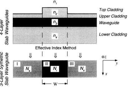
2.1.2 The Effective Index Method
The effective-index method (EIM) is one of the most commonly used methods for analyzing channel waveguides. This method has proven itself by producing results which are in close agreement with more exact computer results, as well as experimental results for a considerable number of practical guide structures [23].
The effective index method allows us to reduce the dielectric loaded ridge waveguide, to a simpler 3-layer symmetric waveguide. The dielectric loaded-strip
waveguide can be divided into three regions consisting of four dielectric layers each. If we treat each of these regions independently, and assume that the layers are of infinite extent in the y-direction, we obtain a set of three four-layer dielectric slab waveguide problems (since outer two slab regions are identical, so that the problem reduces to only two regions). Thus, we can calculate the effective indices
Ns and N, from the slab mode propagation constants, ~,r=2tNs,r/,. If both slab regions support only a single mode, an unique effective index for each region can be determined, and such loaded-strip waveguide structure will support modes which have only one maximum in the x-direction.
After establishing effective indices for each region, the structure can be modeled as a 3-layer symmetric slab waveguide in the y-z plane (see Figure 2-2). The slabs are of uniform extent in the x-direction with an index Ns in the cladding region, and Nr in the guiding region. The analysis of this effective 3-layer slab structure yields an overall P and lateral propagation constants for the y-direction. Since these channel waveguides are designed for single-mode, quasi-transverse electric (TE) propagation, the electric field is predominantly in the y-direction. Thus, the TE slab boundary conditions are used in evaluating the 4-layer eigenvalues, and the transverse magnetic (TM) slab boundary conditions are used
for the lateral 3-layer guide calculations.
Four-Layer Slab Waveguides
Maxwell's equations for a homogeneous dielectric medium of permittivity
E and permeability g with no free charges present, as well as no current
distributions are: Vx E(r, t) = -gC H(r, t) (2.1) at Vx H(r, t) = -EkE(r, t) (2.2) at V eE(r, t) = 0 (2.3) V gH(r, t) = 0 (2.4)
The general wave equation for the electric field is obtained from Maxwell's equations such that
2
V2 E(r, t) - go E(r, t) = 0 (2.5)
-. 1 W2 2d : n Top Cladding Upper Cladding Waveguide Lower Cladding n3> (n2, n) > n3
Figure 2-3: Four-layer slab waveguide. The structure is uniform in the y-z plane.
Applying our assumption of a planar slab waveguide (of infinite extent in the y-direction), we can eliminate one dimension to the wave equation since it is given that a3/y-=O. For the case of transverse electric (TE) slab modes, where
E(r, t) = E(x, z, t)5, the following relations between the electric and magnetic field can be obtained H = E= E = 0 (2.6) H - E (2.7) x y H = E (2.8) S 0)!laX y
To establish the modes propagating in a four-layer dielectric slab waveguide structure one has to find solutions which satisfy the wave Equation (2.5). Moreover, the boundary conditions require that Ey and Hz be continuous across the layer boundaries. Since p is the same in all the layers, the continuity in
Hz is equivalent to the continuity of aEy/lx. The Equations (2.9)-(2.12) satisfy the wave Equation (2.5) in the applicable regions, and Equations (2.13)-(2.16) are the respective derivatives DEy/lx which are required to be continuous across the dielectric layer boundaries .
Layer 1. E = Al eY (2.9)
Layer 2. E = A2coshy2x + B2sinhy2x (2.10)
Layer 3. Ey = A3coskxu + B3 sinkxu, U = X - (W2 + d) (2.11)
Layer 4. E =A 4e 4 v = x - (W2+ 2d) (2.12) L L L
r
W2aE
Layer 1. - A eYX (2.13)
ax
1DE
Layer 2. - = y2 (A2sinhy2x-B 2coshy2x) (2.14)
aE
Layer 3. -Y = -kx (A3 sinkxu-B 3coskxu) (2.15)
aE
Layer 4. = -y4A e (2.16)
ax 44
The quantities yl, 72, 74 are the field amplitude decay constants in the layers 1,2 and
4, whereas k is the propagation constant in the x-direction of layer 3, and 0 is the propagation constant in the z-direction. The quantities Ti, Y2, Y4, and k are all related as follows: S= (2 -k) 1/2 (2.17) 2 2 1/2 2 2 1/2 72 = - k2) = ko (Nff - n2) (2.18) 1/2 y4 = 2 - k4) (2.19) k = (k2 2 1/2 2 2 1/2 = (k 3- ) = ko (n3 - Neff) (2.20)
where ko=2nt/l and k,=(2rt/k)n, i=1...4, X is the operating wavelength, and Neff is the
effective index of the waveguide structure. By matching the boundary conditions for Ey and aEy/lax, and solving the system of linear equations for the propagation constants, the following eigenvalue equation is obtained:
kx [74 (y2 + 1 tanhy2W2) + y2 (y, + 2tanhy2W2) ]
tan (2kxd) = (2.21)
k2 (y2 + ,ltanhy2 W2) - 2,y4 (y, + 2tanhy2 W2)
Equation (2.21) is a transcendental equation which relates the structure parameters to the propagation constants. Since there is no analytical solution to Equation (2.21), a solution for k can be found only numerically. However, a solution for k exists only if the thickness of the guiding layer (layer 3) is larger than the cutoff thickness of the fundamental mode. This cutoff thickness is given by
I Y2 F 1+ 2tanhy2 W2 )]
tcu - arc tan (2.22)
If the guiding layer is thicker than the cutoff thickness the total number of propagating guided modes, m, can be obtained from the condition,
(m - 1) x
t + k 2d (2.23)
X
Summarizing, by solving Equation (2.21) and using Equation (2.20) one can obtain the propagation constants P for the individual guided modes. Thus if the four-layer structure supports only one guided mode, an unique effective index
NefFPl/ko can be obtained.
Three-Layer Symmetric Slab Waveguides
When calculating the propagating modes in a three-layer slab structure one has to start with the wave equation. For the EIM analysis of the loaded strip waveguide structure, the modes in the three-layer symmetric slab waveguide have to satisfy the transverse magnetic (TM) boundary conditions. Thus, to simplify the analysis, instead of the E-field wave equation the H-field wave equation is used. The general form of the wave equation for the H-field is obtained from Maxwell's equation, and is given by
V2 H(r, t) - Ce d-H(r, t) = 0 (2.24)
dt2
Applying our assumption of a planar slab waveguide (of infinite extent in
Side Region Rib Region Side Region
Nr > Ns
Figure 2-4: Three-layer symmetric slab waveguide. The structure is uniform in the x-z plane. The indices N, and N, are obtained using the effective index method.
the x-direction), we can eliminate one dimension to the wave equation since it is given that a/lx=0. For the case of TM slab modes, where H(r, t) = H(y, z, t)k, the following relations between the electric and magnetic field can be obtained
E = H = H = 0 (2.25)
E - H (2.26)
y x
E = J H
(2.27)
z WOEay x
The boundary conditions require that Hx and Ez be continuous across the layer boundaries. The Equations (2.9)-(2.12) satisfy the wave Equation (2.24) in the applicable regions, and Equations (2.13)-(2.12) are the respective expressions for
Ez=-(j/mE)aHx~/x which are required to be continuous across the dielectric layer boundaries.
Layer I Hx = Aey,(y+ W/2) (2.28)
Layer II H = Ailcosk y (2.29)
Layer III Hx = Aile (y - W/2) (2.30)
-j 7, (Y+ W/2)
LayerI Ez = sAle + W/2) (2.31)
Layer II
E
z=
(
k Acosk y
(2.32)
C
-j
r
)
(y-W/ 2)Layer III Ez = •
IYsAiie
( -W/2) (2.33)The quantity Ys is the field amplitude decay constant in cladding layers I and III, k,
is the propagation constant in the y-direction of layer II, and
P
is the propagation constant in the z-direction. The quantities Ys, k and are all related as follows:2 2 1/2 2 21/2
=s (= - k) = ko (Nff- N) (2.34)
2 1/2 2 N2 1/2
ky = (k2_p
) 2ko (Nr-Ne-ff)
(2.35)
where k0=2Tc/X, k is the operating wavelength, N, and N, are the effective indices of the ridge and side region, and P=2Nej/1k. By matching the boundary conditions for
Hx and E, at y---W/2, and solving the system of linear equations for the
propagation constants, the following eigenvalue equation is obtained:
tank -yW (2.36)
72
N k
r yEquation (2.36) is the transcendental eigenvalue equation which relates the structure parameters to the propagation constants. As with the four-layer
structure a solution can be found only numerically. For the three-layer structure there is no cutoff thickness for the fundamental mode, and there is always at least one guided mode present. The total number of propagating modes, m, corresponds to the condition
(m- 1) < W (2.37)
The propagation constant P obtained as result of the EIM and the three-layer symmetric dielectric guide analysis above, is considered to be the propagation constant of the loaded-strip waveguide structure as a whole. If Equation (2.37) yields an m=l (and the four-layer structures were single mode as well) the structure as a whole is expected to support only one guided mode.
2.1.3 Optical Loss in Dielectric Waveguides
An important consideration when designing dielectric optical waveguides is the amount of propagation loss of the optical mode in a particular structure. In general, losses in semiconductor waveguides can be attributed to absorption, scattering, and radiation.
Losses due to absorption can be of various sources, but in semiconductor waveguides band-edge absorption and free-carrier absorption are of primary concern. Band-edge absorption can be avoided if the material is chosen in such a way that the optical mode has a wavelength which is much longer than the wavelength corresponding to the bandgap. In the GaAs material system an increase in the bandgap can be achieved by choosing a high enough aluminum concentration for the AlxGalxAs waveguide layers: increasing the aluminum concentration increases the bandgap energy and thus decreases the bandgap wavelength. For AlxGal-xAs semiconductors, the bandgap energy (in eV) is related to the composition x (for Ox<<0.4) by [24]
E = 1.424 + 1.245x (2.38)
The presence of free-carriers not only reduces the real part of the dielectric constant, but also increases the absorption of the semiconductor [23]. The free-carrier absorption is proportional to the number of free-free-carriers. Thus, free-free-carrier absorption can be minimized by growing epitaxial waveguide layers of material which is nominally undoped (as close as possible to intrinsic). The waveguide epitaxial structures for this research were grown by organometallic chemical vapor
phase epitaxy (OMVPE) with n=l10 5cm-3 and n=10'6cm-3 for the GaAs and AlGaAs
films respectively.
There are two sources of scattering loss in optical waveguides: volume scattering and surface scattering. Volume scattering is caused by imperfections within the volume of the waveguide. However, in all waveguides of interest, the number and size of imperfections is so small that volume scattering is negligible compared to surface scattering loss. Surface scattering losses are largely due to roughness at boundaries between the dielectric waveguide layers. Moreover, scattering losses are generally higher at boundaries where the refractive index changes An are greater. As a result, the loaded strip waveguides are less susceptible to interface roughness than ridge waveguides (see Figure 2-1). For loaded strip waveguides the fraction of the total optical mode intensity near the semiconductor-air interface (An large) is much smaller, resulting in less scattering loss for the same roughness profile [25]. To reduce scattering losses it is important to fabricate smooth dielectric interface layers, particularly if the An is large.
Optical energy can be lost from the waveguides by radiation, in which case optical energy is emitted into the material surrounding the waveguide without being guided. If the substrate is of larger index of refraction than the adjacent cladding layer, part of the waveguide mode may couple into substrate radiation modes. This type of attenuation can be minimized by reducing the coupling between the waveguide and substrate. This can be achieved by increasing the lower cladding thickness or increasing the vertical mode confinement [26].
Radiation losses occur at waveguide bends, changes in guide dimensions, and guide discontinuities [27] [23]. In fact, the limit on how much a waveguide can change direction per unit length, is set by the maximum acceptable loss for a given device. Since for most integrated optical devices waveguide bending is needed, radiation losses from curved waveguides must be considered in the device design. The waveguide bends have the effect of creating a disparity between the traveling distance of the evanescent mode tails along the inner and outer waveguide sides. This introduces coupling between the guided modes and radiation modes and as such introduces loss. The loss at abrupt bends decreases with increased lateral mode confinement, as well as smaller bend angles (less abrupt direction changes).
2.1.4 Index of Refraction in GaAs-AlxGaj-xAs
The index of refraction of AlxGa_-xAs can be controlled by the percentage of
aluminum in the compound: the refractive index increases as the aluminum content decreases [28] [24]. Casey et al. [28] have measured the refractive index as function of energy for AlxGa_-xAs films with aluminum compositions 0<x<0.38. The refractive index of an AlxGaj-xAs film depends nonlinearly on the aluminum concentration x and the operating wavelength ,. Since the experimentally obtained data are awkward for use in numerical modeling of waveguide structures, an alternate means of determining the refractive index of AlxGal-xAs is widely used.
In numerical modeling of the AlxGa_-xAs structures (05x_0.40), the refractive indices were calculated using the following Sellmeier equation
2 0.97501 2
n = (10.906-2.92x) +0.97501 - 0.002467 (1.41x + 1) X2 (2.39) X2 - (0.52886 - 0.735x)2
Equation (2.39) is an empirical fit to measured data [27] for the refractive index of AlxGa_-xAs as a function of x and k. This model yields refractive indices which differ slightly from the experimental data by Casey at al. However, even though the absolute indices differ somewhat, the difference between films of different compositions are in close agreement. Thus, since the properties of a waveguide are largely dependent on the index differences between dielectric layers, the results of numerical simulations yield accurate estimates of waveguide properties.
2.1.5 Waveguide Design and Modal Characteristics
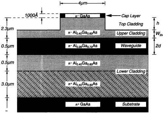
For the purposes of this research the waveguides are designed to propagate only the lowest guided mode. The first step in designing dielectric waveguides is to determine the composition of the individual dielectric slab layers. The dielectric layer structure shown in Figure 2-5 was chosen for this research. This choice of dielectric layers makes it possible to fabricate low loss waveguides for wavelengths around 0.85gm [17]. Moreover, this structure is fully compatible with the fabrication of other integrated optical components needed for this research. The n+ doped lower cladding region is not needed for the waveguide design, but it actually may be causing some guiding loss. However, this layer is required for the implementation of integrated phase modulators discussed in Section 2.3. Once the composition and thicknesses of the individual dielectric layers was chosen, the
device performance was determined by the specific wavelength used, waveguide rib width, and height.
41m ,
7-2.3pmt
0.5pm 0.5pmt
3.OPm+
h w2S 2dFigure 2-5: Dielectric-loaded strip waveguide cross section.
A number of numerical simulations of loaded-strip structures using the
layer composition shown in Figure 2-5 was performed. For single mode operation, the rib width was chosen to be 4Cgm, and was set by the photolithographic mask used for waveguide patterning. This width yields good single mode performance and is large enough to ensure consistent fabrication results. Thus, the only fabrication dependent variable was the actual rib height, which was controlled through the etching process.
The y-direction propagation constant (proportional to the mode confinement) was observed as a function of wavelength X, and W, the side cladding thickness. In Figure 2-6 it can be seen that this particular loaded strip waveguide structure becomes more single mode as the wavelength decreases. This effect is a result of the change in the index of refraction of the individual AlGaAs layers with wavelength, and the change in the mode shapes of the four layer waveguide slabs it affects. As a consequence, the effective index of the side region N, changes faster than that of the rib region N, resulting in smaller mode confinement. Thus, for the loaded strip waveguides structure an increase in excitation wavelength results in a larger cut-off width for the second guided mode.
U. U 0.80 0.70 0.60 0.50 0.40 0.80 0.81 0.82 0.83 0.84 0.85 0.86 0.87 Wavelength [pm]
Figure 2-6: Dependence of the y-direction propagation constant k, on the wavelength.
0.20 0.25 0.30 0.35 0.40 0.45 0.50 0.55
W2s-Upper Cladding Thickness [pm]
Figure 2-7: Dependence of the y-direction propagation constant k, on W2,.
E
0.88 h hh
When fabricating actual waveguides it is of interest how the change in fabrication parameters will affect the waveguide performance. Since the waveguide rib was fabricated by etching off the side regions, it was of interest how the device performance depended on changes in W2. Figure 2-6 shows how the k, depends on W2d at three particular wavelengths for the structure shown in
Figure 2-5. The actual target value for W2, was determined by considering the performance of other integrated optical components used in this project.
2.2 Modeling of Dielectric Waveguide Couplers
Waveguide couplers are integrated optical devices which perform the function of beam-splitters in bulk optics. They make it possible to split the power from one (loaded-strip) waveguide into two or more guides. One of the simplest coupler implementations consists of two parallel waveguides in close proximity to each other. Under these conditions, a fraction of the field in one guide interacts with the adjacent guide resulting in a power transfer. The power transfer is not unidirectional, but the power is exchanged back-and-forth between the guides as often as the length of the device permits it. Full power transfer however, is only possible for guides which have equal propagation constants in isolation. Guides with equal propagation constants are referred to as synchronous waveguides. Equal propagation constants, at all wavelengths, generally occur only when the two adjacent guides are identical. Nevertheless, under specific conditions, for particular wavelengths, it is possible that two dissimilar waveguides are synchronous and full power exchanges are possible [29].
The coupler operation can be described by the interaction of the orthogonal modes of the coupler structure. The waveguide coupler as a whole has a different set of normal modes than the individual waveguides. Thus, the power transfer within the waveguide coupler is described by the propagation of the modes of the coupler structure. If the field at the waveguide input is E(x,y), its propagation can be described in terms of the orthonormal set of guided modes Fi and radiation
modes R(P) of the coupler structure
E(x, y, z) = alFle + a2F2e 2z + ... +f b()R(P))ejpzdp (2.40)
To describe the coupler operation using Equation (2.40) all the guided and radiation modes of the compound structure have to be calculated. In general, it can be assumed that it is too complicated to easily compute all the normal modes
Top Cladding Upper Cladding Waveguide Lower Cladding
Effective Index Method
U
I 41 IjI
JjI
Ijy
x
Figure 2-8: Schematic of a waveguide coupler. Two dielectric-loaded strip waveguides are separated by a distance S. The structure of two adjacent dielectric-loaded strip waveguides is reduced to a one dimensional, five-layer slab waveguide problem.
and their propagation constants. Thus, for many practical applications, the operation of waveguide couplers can be approximately described by the coupled-mode analysis [30].
The couplers used in this project consist of two single-mode waveguides
which are separated by a distance S. The analysis of the structure is started by applying the EIM to reduce the two dimensional loaded strip waveguide to an one dimensional five-layer slab structure. Analogous to the single loaded strip waveguide analysis, TE boundary conditions are applied to solve the vertical four-layer structure to obtain the applicable effective indices. TM boundary conditions are applied for solving the slab coupler in the y-direction.
2.2.1 Coupled-Mode Theory Coupler Analysis
When analyzing waveguide couplers using the coupled-mode formalism, it is assumed that the two guides interact only weakly. The only interaction between the waveguides takes place via their fringe fields. It is assumed that the field at the coupler input, and its propagation, is fully described by the superposition of the lowest even and odd guided mode of the compound structure. Since the input is the superposition of the even and odd modes with different propagation constants,
Pe and o,, the relative phase between them will change as they propagate along z. Thus, if the fields were initially in-phase, they will be out-of-phase at z--t/(Ie-Io).
If at z=0 the total field in the coupler was the sum of the lowest even and odd mode, at z=1 this will correspond to the difference between the two modes. In effect, after an interaction length of L, all the power is transferred from one waveguide to the other. The propagation of the sum and difference fields can be described by two coupled first-order differential equations.
Coupled Equations for the Sum and Difference Fields
The input field at the coupler is the linear superposition of the compound structure modes. The fields G, and G2 are the normalized fields in each of the coupler waveguides, Fe and Fo are the even and odd normal modes respectively. The coefficients which relate G1,2 and F,2 can be defined as follows:
G1 = CFe + c2F° (2.41)
G2 = C3Fe + c4Fo (2.42)
INPUT SECTION WAVEGUIDE COUPLER OUTPUT SECTION
ex
Ty
I I
z=0 EVEN MODE z=L
SINGLE-MODE INPUT OUTPUT INTENSITY
•*
exp(-jiz)
DISTRIBUTION
ODD MODE
• exp(-j,,z)
Figure 2-9: Top view of a synchronous waveguide coupler with a single-mode input waveguide. The input field can be expressed as the superposition of the even and odd mode of the compound coupler structure.
To describe the propagation and changing field pattern, z-dependent coefficients a,(z) and a2(z) for the field patterns G, and G2 have to be introduced.
Moreover, initial amplitude coefficients for Fe and Fo have to be defined. Thus, the propagation of the total field in the waveguide coupler can be expressed as:
Substituting (2.41) and (2.42) into (2.43), and grouping the coefficients for Fe and Fo respectively lead to the relationships
clal(z) + c3a2(z) = b e
c2al(Z)+ c4a2(z) = b2e
-ji*,z
(2.44)
(2.45) To obtain the change of the input fields with respect to z, Equations (2.44) and (2.45) are differentiated with respect to z, and the constants b, and b2are eliminated,
dal da 2 C 1 +C 3 2 dz dz = -jPe (cla + c3a2) (2.46) (2.47) da1 da 2 c2
2dz
- + C4dZ
4 = -o (c2a1 + c 4a2)After solving Equations (2.46) and (2.47) for the da, /dz and da2/dz, the
desired coupled-mode equations are obtained
da, - - iB, a, + K,,a J 1 I z da2 -= -ia + ,, a (2.48) (2.49)
The quantities p3 and P2 are the propagation constants for the two waveguides in isolation, and can be related to the coupler modes as follows
CICIe-C4 C2 3 o C1C4 o-C 2C3fe
1 = ,2 = .
C1 4 c- C2 3
The coupling coefficients K are defined by
C3 C 4 C 1 c2
K12 = - We - o) ' 21 = J . (Po - Pe)
(1 C4 - C2C3
From the Equations (2.48)
C I 4 - C2C3
and (2.49) the general
(2.51)
solutions for the propagating fields in both waveguides can be found to be:
a
1(Z) = [a (0)
a
2(z)
=
ali
(Cs
0Z
+J
P2_P-2P1 sin P0z) + 1 2 -a2 (0)PO
sin sin oz e i z] -iJ [ (01 + I2) /2] zz(2.52)(2 ( 0)
+
1 - 2 .i -ji[ (1 +P2)/2]zCos
POZ
+sin poz e z(2.53)(curo' iji~i
2
o[3
]-
p
2 3
ClC4 - 2c3
(2.50)
2 L 21 l
where
S-
P
2 K2K21 (2.54)The solutions (2.52) and (2.53) give the fields in the coupler waveguides as a function of the input fields, the individual guide propagation constants, and the coupling constants. The field amplitudes in the individual guides oscillate between minimum and maximum values as a result of the beating of the even and odd coupler mode.
In this project the coupler consists of two identical, single-mode
waveguides such that 3,=32. The coupler is used to split the power from one guide
into two such that a,(O)0O and a2(0)=O. This simplifies the general propagation
equations to
al(Z) = al(O)e cos K12z (2.55)
a2(z) = a1(O)e-z sinKl12z (2.56)
2.2.2 Evaluating the Coupling Coefficient ic
The propagation constants of the even and odd modes of a synchronous TM waveguide coupler are calculated in Appendix B. Thus, after the propagation constants are obtained, the coupling coefficient can be found using Equations (2.51). However, since for many practical applications it is difficult to obtain the exact values for 3e and
13,
an alternate method for evaluating ic must be used.From previous assumptions, total field in the coupler is the superposition of the field patterns of the individual guides:
E(y, z) = al(Z)G1 + a2(z)G2 (2.57)
where G, and G2 are the fields of the individual waveguides in isolation. The
power from waveguide 1 is transferred to waveguide 2 by a polarization current
jfP21 generated in waveguide 2 by the evanescent field of guide 1. The coupling
polarization current is, in effect, the change in polarization current due to the presence of waveguide 2 (and its high index region)
The power transferred per unit length, AP, is the overlap between the polarization current and the field in the high index region of waveguide 2 (wg2), and is derived from the Poynting equation:
AP
-
a
2*
G
2(j•o
P
21) da + c.c.
4 wg2
S- • G2* o(N0 2 - N2) a1 Gda + c.c. (2.59)
4
wg2
The power transfer from waveguide 1 to waveguide 2 can also be expressed form the coupled mode Equations (2.48) and (2.49) as
d a2 2 da2 da2 a * a
dz a2 dz dz 2 a2K21 1 2 2 1a1 (2.60)
Thus, by comparing the terms in (2.59) with (2.60), an expression for the coupling coefficient K2 can be obtained to be
21 - j 4 G2* (N2-N2) G da (2.61)
wg2
The same approach yields the expression for K1 2
1 2 = 4o G * (N -N2) Gda (2.62)
wgl
Equations (2.61) and (2.62) are an approximate alternative to Equations (2.51). These approximate expressions relate K to parameters of the two waveguides in isolation and eliminate the need for calculating the modes of the compound coupler structure. Thus, the approximate coupling coefficient for a synchronous TM slab waveguide coupler is obtained by evaluating the overlap integral in (2.61).
(ryk,
)
2
-YS
N
(2.63)
12 =
-i
e2ys, ,r =(12 J + r22 2] p (ryd + 1) s
where y, k, p are the mode constants of the TM waveguide in isolation, 2d the guide width, and S the separation between the adjacent guides.
2.2.3 Waveguide Coupler Design
For fabricating waveguide couplers it is important to understand how the coupling changes as a function of design parameters. Since the coupler is in effect
two waveguides in close proximity, the epitaxial layers used are identical to those used for the single-mode waveguides. Moreover, the width of the individual waveguides was set to be 4gm. Thus the fabrication dependent variables left were the guide separation S, the upper cladding in the side regions W2d, and the actual
interaction length between the two waveguides.
Two sets of devices were designed, each having different coupler parameters. One set of couplers was designed with S=3.4gm, and the other with S=3.6gm. Once the waveguide width and separation are fixed, the coupling between the waveguides becomes a function of W2d. Figure 2-10 shows how the
coupling length (needed to transfer all the power from one waveguide into the other) depends on W,. However, the couplers in this project were not used for full
4-I 0 I O.V - 16.0- 14.0-E E - 12.0-r r 10.0--J c 8.0-0 0 6.0- 4.0- 2.0-X=-0.865pm
-' Dashed lines indicate
---- multi-mode operation I' I' 'S ' S. ~ 'S '5 S \ S N S=3.4Lm
-S=3.6kpm Solid lines indicate
single-mode operation
0.20 0.25 0.30 0.35 0.40 0.45 0.50 0.55 W2s-Upper Cladding Thickness [jim]
Figure 2-10: The coupling length as a function of W2s for two different guide separations.
power transfer, but the interaction length was set to yield an approximate 0.10/ 0.90 power splitting ratio. The coupler with S=3.4gm was made to have an interaction length 1=790pm, whereas the S=3.4gm had an interaction length 1=707gm. Figures 2-11 and 2-12 show how the predicted power transfer varies with
W, for different wavelengths.
The coupling coefficients K used in the numerical simulations were evaluated using the normal modes of the compound waveguide coupler structure
0. 0. 0. 0. 0.1 0.1 0.( 0.1 0.1 0.20 0.25 0.30 0.35 0.40 0.45 0.50 0.55 W2s-Upper Cladding Thickness [ýtm]
Figure 2-11: Percentage of the input power transferred into guide 2 as a function of W2, for S=3.4ptm and 1=707ltm.
0.25 0.30 0.35 0.40 0.45 W2s-Upper Cladding Thickness [[im]
0.50 0.55
Figure 2-12: Percentage of the input power transferred into guide
2 as a function of Wz, for S=3.6jtm and l=790tm. 0. C\J CL U. 1O 0.14 0.12 0.10 0.08 0.06 0.04 0.02 0.00 0.20 f'l .( •0_
(see Appendix B). For the case of two identical, parallel waveguides, it was particularly easy to calculate the even and odd modes of the compound structure. However, in general it may be necessary to resort to the approximate method discussed in Section 2.2.2. The coupling coefficients obtained using the normal modes approach and the once obtained by using Equation (2.63) were in close agreement. One has to keep in mind that for the dielectric-loaded strip structures discussed both methods yield an approximate result since the EIM was used to simplify the analysis.
None of the above calculations performed took into account the effects of the transitions at the input or output of the actual waveguide coupler. The abrupt input transition, one isolated to two coupled waveguides, will result in radiation losses. Since the single-mode input field can only be approximated by the sum of the even and odd coupler mode, the resulting mode mismatch will in general be the source of radiation losses. Thus, the weaker the coupling (the better the approximation), the lower the radiation losses. At the output, the two parallel coupler waveguides are gradually tapered away from each other and, therefore, extend the effective interaction length [31]. While a more rapid guide separation (large angle) decreases the interaction length it introduces larger radiation losses [17]. The design of the coupler output section is, therefore, a compromise between interaction lengths and acceptable radiation losses.
2.3 Phase Modulators
Since the use of low-loss waveguide components is essential in the development of an all integrated wave front phase correcting device, the choice of phase modulator design was constrained by the compatibility with the overall system. The phase modulator design chosen for this project was the dielectric-loaded strip modulator extensively studied by Suzanne Lau [17]. This modulator is fully compatible with the waveguide design, moreover, the phase modulator insertion loss was minimized by considering the losses due to free-carrier absorption as well as electroabsorption.
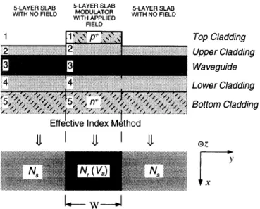
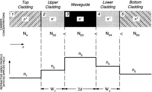
A schematic of the dielectric-loaded strip phase modulator structure chosen for this project is shown in Figure 2-13. This phase modulator device is operated as a reverse biased heterojunction. In order to reduce the free-carrier absorption loss, the center waveguide modulator region was designed as a vertical
5-LAYER SLAB 5-LAYER SLAB 5-LAYER SLAB WITH NO FIELD MODULATOR WITH NO FIELD
WITH APPLIED FIELD Top Cladding Upper Cladding Waveguide Lower Cladding Bottom Cladding
Effdctive Index M4thod
I.
I 0I
IFX
I.--
W__
Figure 2-13: Schematic of an dielectric-loaded strip waveguide phase modulator. This modulator is operated with an reverse bias voltage.
p+ regions are positioned in the outer cladding regions leaving the waveguide layer
and some portions of the cladding nominally undoped. Such a design greatly reduces the overlap between the optical mode and the highly-doped regions, and minimizes the loss due to free-carrier absorption. However, the total thickness of the intrinsic semiconductor region is limited by the voltage required to achieve >2T1 phase changes for a given modulator length. The thicker the intrinsic region, the higher the voltage required to achieve >27r phase changes.
The reverse-biased phase modulators have to be designed such that the electroabsorption is minimized for the range of desired operating voltages. To avoid electroabsorption, the bandgap (determined by the material composition) of the waveguide material is chosen to be above the energy of the operating wavelength. However, the applied electric field induces a shift in the band-edge of the material via the Franz-Keldysch effect [32] [33] which, in effect, reduces the band gap. This voltage induced change in the bandgap has to be considered when
determining the operating wavelength.
The choice of a p+-i-n+ device structure for reducing the free-carrier absorption precludes the use of free-carrier effects to achieve phase modulation. Furthermore, the concerns for reducing losses due to electroabsorption prevent the use of electrorefraction to achieve phase modulation. The phase modulators used in this project utilize the linear electrooptic effect as the dominant mechanism for
achieving phase modulation of the optical waveguide modes. The actual modulator characteristics and performance depend on the composition, dimensions, and doping of the various layers. Thus, the final device design is the result of balancing acceptable insertion loss and operating voltages to achieve a device which operates at desired wavelengths.
The fabrication of the modulator chosen for this research (see Figure 2-13) is fully compatible with the processing requirements for the dielectric-loaded strip waveguides discussed earlier. Before etching the waveguide ridge, the device regions which are designated to become modulators, are p+ doped by subjecting them to a selective Be implant, and a rapid thermal annealing process. Following the waveguide ridge etch, p-type contacts are deposited on the modulator waveguide ridges, and a common n-type contact is made by metalizing the bottom of the sample. It is to be pointed out that due to limitations in the growth of the epilayers, it is not possible to achieve a true p+-i-n+, but the actual modulator structure is a p+-n--n+ heterojunction device. However, the effort should be made to keep the n--layer as intrinsic as possible. The performance of both, modulators and the waveguides, are a function of the layer thickness, composition, and carrier concentration, as well as the dimensions of the waveguide ridge.
The waveguide modulators were analyzed by using the effective index method (EIM). However, instead of using a four-layer analysis for the structure in the x-direction, a five-layer slab guide approach was chosen to account for the index changes in the cladding layers due to different carrier concentrations. The eigenvalue equation for the modes of a five-layer slab waveguide structure is derived in Appendix A. In this analysis it is assumed that the electric field generated by the reverse biased heterojunction device is fully confined to the center (ridge) region. All possible fringing effects into the side regions were neglected. Thus, the center region was treated as a five-layer slab waveguide with the p+-layer as the top cladding. The effect of the applied voltage on the effective index of the center region can be modelled using a perturbation approach, or a more exact series solution approach [17]. This makes it possible to calculate the effective index of the center region N,(Va), as a function of the applied modulator voltage Va. Thus, by combining the effective index of the center region Nr(Va), and the unperturbed effective index of the side regions Ns, the overall propagation constant 3(Va) can be calculated using the symmetric tree-layer waveguide analysis
discussed in Section 2.1.2. The net change in the phase of the propagating mode due to an applied voltage is then given by
aO = P(V()
- P(O)
(2.64)
where P(0) is the propagation constant of the waveguide mode without applied voltage.
2.3.1 Linear Electrooptic Effect in Zinc Blende 43m Crystals
The GaAs-AlGaAs compounds used in this research are crystals of the zinc blende 43m symmetry class. This section will describe the change in optical properties of such crystals under the influence of an external electric field-electrooptic effect.
The linear electrooptic effect is the change in the index of refraction caused
by and is proportional to an applied electric field. In general, the direction
dependent index of refraction of a lossless material can be described by its impermeability and the changes thereof as follows
1nx
0
0
Axi
A
16
AK
5K = Kj+ AKij(E) = 0 1/n , O1/n + AK2 AK4 (2.65)
0 0 1/n 2 AK5 AK
4 AK3
When referring to phase modulators, K denotes the impermeability tensor of a material (not the coupling coefficient). The linear change in the coefficients AK due
to an arbitrary field E(Ex,, Ey,, Ez ,) is defined by
AK 1 AK2 AK. 3 AK 4 AK 5 AK 6 , A•(/n 2)1 A(1/n2)2 A ( /n 2 ) 3 A (1/n 2)4 A )52
A (1/n
2)6 rll r12 r 13 r21 r22 r32 r31 r32 r 33 iQr42 r34 r51 jr 35 r61 r6 2 3 E] Ej, (2.66)E
LZJ
The 6x3 matrix with elements r11 is called the electrooptic tensor. The form of the
tensor can be derived from crystal symmetry considerations, which dictate which of the 18 tensor coefficients are zero, as well as the relationship that exists between the remaining coefficients [34]. In crystals of the zinc blende 43m symmetry class there are only three nonzero elements r41=r5 2=r'36 0 (see the circled elements in Equation (2.66)). The coordinate system x', y', z', is determined by the