HAL Id: hal-01128108
https://hal.archives-ouvertes.fr/hal-01128108
Submitted on 10 Mar 2015HAL is a multi-disciplinary open access
archive for the deposit and dissemination of sci-entific research documents, whether they are pub-lished or not. The documents may come from teaching and research institutions in France or abroad, or from public or private research centers.
L’archive ouverte pluridisciplinaire HAL, est destinée au dépôt et à la diffusion de documents scientifiques de niveau recherche, publiés ou non, émanant des établissements d’enseignement et de recherche français ou étrangers, des laboratoires publics ou privés.
Functionalized nanoporous track-etched b-PVDF
membrane electrodes for lead(II) determination by
square wave anodic stripping voltammetry
Haad Bessbousse, Iris Nandhakumar, Maxime Decker, Murat Barsbay, Olivia
Cuscito, Didier Lairez, Marie-Claude Clochard, Travis L Wade
To cite this version:
Haad Bessbousse, Iris Nandhakumar, Maxime Decker, Murat Barsbay, Olivia Cuscito, et al.. Func-tionalized nanoporous track-etched b-PVDF membrane electrodes for lead(II) determination by square wave anodic stripping voltammetry. Analytical Methods, Royal Society of Chemistry, 2011, pp.1351. �10.1039/c1ay05038a�. �hal-01128108�
*Corresponding authors
Functionalized Nanoporous Track-Etched -PVDF Membrane Electrodes for Lead(II) determination by Square Wave Anodic Stripping Voltammetry
Haad Bessbousse1, Iris Nadhakumar2, Maxime Decker1, Murat Barsbay3, Olivia Cuscito1, Didier Lairez4, Marie-Claude Clochard1,*, Travis. L. Wade1,*
1
Laboratoire des Solides Irradiés, CEA-CNRS-Ecole Polytechnique, 91128 Palaiseau France 2 School of Chemistry University of Southampton University Road Southampton S017 1BJ UK 3 Hacettepe University Department of Chemistry Polymer Chemistry Division 06800 Beytepe Ankara Turkey
4Laboratoire Léon Brillouin
CEA-CNRS UMR 12, CEA-Saclay 91191 Gif-sur-Yvette, France
Abstract
Track-etched functionalized nanoporous -PVDF membrane electrodes, or functionalized membrane electrodes (FME), are thin-layer cells made from track-etched, poly(acrylic acid) (PAA) functionalized nanoporous -poly(vinylidene fluoride) (-PVDF) membranes with thin Au films sputtered on each side as electrodes. The Au film is thin enough that the pores of the membranes are not completely covered. The PAA functionalization is specifically localised in the walls of the nanoporous -PVDF membrane by radio grafting. The PAA is a cation exchange polymer that adsorbes metal ions, such as Pb2+, from aqueous solutions thus concentrating the ions into the membrane. After a calibrated time the FME is transferred to an electrochemical cell for analysis. A negative potential is applied to the Au film of the FME for a set time to reduce the adsorbed ions onto the Au film working electrode. The other metalized side of the FME functions as a counter electrode. Finally, square-wave anodic stripping voltammetry (SW-ASV) is performed on the FME to determine the metal ion concentrations in the original solution based on calibration. The calibration curve of charge versus log concentration has a Temkin isotherm form. The FME membranes are 9 m thick and have 40 nm diameter pores with a density of 1010 pores/cm2. This high pore density provides a large capacity for ion adsorption. Au ingress in the pores during sputtering forms a random array of nanoelectrodes. Like surface modified electrodes for adsorptive stripping voltammetry, the pre-concentration step for the FME is performed at open circuit. The zero current intercept of the calibration for Pb2+ is 0.13 ppb (g/L) and a detection limit of 0.050 ppb based on 3S/N from blank measurements. Voltammetry (CV) and chronoapmerometry (CA) were used to characterize the system. The apparent diffusion coefficient (D) for Pb2+ in the PAA functionalized pores was determined to be 2.44 x 10⁻⁷ cm2/s and the partition coefficient (pKM) was determined to be 3.08.
The maximum allowable levels for toxic metals in water are now set at low ppb (g/L) levels. The maximum levels of Pb2+ in potable water established the European Environmental Agency (EEA) the United States Environmental Protection Agency (EPA) and
recommendations from the World health Organisation (WHO) are 7.2, 15.0, and 10.0 ppb respectively and the goal of the United States EPA is zero. 1-3 Reliable quantification of these low concentrations is difficult time consuming and expensive. Also, the analysis equipment is not portable so the samples have to be sent a centralised lab which typically involves a 24 hour turn around time, which means that pollution events can be missed, or detected too late.
Electrochemical analysis techniques, such as anodic stripping voltammetry (ASV), are generally inexpensive, rapid and portable. The electrode of choice for measuring trace levels of toxic metal ions by ASV has been the dropping mercury electrodes (DME).4 DMEs and mercury film electrodes are very sensitive, due to their high capacity to preconcentrate ions for analysis by electro reduction, and DMEs can measure a large range of ions.5-7 The problem with mercury is that it is unacceptable for environmental applications because of its toxicity. Also, DMEs are expensive and difficult to use. Currently, there is interest in finding replacement electrodes for the DME and mercury films.8
A new industry, based on thick-film screen-printed electrodes, has evolved to exploit the growing interest in environmental sensors and to replace mercury. 9-11 Screen-printed electrodes are cheap and disposable but the quoted limits of detection (LOD) are barley able to measure the required low concentration levels.9-14 Also, these quoted LODs for screen-printed electrodes can be misleading because they are based on 3S/N background measurements made in ideal laboratory environments.
There have been very impressive results for the detection of Ag+ and As3+ by ASV using electrodes that do not contain mercury with LODs as low as 0.0005 ppb for Ag+ and 0.005 ppb for As3+. 15-19 Lead(II) LODs are somewhat higher on non mercury electrodes with the lowest Pb2+ LOD being 0.020 ppb using in situ bismuth-films on a glassy carbon electrodes modified with calixarene.20 Other good Pb 2+ LODs of ~0.1 ppb have been obtained on silver rotating disks electrodes, carbon electrodes modified with poly(pyrrole-malonic acid) and in
situ bismuth modified gold or carbon paste electrodes. 21-23 The quoted LODs for mercury free screen-printed electrodes for Pb2+, however, are about 0.4 ppb.9-11
We have developed a new type of thin-layer cell for use as electrochemical sensors for voltammetric analysis, figure 1a. The new cell is based on track-etched poly(acrylic acid) (PAA) functionalized nanoporous -poly(vinylidene fluoride) (-PVDF) membranes with porous gold electrodes on each side that function as working and counter electrodes for voltammetry, functionalized membrane electrodes (FME). The polymer film of a FME has chemically functionalized parallel nanopore channels of uniform diameter, figure 1b. The nanopore channels are formed by heavy ion irradiation and chemical etching.24 The heavy ion irradiation produces damage tracks in the form of radicals from broken carbon-carbon bonds. These radicals are very stable in -PVDF due the crystallinity of the polymer.24 The radical tracks are chemically etched to reveal nanopore channels and the channel diameters are proportional to the etching time. After the etching, however, there are still radicals within the pores. These remaining radicals can be reacted with different monomers, such as RCOOH from acrylic acid (AA) to impart chemical functionalization to the nanopore interior without blocking the pores. The functionalized nanoporous -PVDF membranes are then transformed into electrodes by the deposition of a thin gold or conductive layer onto the membrane surfaces to make an electrically conductive thin film. The metallic layer is thin enough (35 nm) that is does not completely cover the pores. Also, the gold partially ingresses the nanopores during the sputtering. 25 When the FMEs are immersed in a liquid sample they can selectively absorb certain ions, such as Pb2+, depending on their functionalization. They can then be removed from the sample, rinsed, and placed in an electrochemical cell for ASV analysis. -PVDF is a very durable material with chemical and mechanical properties similar to Teflon and is nontoxic.
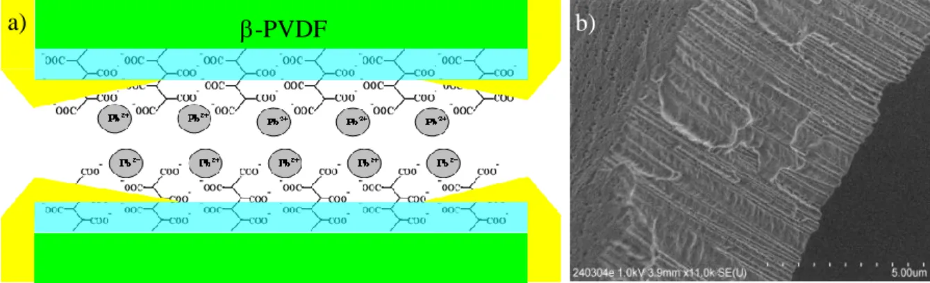
Figure 1. a) Scheme of a nanopore from a gold coated PAA functionalized radio-track etched
-PVDF membrane (FME) after absorbing Pb2+ ions from polluted water. The -PVDF membrane is shown as green and the RCOO- as blue represents the PAA gel that is radio grafted into the 40 nm diameter nanopores of the membrane. The 35 nm thick gold coating is shown as yellow. The grey balls represent the absorbed Pb2+. d) FESEM image of a track etched -PVDF membrane cross-section with pore diameter of 50 nm, membrane thickness of 10µm.
EXPERIMENTAL
Materials: -poly(vinylidene fluoride) (-PVDF) films of 9 µm thickness were provided by PiezoTech SA. Toluene, potassium hydroxide, potassium permanganate, potassium disulfite, acrylic acid (AA), Mohr’s salt ((NH4)2Fe(SO4)2 6H2O), sulphuric acid, C8H17N3 HCl (EDC),
phosphate buffer saline (PBS), tBuOK (C4H9OK 95%) were purchased from Sigma-Aldrich.
Alexa Fluor R 488 hydrazide (C21H15N4NaO10S2) was purchased from Invitrogen.
Irradiation: Prior to the swift heavy ion irradiation -PVDF films are toluene-extracted for 24 h. The irradiation was performed at the GANIL irradiation centre (Caen, France). Films were irradiated with Kr ions (10.37 Mev/amu, fluence 107 to 1010 cm−2) in a He atmosphere. The irradiated films were stored at -20°C in a N2 atmosphere until chemical etching and radio
grafting.
Chemical etching: -PVDF irradiated films were chemically etched using permanganate solution (0.25 M) in a highly alkaline medium (KOH, 10M) at 65°C for 30 min. After etching the membranes obtained were washed in potassium disulfite solution (15%) and deionized water.
Radiografting: Etched -PVDF films were immersed at room temperature into a radio grafting solution containing AA and Mohr’s salt (0.25%w/w) in a purgeable glass tube and then connected to a Schlenk line. After 15 min of N2 bubbling at room temperature, the glass
tube is sealed and put into a thermostated water bath at 60°C for 1 h. The radio grafted film is washed with water and then Sohxlet extracted in boiling water for 24 hours in order to extract free homopolymer. The membrane was dried at 50°C under vacuum overnight.
Field-Emission Scanning Electron Microscopy (FESEM): FESEM micrographs were
acquired with a Hitachi S-4800 microscope.
-PVDF membrane
Infra-red spectroscopy: FTIR spectra of PVDF were obtained with a Nicolet Magna-IR 750
spectrometer equipped with a DGTS detector. Spectra were recorded in Attenuated Total Reflexion mode (ATR) using a diamond-crystal with single reflection. Spectra were collected by cumulating 32 scans at a resolution of 2 cm−1.
Confocal Scanning Laser Microscopy (CSLM): Measurements were performed with a Leica
TCS-SP2 using a Ar laser (488 nm). Samples were observed in water with a 40× dry objective of numerical aperture 0.85
Atomic Force Microscopy (AFM): AFM images were acquired by tapping mode in air on a
Multimode AFM system equipped with a Nanoscope III controller.
Solutions: The Pb2+ solutions were diluted from 1.000g/mL AAS calibration standards (Alfa Aesar) or from PbCO3 powder 99% (VWR). The electrolyte for the voltammetry
measurements was 0.1 M sodium acetate (Sigma-Aldrich). All solutions were made with 18 Mohm deionised water (Aquadem Veolia). 100 ml polypropylene containers (VWR) were used for dilution and analysis to avoid loss of Pb2+ due to surface adsorption on glass. 26
Connections: The functionalized membrane was metalized by gold sputtering on both sides
with a K550 gold sputter (EMITECH). Gold sputtering targets were purchased from NewMet (New Metals & Chemicals LTD). The metalized sides are then connected to 0.5 mm diameter stainless steal wires with silver paste (FERRO, CDS Electronique). The connections were water proofed with hot wax and fingernail polish. Kapton tape (3M) was used to cover the surface of the electrode for some experiments.
Voltammetry: The voltammetry was performed in a three-compartment electrochemical cell
controlled by a PalmSens potentiostat (PalmSens) or a BiStat 3200 (Uniscan). A Ag/AgCl (3M KCl) reference electrode (METROHM) was used for all measurements.
RESULTS AND DISCUSSION
The synthesis of functionalized radio grafted -PVDF membranes was developed at the Laboratoire des Solides Irradies. 24, 27-32-PVDF polymer films are first bombarded by swift heavy ions, figure 2a, and the tracks formed along the ion passage are revealed under alkaline chemical treatment, figure 2b.The obtained nanoporous polymer membranes do not need to undergo subsequent e-beam irradiation to increase radicals in the polymer bulk for submicron pore diameters. After etching times less than one hour, the radical residues within the nanopore walls were sufficient for radio grafting .24 A confocal laser imaging study clearly shows that the PAA is localized inside the pores, figure 2d.
10 M etching b) a) c)
PAA grafting
Figure 2. a) 9 µm thick -PVDF films were irradiated with Kr ions (10.37 Mev/amu, fluence 107 to 1010 cm−2) under a He atmosphere. The dashed red arrows indicate the path of the Kr ions and the black/grey areas indicate the zone of irradiation damage in the film. b) The ion tracks were revealed under chemical etching. c) Fluorescein isothiocyanate labelling reveals amine groups (green), i.e. surface oxidation and Alexa Fluor R hydrazide labelling reveals carboxyl group (blue), i.e. PAA.
Indeed, when a heavy ion crosses the PVDF film, it deposits an important quantity of energy all along the latent track. This energy per mass unit (dose) is radially distributed from the ion trajectory. The energy transferred to the electrons of the polymer atoms by ion irradiation generates: defects (cross-links, chain scissions, double bonds); the creation of new active species (radicals) and gas release. The main defects in PVDF have been established by FTIR [25-27], DSC or X-ray diffraction [28]. The rapid diffusion of radicals may be related to either individual diffusion of small radical species or cooperative modes of lone electron diffusion [29]. The radical migration, initiated by the ion dose deposition, is localized in a cylinder centred around the ion trajectory with a radius roughly equal to 1µm. EPR spectra recorded under vacuum1 show the presence of various alkyl radicals (R●): end chain radicals (CF2-H2C●) or (CH2-F2C●) and middle chain radicals (CF2-HC●- CF2) or (CH2-FC●-CH2). As
soon as alkyl radicals are in contact with air, they immediately combine with the oxygen to form peroxyl radicals (ROO●) which are characterized by a loss of hyperfine structure in the EPR signal. EPR signals are consequently representative of both alkyl and peroxyl species whatever the accelerated particle.
Damage created by ion irradiation of a polymer film display a radial profile from the track core over micrometer distances. The chemical etching removes only a fraction of these defects when stopped at submicron pore opening. In most cases, the chemical etching annihilates the residual radicals leading to a radically inactive membrane. A remarkable property of -PVDF is that it favours the radical stability by trapping them inside its crystalline areas [30,31].
The radical loss of ion irradiated PVDF film at the etching temperature of 65°C was also studied. However, 60% of radicals are kept intact even after 150 min. The radical consumption by chemical etching leads to only 5% after 150 min. It demonstrates a non preponderant effect in radical decay by temperature annealing in comparison to radical consumption by etching.
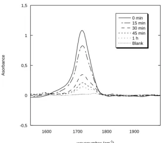
Figure 3 shows the evolution of the residual radical fraction and the radio-grafting versus etching time. The exponential profile of the radical distribution is clearly seen.
After up to one hour of track etching, the EPR signal base line is roughly horizontal. After two hours, the baseline was no longer horizontal due to the prolonged contact with potassium permanganate which incorporated oxygen radicals into the film. A baseline correction was then necessary to extract the EPR results. Actually, we can only measure the overall radical contribution with no discrimination between alkyl and peroxyl radical fractions. As plotted in Figure 3, the overall radical fraction xa(t) displays an exponential decay with a characteristic
rate of 0.055 min-1. The presence of a persistent non-decaying radical fraction of 17% was unexpected. Indeed, as the polymer is progressively removed by etching, a continuous
decrease of radicals should be observed. It results from a compensative effect between the removal of alkyl radicals by etching and the creation of peroxyl radicals by oxidation of the remaining alkyl radicals.
0 0.2 0.4 0.6 0.8 1 1.2 0 0.2 0.4 0.6 0.8 1 1.2 0 50 100 150 200 0 50 100 150 P e ro x yl r ad ic a ls fr act ion N or m al ized g ra fti ng yi el d ( Y /Y o )
Etching time (min) R (nm) -1000 -500 0 500 1000 1500 340 345 350 355 360 non-etched 120 min 180 min Magnetic field (mT)
Figure 3. Decay of peroxyl radicals fraction (●) and grafting yield (○) versus etching time. The initial grafting yield value was Y0=8 wt%. The R scale corresponds to pore radii after an
etching time t : R=0.8×t.
In the presence of vinyl monomers such as AA, a radical polymerization takes place by a radio grafting to specifically functionalize the nanopore walls with a polymer hydrogel. Figure 4 illustrates the AA grafting yield in track-etched PVDF membranes at various etching times. It shows that the radicals persist after etching and are concentrated on the pore walls of the PVDF membranes and are able to initiate a grafting in the presence of a vinyl monomer such as acrylic acid (AA) by radical polymerisation.
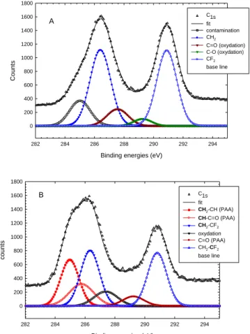
-0,5 0 0,5 1 1600 1700 1800 1900 0 min 15 min 30 min 45 min 1 h Blank A so rb a n ce wavenumber (cm-1 )
Figure 4. FTIR spectra in transmission mode in the region of carboxylic acid peak at 1710 cm
-1
for AA grafted track-etched membranes at different etching times – blank experiment corresponds to 30 min etched PVDF membrane without grafting – Irradiation and grafting conditions: 10.9 MeV/mau 58Ni25+ ions, fluence 109.cm-2, [AA]=100%, 60°C, 1 hour.
The decrease of the carboxylic acid peak at 1710 cm-1 from FTIR for increasing etching times also follows an exponential decay. It could be directly related to EPR results. Consequently, the radical distribution profile in a track drives the radical polymerisation.
One hour etching time corresponds to pores of 44 nm of radius. Above this value, the radio-grafting is no longer homogeneous and the degree of radio-grafting becomes very low (< 2wt%). As alkyl radicals are well-known to be more efficient as initiators in comparison to peroxyl radicals in radio-grafting process on solid polymers, the results lead to the conclusion that after two hours of etching, alkyl radicals are no longer present.
As the radical concentration decreases with the etching time, longer grafted PAA chains are favoured when the pore size increases but, simultaneously, the density of grafted PAA chains on the pore wall surface becomes very low. For a better coverage of pore walls, it is preferable to have shorter PAA chains and a denser grafted PAA chains layer. A good compromise was to radiograft pores with radius as small as 25 nm to have sufficient radicals for a good covering of pore walls.
In Figure 5, the XPS spectrum represents the surface composition of all atoms linked to C1S
onto track-etched PVDF membranes before and after PAA grafting. The C1S ray spectrum of
the initial track-etched -PVDF (Fig. 6A) displays, after peak deconvolution, two typical peaks of the same height and area for CH2 and CF2 of the PVDF at 286.5 eV and 291 eV
respectively. Two additional peaks at 287.8 eV and 289 eV correspond to surface oxidation peaks. The peak present at 285 eV is due the presence of non-removable PDMS contaminant present in 9 µm thick -PVDF. Even a 24h toluene extraction did not remove these alkyl contaminants coming from grease used during the initial extrusion process. Figure 6B displays the C1S ray spectrum of PAA radiografted PVDF track-etched membrane
(PVDF-g-PAA). The deconvoluted signals show not only the two peaks of PVDF but also an increase of alkyl C1S contribution as well as COOH peak. This gives evidence of PAA characteristic
allowing an estimation of the PAA coverage onto the track-etched -PVDF from peaks integrations. Only 34% of the total surface at a fluence of 107 tracks per cm-2 was covered by PAA. It confirms the heterogeneity of grafting on the PVDF-g-PAA membrane surface and it gives us supplementary proof of the specific localisation of grafted PAA inside the tracks and not on the non-irradiated part of the surface of PVDF-g-PAA membranes.
Binding energies (eV)
282 284 286 288 290 292 294 Counts 0 200 400 600 800 1000 1200 1400 1600 1800 C1s fit contamination CH2 C=O (oxydation) C-O (oxydation) CF2 base line A
Binding energies (eV)
282 284 286 288 290 292 294 counts 0 200 400 600 800 1000 1200 1400 1600 1800 C1s fit CH2-CH (PAA) CH-C=O (PAA) CH2-CF2 oxydation C=O (PAA) CH2-CF2 base line B
Figure 5. C1S ray of XPS spectrum of (A) track-etched PVDF membrane (fluence 107.cm-2)
and (B) grafted PAA track-etched PVDF membrane (PVDF-g-PAA) (fluence 107.cm-2). Etching conditions: 30 min, 65°C in KOH 10N and KMnO4 0.25N; grafting: AA aqueous
solution of 5% at T=60°C for 1h.
The PAA grafting yields used for the FMEs were usually 10 to 15%. Higher grafting yields resulted in pores that were mostly filled by PAA hydrogel so it was impossible to have open pores for ion adsorption after the gold sputtering. Lower grafting yields indicated that the grafting did not work probably due O2 contamination from insufficient N2 purging of the
grafting tube or the grafting tube was not well sealed.
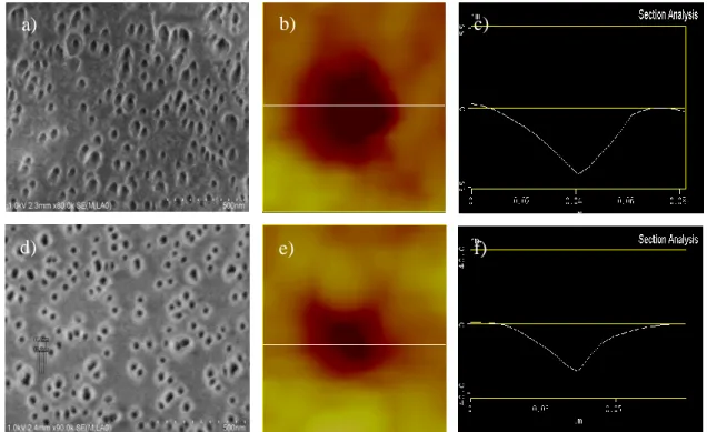
FESEM and AFM images indicate the nature of the radiografted PAA, figure 6. For the ungrafted membrane the pore diameter is about 40 nm, figures 3a-c, while the diameter of the PAA grafted membrane is about 30 nm, figures 3d-f, showing that about a 5 nm of PAA is grafted onto the walls of the nanopores. This further indicates that there are radicals within the pore walls and the PAA is intercalated into the -PVDF matrix as well as the surface of the pore walls. The lighter grey areas around the pores in the FESEM image, figure 3d, indicate a higher density material which is the PAA intercalated into the -PVDF.
Figure 6. a-c) FESEM photo, AFM image and AFM line profiles of an ungrafted -PVDF membrane irradiated with a fluence of 1x10¹⁰ ions/cm2 and 30 minutes of etching and d-f) the same membrane after PAA grafting.
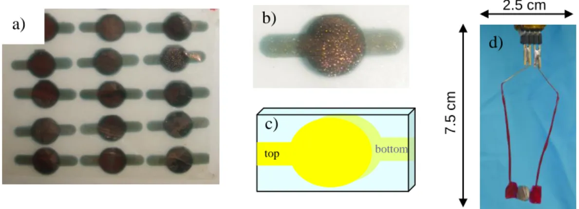
To transform the funtionalized membrane into an electrode, a thin (35 nm) Au film is sputtered through 0.4 cm diameter holes in a home made aluminum mask onto each surface, figures 7 and 8a. From the FESEM micrograph in figure 7b it is clearly seen that the pores of the film remain open after sputtering, however, Au does ingress the membrane pores.25 The Au, which protrudes into the membrane’s pores, forms 30 nm diameter, 100 nm long nanoelectrodes. The result is a membrane of with random array of 1010 parallel nanoelectrodes/cm2 separated from the counter electrode by 9 m long 30 nm diameter pores. After sputtering the Au film through a mask, figure 8a, a 1.5 x 0.6 cm square of membrane is cut out, figures 8b and c, and connected to stainless steel wires with silver paste. The contacts are first protected with hot wax and then fingernail polish, figure 8d.
a) b) c) d) e) f) b) P V DF f il m a) 35 nm Au film
Figure 7. a) Scheme of a 9 m thick functionalized -PVDF membrane (green) with a 35 nm sputtered gold film (yellow) on each side. b) FESEM photo of a 9 m thick functionalized -PVDF membrane with a 35 nm Au film sputtered on the surface.
Figure 8. a) Photo of a 35 nm thick gold layer sputtered on each side of the functionalized -PVDF membrane through a mask. b) and c) Photo and scheme of a metalized membrane cut out from the large surface from photo a). d) Photo of a membrane attached to wire leads with silver paste and protected with wax and fingernail polish for connection to a potentiostat.
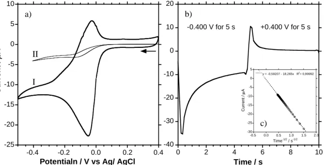
Before a FME is used, a cyclic voltammogram (CV) is performed in a blank solution (0.1 M sodium acetate pH 4.5), figure 9a. In spite of the fact that the gold layer on the PVDF membrane is only 35 nm thick the CV shows the typical profile of a polycrystalline Au electrode.33 The CV was performed on the membrane starting at 0.0 V and ramped at a scan rate of 20 mV/second to +1.2 V where the scan was reversed until the scan was stopped at +0.2 V. The other side of the FME was the counter electrode. This configuration of the working and the counter electrodes is essentially that of a thin-layer cell.34-36
Figure 9. a) 0.4 cm diameter Au CV in 0.1 M CH3COONa, pH ~4.5 (scan rate = 20 mV/s).
The arrows indicate the sense of the scan.
top bottom 2.5 cm 7.5 c m a) b) c) d) -15 -10 -5 0 5 10 15 20 0 0.2 0.4 0.6 0.8 1.0 1.2 C u rr e n t / A Potential / V vs Ag/AgCl a) 0.3 0.2 0.1 0.0 -0.1 -0.2 1.2 1.0 0.8 0.0 0.2 0.4 0.6 b)
formed at potentials more positive than 0.850 V during the positive scan. 33 Integration of this reduction peak between 0.400 and 0.800 V gives a charge of 75C. The charge for the oxidation of a monolayer of gold (111) is 482 C/cm2.33 This gives an area of 0.1556 cm2, however, the visual area of the FME is 0.126 cm2, 0.40 cm diameter, so the roughness factor (RF) of the electrode is 1.24. This high RF is likely due to the gold ingress in pores of the membrane during the sputtering, figures 1a and 7a.25 Figure 9b shows the same experiment as figure 9a except the surface of the working was covered with Kapton tape inorder to limit the measured current to the gold which ingresses in the pores of the membrane. This gives a surface area of 0.00229 cm2, based on the same calculation as figure 9a. If we consider that the Au inside of the pores is 30 nm diameter disks then a geometric calculation of the surface gives a surface area of 0.00879 cm2 so what we have measured by the CV in figure 9b is about 25% of the disk model, however, is probably in the form of Au tubes with an outside diameter of 30 nm with an unknown internal diameter and unknown length. The obvious thing to do would be to dissolve the membrane and observe the membranes side of the gold surface as was done by Vaidyanathan et al. with polycarbonate membranes with 200 nm diameter pores.25-PVDF is, however, difficult to dissolve and 30 nm structures are still a bit of a challenge to characterize so this is an on going study.
A CV of the FME in the same solution as figure 9a with 0.025 mM Pb2+ added at a scan rate of 100 mV/s (curve I) shows the electrochemical behaviour for the reduction and oxidation of the Pb2+, figure 9b. The Pb2+ reduction current peak occurs at -0.054 V and the oxidation peak occurs at -0.033 V. The reduction peak current is ~14 A and the oxidation peak current is ~9 A. Even though the peak separation is only 0.021 V the difference in currents indicates the irreversibility of the Pb2+ on Au. This could be the result of alloy formation or oxidation of the deposited Pb by oxygen present in solution since no purging of the solution was performed. At a scan rate of 2 mV/s (curve II) the CV is sigmoid indicating that at long times the diffusion steady-state.
Figure 10a) CVs of a FME in a 0.025 mM Pb2+ solution with 0.1 M CH3COONa, pH ~4.5
(curve I scan rate = 100 mV/s and for curve II scan rate = 2 mV/s). b) Chronoamperometric plot of a FME in a 0.0966 mM Pb2+ solution with 0.1 M CH3COONa, pH ~4.5. c) Current
versus time-1/2 plot of the reduction part of the chronoamperometric plot. -25 -20 -15 -10 -5 0 5 10 Curr e n t / A
Potentialn / V vs Ag/ AgCl
-0.4 -0.2 0.0 0.2 0.4 a) -40 -30 -20 -10 0 10 20 0 2 4 6 8 10 Time / s -0.400 V for 5 s +0.400 V for 5 s -30 -25 -20 -15 -10 -5 0 5 C u rr e n t / A Time-1/2 / s-1/2 -0.5 0.0 0.5 1.0 1.5 2.0 y = -0,59207 - 18,265x R2 = 0,99992 b) c) I II
Chronoamperometry experiments were performed based on the potential window seen for the CVs in figure 10a, figure 10b. The potential was switched form +0.400 V to -0.400 V and held for 5 seconds then switched back to +0.400 V and held for 5 seconds in order to measure the diffusion limited current (Idiff), the solution concentration was 0.100 mM Pb2+. The ratio
of the oxidation current to the reduction current (iO/iR) at a given time after the potential step
ranges from -0.124 to -0.030 which is much lower that predicted for a simple reversible reaction of -0.293. 37 A plot of the current for the reduction step versus 1/t-1/2 yields a strait line with a good fit for the linear regression, figure 10c.
The diffusion limiting current at a disk microelectrode (in terms of the disk radius) after a potential step can be described by equation 1. 38-40
Idiff = 1/2 n F D1/2Co r2 / t1/2 + 4nF DCo r (1)
The term n is equivalence/mole for the reduction (n = -2 for Pb2+, equation 5), F is the Faraday constant (96485 Coulombs/equivalent), D is the apparent diffusion coefficient (cm2/s), C is the concentration of Pb2+ (moles/L) r is the electrode radius (cm) and t time (s). The first term on the right is the Cottrell equation for linear diffusion and the second term on the right describes steady-state diffusion at a disk microelectrode. At short times linear diffusion dominates the current and at long times steady-state diffusion dominates current. A very convenient graphical analysis of this behaviour at a disk microelectrodes was detailed by Hepel et al.40 The plot of I versus t-1/2 (figure 7c) has a slope equal to Is 1/2 r / D1/2 and an
intercept of Is / 4 where Is equals the steady-state current. The intercept of the line (b) and
the slope (k) can be determined from equations 2 and 3. 39, 40
D = (br/k)2 / (2)
Co = k2 /4nFbr3 (3)
The slope and the intercept can be taken directly from the linear regression formula in figure 10c. The radius, r, was found from the area determined from figure 9b by dividing by and taking the square root, r = (A/)1/2. This was used since the total current is the sum of all the individual nanoelectrodes. 41 The values determined from the plot in figure 10c for D is 2.44 x 10⁻⁷cm2/s for Pb2+ in the nanopores and a Pb2+ concentration, Co,of 116.6 mM.
Geary et al. studied the diffusion of Pb2+ colloidal hydrogel with and without a binding agent to complex the Pb2+. They determined a diffusion coefficient for Pb2+ in bulk solution of 9.45 x 10⁻⁶cm2/s. In porous media with no Pb2+ pore interactions (i.e. no binding agent) the diffusion coefficient was 6.72 x 10⁻⁶ cm2/s and with Pb2+/pore interactions the value ranged from 12.60 to 2.84 x 10⁻⁷cm2/s, depending on the Pb2+ concentration. 42 Our value determined for PAA grafted -PVDF nanopores is lower than those found by Geary et al. but PAA is also a stronger binding agent than that used in the colloidal hydrogel, benzo-18-crown-6, pKM =
2.75. The diffusion of Cu2+ in 36 nm diameter nanoporous polycarbonate membranes was determined to be 0.7 x 10⁻⁶cm2/s as opposed to the bulk value of 3.0 x 10⁻⁶cm2/s. 43
During the immersion of a FME in a sample containing heavy metal ions, the membrane absorbs some of the metal cations by the PAA grafted in the nanopores of the -PVDF membrane, equation 4. The pKM of Pb2+ in bulk PAA is 4.0 at pH < 4.0, determined by
potentiometric titrations and ion-selective electrodes.44 The value we determined from figure 10c and equation 3 is 3.08.
For the electrochemical analysis the FME is connected to a potentiostat and placed at a negative potential. The negative potential reduces the absorbed metals ions that are very close to the working electrode, from the poly (acrylic acid) in the pores to their metallic state at the Au surface, equation 5.
R-COO-Mn+ + ne-
--> M(Au)
(5)After the reduction, square wave anodic stripping voltammetry (SW-ASV) analysis is performed in order to oxidize the metal from the working electrode surface and measure the resulting current, equation 6.
M(Au)
--> M
n+ + ne- (6)The parameters for the SW-ASV analysis were a frequency of 25 Hz, step amplitude of 25 mV and a potential increment of 4 mV. The optimisation of the deposition potential, time and immersion time follows: The deposition potential was determined by immersing a FME in 50 ml of stirred 3 g/L Pb2+ sample for 10 minutes followed by SW-ASV. The charge increases with decreasing deposition potential, figure 11a. There is, however, a local minimum at – 0.9 V. This is likely due to the hydrogen gas bubbles from proton reduction at the FME that could impair Pb2+ deposition, equation 7.
2H+ + 2e-
--> H
2 (g) (7)Also, for potentials more negative than -0.8 V there was a problem with the gold electrode adhesion due to the formation of hydrogen gas bubbles. Therefore, a deposition potential of -0.8 V was used for further studies. The absorption time was determined by immersing a FMS in 50 ml of a 3 g/l Pb2+ sample for different times followed by deposition at – 0.8 V, figure 11b. After 30 minutes equilibrium is established. Figure 11c shows the charge versus the deposition time. After 100 seconds a plateau is reached so a minimum deposition time of 100 seconds is used for further studies.
a) b) -1.3 -1.2 -1.1 -1 -0.9 -0.8 -0.7 -0.6 Charge / C Potential / V vs Ag/AgCl 2.0 1.8 1.6 1.4 1.2 1.0 0.8 2 3 4 5 6 7 8 9 10 0 20 40 60 80 100 time / minutes 2 4 6 8 10 12 0 100 200 300 400 500 600 700 time / s c)
Figure 11. a) A plot of oxidation charge from SW-ASV scans of FMEs that were immersed in
50 ml of stirred 3 g/L Pb2+ samples for10 minutes with different deposition potentials. b) A plot of the charge versus immersion time in 50 ml of stirred 3 g/l Pb2+ samples using a deposition potential of -0.8 V. c) A plot of deposition time versus charge for a membrane that been immersed in 50 ml of stirred 3 g/L Pb2+ samples for 30 minutes with a deposition potential of -0.8 V.
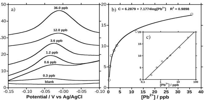
Figure 12 is a plot of superimposed SW-ASV current peaks for different concentrations of Pb2+ along with a blank scan. Each curve was obtained using a different FME. At concentrations higher than 3 to 4 g/L current/voltage curves do not increase much in height but become very broad. For this reason the calibration curve was plotted with the charge and not peak current.
Figure 12. SW-ASV analysis plots of FMEs after immersion in 50 ml of stirred Pb2+ ion solutions for 30 minutes using different concentrations. The curve from a blank analysis is also plotted. b) A calibration curve for Pb2+ ions determined from figure 8a. b) A charge vs. log concentration curve.
Figure 12b is a curve of the charges found from figure 12a versus the concentrations of the solutions measured. Different isotherms were used to fit the curve in figure 9b and a Temkin isotherm gave the best fit with a R2 of 0.98979. 4 The Temkin isotherm indicates that there is a decrease in the heat of adsorptions with increasing coverage within the pores. 45 The intercept of the charge versus log [Pb2+] plot has a [Pb2+] value of 0.13 ppb. The 3S/N, standard deviation (), of eight blank scans was 0.05 ppb.
The coefficients of variation for repeated measurements of 1.0 ppb and 12.0 ppb were 40% and 22% respectively. These coefficients of variation could reflect the variation of the PAA grafting yields which were 10-15% or more likely the reproducibility of the etching. If the temperature of the etching bath is a few degrees too low or the etching time is not sufficient some areas of the membrane have pores that are not open the entire thickness of the membrane.
A SW-ASV measurement of tap water showed no indication of Pb2+. When the same tap water sample was spiked with 3 ppb of Pb2+ the charge recovered was 88.5% of the charge corresponding to 3 ppb from the calibration curve in figures 8b and c, however, this charge only corresponds to a concentration of 1.2 ppb. This could be due to the logarithmic nature of
0 10 20 30 40 50 blank 0.3 ppb 1.2 ppb 3.6 ppb 12.0 ppb 0.6 ppb 36.0 ppb Potential / V vs Ag/AgCl Curr e n t / A -0.15 -0.10 -0.05 -0.00 -0.05 -0.100 5 10 15 20 0 5 10 15 20 25 30 35 40 [Pb2+] / ppb C = 6.2879 + 7.1774log[Pb2+] R2 = 0.9898 0 5 10 15 20 0,1 1 10 100 [Pb2+] / ppb a) b) c)
Or the discrepancy could be due to a masking of Pb2+ by something in the tap water or perhaps complex formation by an anion such as Cl- or F-.
CONCLUSIONS
The partition coefficient, pKM, is lower for the PAA functionalized -PVDF nanopores than
bulk PAA by a factor of 10. This could also be a result of the uncontrolled polymerisation of the PAA. A dense hydrogel of PAA in the nanopores might not adsorb as well as more open bulk PAA or it might be difficult for the electrodeposition to efficiently extract the adsorbed Pb2+ from the PAA in the nanopore walls. The methods used to determine the pKM for the bulk PAA were very different were a measure of the Pb2+ uptake from solution and was not a measure of the Pb2+ in the PAA. The measured diffusion coefficient is constant with diffusion coefficients for Pb2+ and Cu2+ in nanoporous media if not lower reflecting the interaction of the Pb2+ with the grafted PAA.
The FME is very sensitive to sub-ppb concentrations of Pb2+. The membrane preparation is done in bulk and is very inexpensive in materials. The most expensive step is the gold metallisation. We are in the process of functionalizing the PVDF membranes with polymers other than PAA to evaluate different ion adsorption efficiencies and selectivities. Because of their versatility, the FME can be thought of as a template for electroactive polymers as ion sensors.
Problems of reproducibility are likely caused by some variations in membrane etching and in the reproducibility of the grafting yields. The Temkin isotherm indicates that the energy of adsorption of Pb2+ is inhomogeneous in the PAA functionalized membrane so there is a need to develop techniques to improve the uniformity of the PAA polymerisation. We are currently working on improving the reproducibility of the grafting yield by studying Reverse Addition Fragmentation Transfer Polymerization inside tracks. The kinetics of the adsorption isotherm needs also to be addressed in order to understand and better optimize the adsorption.
The adsorption is done at open circuit and the SW-ASV analysis is very fast, less than 3 minutes. The ability to preconcentrate the ions at open circuit means that many samples can be collected in parallel and stored for later analysis.
REFERENCES
1. DIRECTIVE 2008/105/EC. In European Environment Agency: 2008; p 10.
2. Guidlines for Drinking-water Quality. In World Health Organisation: 2008; Vol. 1, p 392.
3. National Primary Drinking Water Regulations. In United States Environmental Protection Agency: May 2009; p 3.
4. Brett, C. M. A.; Brett, A. M. O., Electrochemistry Principles, Methods, and
Applications. 1st ed.; Oxford University Press: Oxford, 2005.
5. Bahrami, S.; Abbasi, S.; Ghorbani, Y. A.; Miran-Beigi, A. A., High sensitive determination of trace amount of cobalt by catalytic adsorptive stripping voltammetry.
Russian Journal Of Electrochemistry 2009, 45, (2), 208-214.
6. Fischer, E.; van den Berg, C. M. G., Anodic stripping voltammetry of lead and
cadmium using a mercury film electrode and thiocyanate. Analytica Chimica Acta 1999, 385, (1-3), 273-280.
7. Jakubowska, M.; Zembrzuski, W.; Lukaszewski, Z., Thallium determination at the single picomole per liter level by flow-injection differential-pulse anodic stripping
voltammetry. Electroanalysis 2008, 20, (10), 1073-1077.
8. Hutton, E. A.; Hocevar, S. B.; Ogorevc, M., Ex situ preparation of bismuth film microelectrode for use in electrochemical stripping microanalysis. Analytica Chimica Acta
2005, 537, (1-2), 285-292.
9. Laschi, S.; Palchetti, I.; Mascini, M., Gold-based screen-printed sensor for detection of trace lead. Sensors And Actuators B-Chemical 2006, 114, (1), 460-465.
10. Renedo, O. D.; Alonso-Lomillo, M. A.; Martinez, M. J. A., Recent developments in the field of screen-printed electrodes and their related applications. Talanta 2007, 73, (2), 202-219.
11. Rico, M. A. G.; Olivares-Marin, M.; Gil, E. P., Modification of carbon screen-printed electrodes by adsorption of chemically synthesized Bi nanoparticles for the voltammetric stripping detection of Zn(II), Cd(II) and Pb(II). Talanta 2009, 80, (2), 631-635.
12. Khaled, E.; Hassan, H. N. A.; Habib, I. H. I.; Metelka, R., Chitosan Modified Screen-Printed Carbon Electrode for Sensitive Analysis of Heavy Metals. International Journal Of
Electrochemical Science 5, (2), 158-167.
13. Renedo, O. D.; Martinez, M. J. A., Anodic stripping voltammetry of antimony using gold nanoparticle-modified carbon screen-printed electrodes. Analytica Chimica Acta 2007, 589, (2), 255-260.
14. Yantasee, W.; Deibler, L. A.; Fryxell, G. E.; Timchalk, C.; Lin, Y. H., Screen-printed electrodes modified with functionalized mesoporous silica for voltammetric analysis of toxic metal ions. Electrochemistry Communications 2005, 7, (11), 1170-1176.
15. Javanbakht, M.; Divsar, F.; Badiei, A.; Fatollahi, F.; Khaniani, Y.; Ganjali, M. R.; Norouzi, P.; Chaloosi, M.; Ziarani, G. M., Determination of picomolar silver concentrations by differential pulse anodic stripping voltammetry at a carbon paste electrode modified with phenylthiourea-functionalized high ordered nanoporous silica gel. Electrochimica Acta 2009, 54, (23), 5381-5386.
16. Feeney, R.; Kounaves, S. P., On-site analysis of arsenic in groundwater using a microfabricated gold ultramicroelectrode array. Analytical Chemistry 2000, 72, (10), 2222-2228.
17. Song, Y.; Swain, G. M., Development of a method for total inorganic arsenic analysis using anodic stripping voltammetry and a Au-coated, diamond thin-film electrode. Analytical
Chemistry 2007, 79, (6), 2412-2420.
18. Jena, B. K.; Raj, C. R., Gold nanoelectrode ensembles for the simultaneous
electrochemical detection of ultratrace arsenic, mercury, and copper. Analytical Chemistry
2008, 80, (13), 4836-4844.
19. Dai, X.; Nekrassova, O.; Hyde, M. E.; Compton, R. G., Anodic stripping voltammetry of arsenic(III) using gold nanoparticle-modified electrodes. Analytical Chemistry 2004, 76, (19), 5924-5929.
20. Torma, F.; Gruen, A.; Bitter, I.; Toth, K., Calixarene/Nafion-Modified Bismuth-Film Electrodes for Adsorptive Stripping Voltammetric Determination of Lead. Electroanalysis
2009, 21, (17-18), 1961-1969.
21. Brand, M.; Eshkenazi, I.; KirovaEisner, E., The silver electrode in square-wave anodic stripping voltammetry. Determination of Pb2+ without removal of oxygen. Analytical
Chemistry 1997, 69, (22), 4660-4664.
22. Heitzmann, M.; Basaez, L.; Brovelli, F.; Bucher, C.; Limosin, D.; Pereira, E.; Rivas, B. L.; Royal, G.; Saint-Aman, E.; Moutet, J. C., Voltammetric sensing of trace metals at a
poly(pyrrole-malonic acid) film modified carbon electrode. Electroanalysis 2005, 17, (21), 1970-1976.
Bi(III) concentration on the stripping voltammetric response of in situ bismuth-coated carbon paste and gold electrodes. Electrochimica Acta 2006, 52, (2), 481-490.
24. Cuscito, O.; Clochard, M. C.; Esnouf, S.; Betz, N.; Lairez, D., Nanoporous beta-PVDF membranes with selectively functionalized pores. Nuclear Instruments & Methods In Physics
Research Section B-Beam Interactions With Materials And Atoms 2007, 265, (1), 309-313.
[25] N. Betz, A. Le Moël, E. Balanzat, J.-M. Ramillon, J. Lamotte, J.-P. Gallas, G. Jaskierowicz, Journal of Polymer Science: Part B, Polymer Physics 32 (1994) 1493-1502.
[26] E. Balanzat, S. Bouffard, A. Le Moël, N. Betz, Nuclear Instruments and Methods in Physic Research B 91 (1994) 140-145.
[27] S. Bouffard, N. Betz, E. Balanzat, Nuclear Instruments and Methods in Physic Research B 105 (1995) 46-54.
[28] V. Chailley, E. Balanzat, E. Dooryhee, Nuclear Instruments and Methods in Physic Research B 105 (1995) 110-114.
[29] H. Alem, A.-S. Duwez, P. Lussis, P. Lipnik, A.M. Jonas, S. Demoustier-Champagne, Journal of Membrane Science 308 (2008) 75-86.
[30] C. Aymes-Chodur, S. Esnouf, A. Le Moël, Journal of Polymer Science: Part B: Polymer Physics 39 (2001) 1437-1448.
[31] C. Aymes-Chodur, N. Betz, M.-C. Porte-Durrieu, C. Baquey, A. Le Moël, Nuclear Instruments adn Methods in Physic Research B 151 (1999) 377-385.
25. Vaidyanathan, R.; Stickney, J. L.; Cox, S. M.; Compton, S. P.; Happek, U., Formation of In2Se3 thin films and nanostructures using electrochemical atomic layer epitaxy. Journal
Of Electroanalytical Chemistry 2003, 559, 55-61.
26. Pinheiro, J. P.; Bosker, W., Polystyrene film-coated glassware: a new means of reducing metal losses in trace metal speciation. Analytical and Bioanalytical Chemistry 2004, 380, (7-8), 964-968.
27. Betz, N.; Moel, A. L.; Pireaux, J.-J., Ionizing radiation & polymers. Nucl. Inst. Meth.
B 2005, 236, VII-VIII.
28. Clochard, M. C.; Begue, J.; Lafon, A.; Caldemaison, D.; Bittencourt, C.; Pireaux, J. J.; Betz, N., Tailoring bulk and surface grafting of poly(acrylic acid) in electron-irradiated PVDF.
Polymer 2004, 45, (26), 8683-8694.
29. Clochard, M. C.; Betz, N.; Goncalves, M.; Bittencourt, C.; Pireaux, J. J.; Gionnet, K.; Deleris, G.; Le Moel, A., Peptide immobilization onto radiation grafted PVDF-g-poly(acrylic acid) films. Nuclear Instruments & Methods In Physics Research Section B-Beam
Interactions With Materials And Atoms 2005, 236, 208-215.
30. Clochard, M. C.; Wade, T. L.; Wegrowe, J. E.; Balanzat, E., Influence of asymmetric etching on ion track shapes in polycarbonate. Nuclear Instruments & Methods In Physics
Research Section B-Beam Interactions With Materials And Atoms 2007, 265, (1), 325-329.
31. Grasselli, M.; Betz, N., Electron-beam induced RAFT-graft polymerization of poly(acrylic acid) onto PVDF. Polymer 2005, 45, (26), 8683-8694.
32. Mazzei, R.; Bermudez, G. G.; Betz, N.; Cabanillas, E., Swift heavy ion induced graft polymerization in track etched membranes' submicroscopic pores. Nucl. Inst. Meth. B 2004, 223, (4), 575-584.
33. Hoogvliet, J. C.; Dijksma, M.; Kamp, B.; van Bennekom, W. P., Electrochemical pretreatment of polycrystalline gold electrodes to produce a reproducible surface roughness for self assembly: A study in phosphate buffer pH 7.4. Analytical Chemistry 2000, 72, (9), 2016-2021.
34. Hubbard, A. T.; Anson, F. C., Linear Potential Sweep Voltammetry in Thin Layers of Solution. Analytical Chemistry 1966, 38, (1), 58-&.
35. Hubbard, A. T.; Anson, F. C., Determination of Adsorbed Cobalt and Iron Ethylenedinitrilotetraacetate Complexes on Platinum Electrodes by Thin Layer Electrochemistry. Analytical Chemistry 1966, 38, (11), 1601-&.
36. Hubbard, A. T.; Anson, F. C., New Electrodes for Chronopotentiometry in Thin Layers of Solution. Analytical Chemistry 1964, 36, (4), 723-&.
37. Rieger, P. H., Electrochemistry. Prentice-Hall, Inc.: Englewood Cliffs, NJ, 1987; p 508.
38. Longmire, M. L.; Watanabe, M.; Zhang, H.; Wooster, T. T.; Murray, R. W.,
Voltammetric Measurement of Ultraslow Diffusion Rates in Polymeric Media with Microdisk Electrodes. Analytical Chemistry 1990, 62, (7), 747-752.
39. Zhou, H. F.; Che, G. L.; Dong, S. J., Study on diffusion of electroactive species in polyelectrolyte polyethylene glycol lithium perchlorate by chronoamperometry at a microdisk electrode. Electroanalysis 1997, 9, (1), 40-44.
40. Hepel, T.; Osteryoung, J., Chronoamperometric Transients at the Stationary Disk Microelectrode. Journal of Physical Chemistry 1982, 86, (8), 1406-1411.
41. Baker, W. S.; Crooks, R. M., Independent geometrical and electrochemical
characterization of arrays of nanometer-scale electrodes. Journal of Physical Chemistry B
1998, 102, (49), 10041-10046.
42. Geary, C. D.; Zudans, I.; Goponenko, A. V.; Asher, S. A.; Weber, S. G., Electrochemical investigation of Pb2+ binding and transport through a polymerized
crystalline colloidal array hydrogel containing benzo-18-crown-6. Analytical Chemistry 2005, 77, (1), 185-192.
43. Schonenberger, C.; vanderZande, B. M. I.; Fokkink, L. G. J.; Henny, M.; Schmid, C.; Kruger, M.; Bachtold, A.; Huber, R.; Birk, H.; Staufer, U., Template synthesis of nanowires in porous polycarbonate membranes: Electrochemistry and morphology. Journal of Physical
Chemistry B 1997, 101, (28), 5497-5505.
44. Miyajima, T.; Mori, M.; Ishiguro, S., Analysis of complexation equilibria of
polyacrylic acid by a Donnan-based concept. Journal of Colloid and Interface Science 1997, 187, (1), 259-266.
45. Bond, C. G., Catalysis by Metals. 1 ed.; Academic Press Inc.: London, 1962; Vol. 1, p 519.