HAL Id: hal-00819148
https://hal.archives-ouvertes.fr/hal-00819148
Submitted on 30 Apr 2013HAL is a multi-disciplinary open access archive for the deposit and dissemination of sci-entific research documents, whether they are pub-lished or not. The documents may come from teaching and research institutions in France or
L’archive ouverte pluridisciplinaire HAL, est destinée au dépôt et à la diffusion de documents scientifiques de niveau recherche, publiés ou non, émanant des établissements d’enseignement et de recherche français ou étrangers, des laboratoires
Electric-field control of domain wall nucleation and
pinning in a metallic ferromagnet
Anne Bernand-Mantel, Liza Herrera-Diez, Laurent Ranno, Stefania Pizzini,
Jan Vogel, Dominique Givord, Stéphane Auffret, Olivier Boulle, Ioan Mihai
Miron, Gilles Gaudin
To cite this version:
Anne Bernand-Mantel, Liza Herrera-Diez, Laurent Ranno, Stefania Pizzini, Jan Vogel, et al.. Electric-field control of domain wall nucleation and pinning in a metallic ferromagnet. Applied Physics Letters, American Institute of Physics, 2013, 102 (12), pp.122406. �10.1063/1.4798506�. �hal-00819148�
Electric-field control of domain wall nucleation and
pinning in a metallic ferromagnet
A. Bernand-Mantel,1,a) L. Herrera-Diez, 1 L. Ranno, 1 S. Pizzini, 1 J. Vogel, 1 D. Givord, 1 S. Auffret, 2 O. Boulle, 2 I. M. Miron2 and G. Gaudin2
1
Institut Néel, CNRS and Université Joseph Fourier, BP 166, F-38042 Grenoble Cedex 9, France
2
SPINTEC, UMR-8191, CEA/CNRS/UJF/GINP, INAC, F-38054 Grenoble, France
a)Author to whom correspondence should be addressed. Electronic addresse: anne.bernand-mantel@grenoble.cnrs.fr
The electric (E) field control of magnetic properties opens the prospects of an alternative to magnetic field or electric current activation to control magnetization. Multilayers with perpendicular magnetic anisotropy (PMA) have proven to be particularly sensitive to the influence of an E-field due to the interfacial origin of their anisotropy. In these systems, E-field effects have been recently applied to assist magnetization switching and control domain wall (DW) velocity. Here we report on two new applications of the E-field in a similar material : controlling DW nucleation and stopping DW propagation at the edge of the electrode.
The possibility of controlling magnetic properties with an E-field via magneto-electric (ME) effects was initially envisaged in multiferroïcs1 or magnetic semiconductors2. As the majority of these materials loses their ferromagnetic properties at room temperature the recent discovery of
an important ME effect at room temperature in conventional ferromagnetic metals3-8 has attracted much attention. Despite the limited penetration depth of an E-field in metals, the charge induced at the metal/dielectric interface on the topmost atomic layers is sufficient to modify the surface magnetic anisotropy energy (MAE) by a non negligible amount in ultrathin ferromagnetic layers as suggested by electronic structure calculations9-11. This has a particular impact in systems where the different anisotropy contributions almost cancel each other out, resulting in a large relative variation of the total effective MAE when the surface contribution is modified with the voltage12-26. We have studied here a Pt/Co/AlOx sample where the surface MAE could be varied in two ways : charging the metal/dielectric interface and modifying its oxidation. We demonstrate that charging and oxidizing the interface affect the magnetic properties in some equivalent manner in this system. The E-field effect is characterized by monitoring the magnetization reversal for different MAE values. For weak MAE, we observe a nucleation-dominated reversal and we demonstrate that the thermally activated DW nucleation can be electrically controlled via the modulation of the involved energy barrier. For higher MAE we observe a strong E-field variation of the thermally activated DW creep motion, as reported in previous works22-24. In addition to this E-field control of DW velocity below the electrode we demonstrate the reversible pinning of DW at the edge of the electrode. The measurements reported here are carried out using magneto-optical Kerr microscopy. The E-field is applied locally via transparent electrodes deposited on the un-patterned dielectric/metalic bilayer, thus allowing direct comparison of the magnetic properties with and without the E-field within the same image. The metallic ferromagnetic multilayer consists of a Si/Pt(3 nm)/Co(0.6 nm)/Al(wedge ∼1.5 nm) stack prepared by sputtering. The Al wedge is oxidized in a O2 plasma,
thickness along the wedge results in a progressive variation of the Co/AlOX interface oxidation.
This oxidation has a direct impact on the magnetic anisotropy of the Co layer : for an optimum oxidation of the Co/AlOx interface the ferromagnetic layer possesses an out of plane anisotropy27. The alumina layer is subsequently covered by an Atomic Layer Deposition (ALD) grown Al2O3(∼7nm)/HfO2 (∼37nm) dielectric bilayer. Transparent top gate electrodes of 50 x
700 µm wide indium tin oxide (ITO) are deposited on top by sputtering and patterned by UV lithography. A schematic representation of the device is showed in Figure 1.
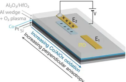
Fig. 1
:
Schematic representation of the magnetic multilayers and the device structure. Thedirection of increasing perpendicular anisotropy and increasing Co/AlOx oxidation are indicated. The two electrodes under which the E-field effect have been characterized in the low (E1) and
high (E2) anisotropy regions are represented.
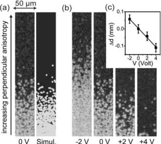
To study the E-field influence on DW nucleation we have selected a low anisotropy (higher Co/AlOX oxidation) region compared to the high anisotropy (optimum oxidation) region.
In this region a high nucleation density was observed at the time, magnetic field and length scales of our experiment. A Kerr image taken below the ITO electrode E1 200 ms after applying
Fig. 2: (a) (left) and (b) Kerr images recorded through the ITO electrode E2 200 ms after a 1 mT
constant magnetic field is applied and for different applied voltages. (a) (right) Simulation of the nucleation. (c) Displacement of the 50% reversed zone as a function of the applied voltage. Regions where the magnetization is unreversed (reversed) appear in dark grey (light grey). The nucleation density is increasing (indicating a decrease in MAE) in the direction where the Co/AlOx interface is getting more oxidized. If we refer to previous works on this system27, this confirms that the Co/AlOx interface is in the over-oxidized state in our sample. The fast variation of nucleation density suggests that the nucleation rate follows some exponential law as expected for a thermally activated nucleation process above an energy barrier. To confirm this we have calculated the nucleation probability within the Néel-Brown model (see Appendix A ). The results are presented in Figure 2.a (right). The calculation provides a qualitative description of the experimental data for a linear variation of the energy barrier height along the wedge ∆EN/∆x=0.22 meV/µm and an energy barrier height EN =500 meV (at the bottom on the image in Figure 2(a)). The influence of the E-field on the nucleation is checked by comparing Kerr images taken 200 ms after applying a 1 mT magnetic field for various V (Figure 2(b)). The region where 50% of the magnetization is reversed is linearly shifted by the E-field with a position/voltage equivalence of ∆x/∆V=30 µm/V. This shift toward lower MAE regions for
positive voltage is consistent with the MAE increase upon electron density increase already observed in previous works22,24. In addition to this, we demonstrate here an equivalence between a reduction of the electron density and an oxidation increase, in the case of an over oxidized Co/AlOx interface and we show that this E-field induced MAE variation can cause an exponential variation of the nucleation rate.
Fig. 3: (a) and (e) Kerr images of the magnetization reversal below the ITO electrode (centre) recorded a, 12, 16 and 22 s after a constant 2.4 mT magnetic field is applied and (e) for various V. The edges of the electrode are visible as two black vertical lines. (b) and (c) The black squares represent the experimental DW velocites measured (c) outside the ITO electrode at different positions on the wedge (b) below the ITO electrode around position x1 for different applied V.
where α1,2 correspond to the coefficient found for respectively (b) and (c). The ratio α2/α1 gives
the position/voltage equivalence ∆x/∆V=80 µm/V. x1 and x2 positions are indicated in (a). (c)
DW velocities measured. (a) and (c) The black line represent (d) Definition of the DW velocities outside (v1) and below (v2) the electrode and the angle θ between the DW and the electrode side.
The voltage influence on DW propagation was investigated in the higher anisotropy (less oxidized) region (electrode E2). In this region, for sufficiently small magnetic field, the reversal
is dominated by the propagation of a DW created in the lower anisotropy side of the sample where the nucleation field is lower. The DW velocity outside the electrode (i.e. in the absence of E-field) as a function of the position on the wedge for a fixed magnetic field of 2.4 mT is presented in Figure 3(b). The DW velocity decreases due to the increase in MAE along the wedge. The exponential decrease found indicates that the DW motion is in a creep regime i.e. the wall propagates by thermal activation over energy barriers determined by local anisotropy fluctuations. This mechanism is consistent with the irregular aspect of the DW. A similar analysis has been proposed in previous studies on similar materials22-24,30. The E-field influence on DW propagation is obtained by examining DW propagation below the electrode. The DW presents a triangular shape which remains unmodified while propagating (Figure 3(a)). The presence of this triangle suggest a difference in the DW velocity outside the electrode, and below the electrode where the film is submitted to the E-field. The triangle propagates along the vertical direction at the same velocity v1 as the DW outside the electrode. However the real DW velocity
below the electrode is represented by the motion of the triangle sides. It is equal to v2, the
projection of v1 along the direction perpendicular to the triangle side. v2 /v1=sin θ where θ is the
angle between the side of the triangle and the side of the electrode (see Figure 3.d). The angle θ is decreasing with increasing V, illustrating the reduction in the DW velocity occurring under a positive applied voltage (Figure 3.e). Note that a flat domain wall (v1 = v2), expected for V=0 is
obtained for a voltage of -8 V. This effect may be attributed to the presence of fixed charges inside the dielectric which have to be compensated to reach the effective zero E-field (see Appendix B). The DW velocity below the electrode, extracted from each Kerr image at position x1 varies exponentially with V (Figure 3(c)). This indicates, as reported in previous works, that
the DW pinning energy barrier is modulated by the E-field via the MAE variation22-24. By comparing Figure 3 b and c we see that applying a negative voltage has the same effect on the DW velocity as a displacement toward a more oxidized region. Consequently, decreasing the electron density has the same effect on the MAE as increasing the interface oxidation as observed in the lower anisotropy region (below E1). The position/voltage equivalence of
∆x/∆V=80 µm/V found below E2 is 2.4 times larger than the one found below E1. We can deduce that the effect on MAE of the E-field (∆MAE/∆V) relatively to the effect of oxidation (∆MAE/∆x), is larger in the region with higher MAE.
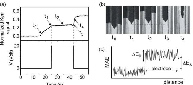
The use of local electrodes on a continuous ferromagnetic layer allows the creation of an MAE step at the edge of the electrode when a voltage is applied. Such energy step may be used to pin DW. Indeed, we observe that the effect of the E-field on DW propagation differs below and at the edges of electrode E2. In Figure 4, the magnetization reversal at a fixed magnetic field of 2.4
mT is recorded as a function of time and while turning the E-field on and off. The integrated Kerr intensity below the electrode and the applied potential are represented as function of time in Figure 4(a) and the corresponding images are shown in Figure 4(b) (see supplementary material for a video).
Fig. 4: (a) Integrated Kerr intensity recorded below the ITO electrode and applied voltage as a function of time for a constant magnetic field of 2.4 mT. (b) Corresponding Kerr images. (c) Schematic representation of the MAE profile below and outside the electrode. The energy step ∆ES and the MAE fluctuations due to local defects ∆EB are represented.
DW propagation below the electrode at t0, is characterized by a progressive increase in the
detected integrated intensity. At t1 the voltage is turned to +20 V and as a result of the increase in
the MAE, the DW velocity decreases by approximately one order of magnitude below the electrode while the DW outside the electrode keeps propagating (Figure 4(b) t1 to t3). Although
the DW below the electrode is only slowed down by the E-field, the DW is pinned at the electrode sides between t1 and t3. We argue that this pinning of the DW is related to the presence
at the edge of the electrode of an energy step ∆ES due to the voltage induced MAE difference
below and outside the electrode (see Figure 4(c)). This energy step can be overcome by thermal fluctuations and as its height is proportional to the E-field, an exponential variation of the pinning time with V is expected. We observe that for V=20 V, the DW is efficiently pinned on the electrode edge at the time scale of our experiment (t∼20s). At t3, the MAE is lowered and the
(last image in Figure 4(c)). This demonstration of an efficient and reversible electrical DW pinning open the way for controlled DW propagation which is essential in future logic or memory applications.
In summary, the results presented here provide a consistent picture of domain wall control in both the nucleation and the propagation regimes using an E-field. The tuning of anisotropy along the wedge allows us to use different local gates on a single sample to either favour DW nucleation below the gate or pin a DW on its edge. Such tuning of the magnetization reversal suggests that magnetic reservoirs and notches, which are respectively used to generate and block DW in nanowires of similar materials, could be advantageously replaced by local gates taking advantage of the tunability of an electric control.
This work was supported by the French National Research Agency (ANR) under the project ANR-2010-BLANC-1006-ELECMADE and the Nanosciences Foundation under the project POMME. The lithography was carried out in the Nanofab cleanroom facilities of Grenoble. The authors thank E. Wagner for technical assistance on the Kerr microscope and M. Darques for his help on image processing.
APPENDIX A : Nucleation simulation
The nucleation probability is defined, following the Néel-Brown model as
( )
(
/)
1 t
P t e− τ
= − where 1 /τ 1/τ0.e(−EN/k TB )
= is the nucleation rate, 1/τ0 =1010 the try rate, EN the energy barrier
and T=300 K the temperature. The image presented in Figure 2(b) right is obtained by a Monte-Carlo simulation on a rectangle where /
N B
E k Tis increasing linearly from bottom to top with
/ 20
N B
E k T = (bottom) and ∆EN /EN=12%. The nucleation process was simulated for a t=1s
slope of the averaged horizontal intensity versus vertical position in the image. In the Kerr image of Figure 2.a left, the nucleation centers present a few micron diameter because the DW have started to propagate. To reproduce these experimental conditions we have also propagated the nucleated centers in the simulation.
APPENDIX B : Gate properties and trapped charges.
The measured capacitances of the electrodes are C∼0.06 µF/cm2. This agrees with an effective dielectric constant εeff∼15 for the Al2O3/HfO2 dielectric bilayer. As observed in Figure 4.e the
effective zero E-field is obtained for V∼-8 V. This indicates the presence of fixed trapped charges in the dielectric. The derived charge density is of 1.5x10¹³e-/cm². Those charges are induced during the deposition of ITO as they are present only below the ITO electrodes inducing a difference in the anisotropy below ITO and outside ITO. Such trapped charges, with the same density, were observed below ITO electrodes all over the sample. Charges traps with similar densities have already been observed in high-k based capacitors containing HfO228 and ZrO229
insulators. REFERENCES
1
R. Ramesh and N. A. Spaldin, Multiferroics: progress and prospects in thin films, Nature Mater. 6, 21 (2007).
2
H. Ohno, D. Chiba, F. Matsukura, T. Omiya, E. Abe, T. Dietl, Y. Ohno, K. Ohtani, Electric-field control of ferromagnetism. Nature 408, 944 (2000).
3
M. Weisheit, S. Fähler, A. Marty, Y. Souche, C. Poinsignon and D. Givord, Electric field- induced modification of magnetism in thin-film ferromagnets Science 315, 349 (2007).
4
S. J. Gamble, M. H. Burkhardt, A. Kashuba, R. Allenspach, S. S. P. Parkin, H. C. Siegmann and J. Stöhr, Electric field induced magnetic anisotropy in a ferromagnet Phys. Rev. Lett. 102, 217201 (2009).
5
T. Maruyama, Y. Shiota, T. Nozaki, K. Ohta, N. Toda, M. Mizuguchi, A. A. Tulapurkar, T. Shinjo, M. Shiraishi, S. Mizukami, Y. Ando and Y. Suzuki, Large voltage-induced magnetic anisotropy change in a few atomic layers of iron Nat. Nano. 4, 158 (2009).
6
M. Zhernenkov, M. R. Fitzsimmons, J. Chlistunoff, J. Majewski, I. Tudosa and E. E. Fullerton, Electric-field modification of magnetism in a thin CoPd film. Phys. Rev. B 82, 024420 (2010).
7
T. Seki, M. Kohda, J. Nitta and K. Takanashi, Coercivity change in an FePt thin layer in a Hall device by voltage application. Appl. Phys. Lett. 98, 212505 (2011).
8
F. Bonell, S. Murakami, Y. Shiota, T. Nozaki, T. Shinjo, Y. Suzuki, Large change in perpendicular magnetic anisotropy induced by an electric field in FePd ultrathin films. Appl. Phys. Lett. 98, 232510 (2011).
9
C.-G. Duan, J. P. Velev, R. F. Sabirianov, Z. Zhu, J. Chu, S. S. Jaswal, and E. Y. Tsymbal, Surface magnetoelectric effect in ferromagnetic metal films. Phys. Rev. Lett. 101, 137201 (2008).
10
K. Nakamura, R. Shimabukuro, Y. Fujiwara, T. Akiyama, T. Ito and A. J. Freeman, Giant modification of the magnetocristalline anisotropy in transition metal monolayers by an external electric field. Phys. Rev. Lett. 102, 187201 (2009).
11
K. Nakamura, T. Akiyama, T. Ito, M. Weinert, and A. J. Freeman, Role of an interfacial FeO layer in the electric-field-driven switching of magnetocrystalline anisotropy at the Fe/MgO interface. Phys. Rev.Lett. 81, 220409 (2010).
12
Y. Shiota, T. Maruyama, T. Nozaki, T. Shinjo, M. Shiraishi and Y. Suzuki, Voltage-assisted magnetization switching in ultrathin Fe80Co20 alloy layers. Appl. Phys. Exp. 2, 063001 (2009). 13
T. Nozaki, Y. Shiota, M. Shiraishi, T. Shinjo, and Y. Suzuki, Voltage-induced perpendicular magnetic anisotropy change in magnetic tunnel junctions. Appl. Phys. Lett. 96, 022506 (2009).
14
S.-S. Ha, N.-H. Kim, S. Lee, C.-Y. You, Y. Shiota, T. Maruyama, T. Nozaki, and Y. Suzuki, Voltage induced magnetic anisotropy change in ultrathin Fe80Co20/MgO junctions with Brillouin
light scattering. Appl. Phys. Lett. 96, 142512 (2010).
15
M. Endo, S. Kanai, S. Ikeda, F. Matsukura and H. Ohno, Electric-field effects on thickness dependent magnetic anisotropy of sputtered MgO/Co40Fe40B20/Ta structures. Appl. Phys. Lett. 96,
212503 (2010).
16
Y. Shiota, S. Murakami, F. Bonell, T. Nozaki, T. Shinjo and Suzuki, Y. Quantitative evaluation of voltage-induced magnetic anisotropy change by magnetoresistance measurement. Appl. Phys. Exp. 4, 043005 (2011).
17
C. Fowley, K. Rode, K. Oguz, H. Kurt and J. M. D. Coey, Electric field induced changes in the coercivity of a thin-film ferromagnet. J. Phys. D Appl. Phys. 44, 305001 (2011).
18
M. Endo, S. Kanai, S. Ikeda, F. Matsukura, H. Ohno, Electric-field effects on thickness
dependent magnetic anisotropy of sputtered MgO/Co40Fe40B20/Ta structures. Appl. Phys. Lett. 96, 212503 (2010).
19
K. Kita, D. W. Abraham, M. J. Gajek and D. C. Worledge, Electric-field-control of magnetic anisotropy of Co0.6Fe0.2B0.2/oxide stacks using reduced voltage. J. Appl. Phys. 112, 033919 (2012).
20
W.-G.Wang, M. Li, S. Hageman and C. L. Chien, Electric-field-assisted switching in magnetic tunnel junctions. Nat. Mater. 11, 64 (2012).
21
Y. Shiota, T. Nozaki, F. Bonell, S. Murakami, T. Shinjo and Y. Suzuki, Induction of coherent magnetization switching in a few atomic layers of FeCo using voltage pulses. Nature Mater. 11, 39 (2012).
22
A. J. Schellekens, A. van den Brink, J. H. Franken, H. J. M. Swagten and B. Koopmans
Electric-field control of domain wall motion in perpendicularly magnetized materials. Nature Comm. 3, 847 (2012).
23
U. Bauer, S. Emori and G. S. D. Beach, Electric field control of domain wall propagation in Pt/Co/GdOx films. Appl. Phys. Lett. 100, 192408 (2012).
24
D. Chiba, M. Kawaguchi, S. Fukami, N. Ishiwata, K. Shimamura, K. Kobayashi and T. Ono, Electric-field control of magnetic domain-wall velocity in ultrathin cobalt with perpendicular magnetization. Nature Comm. 3, 888 (2012).
25
D. Chiba, S. Fukami, K. Shimamura, N. Ishiwata, K. Kobayashi and T. Ono, Electrical control of the ferromagnetic phase transition in cobalt at room temperature. Nat. Mater. 10, 853856 (2010).
26
K. Shimamura, D. Chiba, S. Ono, S. Fukami, N. Ishiwata, M. Kawaguchi, K. Kobayashi and T. Ono, Electrical control of Curie temperature in cobalt using an ionic liquid film. Appl. Phys. Lett. 100, 122402 (2012).
27
A. Manchon, C. Ducruet, L. Lombard, S. Auffret, B. Rodmacq, B. Dieny, S. Pizzini, J. Vogel, V. Uhlir, M. Hochstrasser and G. Panaccione, Analysis of oxygen induced anisotropy crossover in Pt/Co/MOx trilayers. J. Appl. Phys. 104, 043914 (2008).
28
S. Maikap, H. Y. Lee, T.-Y. Wang, P.-J. Tzeng, C. C. Wang, L. S. Lee, K. C. Liu, J.-R. Yang and M.-J. Tsai, Charge trapping characteristics of atomic-layer-deposited HfO2 films with Al2O3 as a blocking oxide for high-density non-volatile memory device applications. Semicond. Sci. Technol. 22, 884889 (2007).
29
U. Bauer, M. Przybylski, J. Kirschner and G. S. D. Beach, Magnetoelectric Charge Trap Memory. Nano Lett. 12, 1437 (2012).
30
P. J. Metaxas, J. P. Jamet, A. Mougin, M. Cormier, J. Ferre, V. Baltz, B. Rodmacq, B. Dieny, and R. L. Stamps, Creep and Flow Regimes of Magnetic Domain-Wall Motion in Ultrathin Pt/Co/Pt Films with Perpendicular Anisotropy. Phys. Rev. Lett. 99, 217208 (2007).