HAL Id: hal-00966955
https://hal.archives-ouvertes.fr/hal-00966955
Submitted on 27 Mar 2014
HAL is a multi-disciplinary open access
archive for the deposit and dissemination of
sci-entific research documents, whether they are
pub-lished or not. The documents may come from
teaching and research institutions in France or
abroad, or from public or private research centers.
L’archive ouverte pluridisciplinaire HAL, est
destinée au dépôt et à la diffusion de documents
scientifiques de niveau recherche, publiés ou non,
émanant des établissements d’enseignement et de
recherche français ou étrangers, des laboratoires
publics ou privés.
Metallization of polymer composites by metalorganic
chemical vapor deposition of Cu: Surface
functionalization driven films characteristics
Thomas Duguet, François Senocq, Lydia Laffont, Constantin Vahlas
To cite this version:
Thomas Duguet, François Senocq, Lydia Laffont, Constantin Vahlas.
Metallization of polymer
composites by metalorganic chemical vapor deposition of Cu: Surface functionalization driven
films characteristics.
Surface and Coatings Technology, Elsevier, 2013, vol.
230, pp.
254-259.
O
pen
A
rchive
T
OULOUSE
A
rchive
O
uverte (
OATAO
)
OATAO is an open access repository that collects the work of Toulouse researchers and
makes it freely available over the web where possible.
This is an author-deposited version published in :
http://oatao.univ-toulouse.fr/
Eprints ID : 11274
To link to this article
: DOI:10.1016/j.surfcoat.2013.06.065
URL :
http://dx.doi.org/10.1016/j.surfcoat.2013.06.065
To cite this version
:
Duguet, Thomas and Senocq, François and Laffont, Lydia and
Vahlas, Constantin Metallization of polymer composites by
metalorganic chemical vapor deposition of Cu: Surface
functionalization driven films characteristics. (2013) Surface and
Coatings Technology, vol. 230 . pp. 254-259. ISSN 0257-8972
Any correspondance concerning this service should be sent to the repository
administrator:
staff-oatao@listes-diff.inp-toulouse.fr
Metallization of polymer composites by metalorganic chemical vapor
deposition of Cu: Surface functionalization driven films characteristics
Thomas Duguet
⁎
, François Senocq, Lydia Laffont, Constantin Vahlas
CIRIMAT, CNRS — Université de Toulouse, 4, allée Emile Monso, BP-44362, 31030 Toulouse Cedex 4, Francea b s t r a c t
Keywords: Metallization MOCVD Cu Epoxy CompositeThe present work is an evaluation of the most efficient pretreatments that are used in the field of metallization of poly-epoxies. In particular, we treat the case of MOCVD metallization with the constraints of limiting preparation steps and non-null, though limited thermal budget, and obtaining smooth, adherent, and highly conductive Cu coatings. Several results are presented after applying ex or in situ mechanical and chemical treatments. For the first time, transmission electron microscopy investigations illustrate the effect on the coating of H2O vapor
addi-tion during the first steps of the deposiaddi-tion process. In an original manner, we show that the enhancement of sur-face reactivity displaces the center of mass of the deposit towards the gas entry in the hot-wall reactor. Additionally, with the particularity of the hot-wall configuration, we show that differences in the deposition con-ditions along the reactor locally place the deposition in different regimes, i.e. diffusional or kinetic, with a strong effect on the coating microstructure and properties. Therefore, for both controlling the film properties and tuning the MOCVD reactor and the processing conditions, surface reactivity must be considered, in addition to the clas-sical macroscopic processing parameters.
1. Introduction
Replacement of metals by polymer-based composites maintains stiffness while providing weight gain, the latter property being critical for energy saves and low environmental impact. Electrical conductivity is often required for polymer composites, and can be obtained by the deposition on their surfaces of a metallic film. Metalorganic chemical vapor deposition (MOCVD) is well suited for treating complex, non-line-of-sight surfaces while avoiding the often eco-unfriendly nature of wet chemicals. Copper, the second metal with the lowest electrical resistivity after Ag, is most often used for this purpose, also because it is abundant, accessible, and presents moderate environmental foot-print. However, due to the relatively low surface energy of polymers in general and epoxies in particular (in the order of 20 to 50 mJ/m2
[1,2], to be compared with 1000 mJ/m2for metals and oxides[3]) nu-merous drawbacks may tarnish the deposition process. These include considerable nucleation delay of Cu, rough, discontinuous morphology of the films and poor adhesion to the substrate. Accommodation of these drawbacks depends among other factors on the surface character-istics of the polymer substrate, and on the deposition chemistry and conditions. Insight in the abundant literature on the metallization of polymers results in typically three ways to circumvent this difficulty, namely by increasing the surface roughness aiming at increasing the mechanical anchoring of the film, and by functionalizing the surface ei-ther by grafting, or by forming reactive groups on it. The latter is often
achieved by oxidizing the non-polar C\C and C\H groups which pre-vail on the surface of epoxies.
There are but few reports evaluating the efficiency of such treatments in the frame of a polymer metallization involving an MOCVD process. This is the topic of the present paper. We report on the influence of ex situ and/or in situ treatments of the surface of polymer composites on the mor-phological characteristics and on the growth rate of Cu films processed by MOCVD from (hfac)Cu(I)(MHY) (Gigacopper®) where (hfac) is hexa-fluoroacetylacetonate and (MHY) is 2-methyl-1-hexen-3-yne[4–6]and from copper(I) N,N′-diisopropylacetamidinate, ([Cu(amd)2])[7,8]. We in-vestigate six surface pre-treatments, namely (i) mechanical polishing and (ii) chemical etching aiming at the formation of a controlled surface roughness and thus enhancement of mechanical anchoring of the metal, (iii) degasing of the composite aiming at desorption of contaminants, (iv) UV photooxidation in air aiming at the replacement of non-polar C\C and C\H bonds by polar O\C = O ones, (v) flush of the substrate with H2O vapors during the first steps of the deposition aiming at the cre-ation of \OH functional groups and at the formcre-ation of a metal oxide in-terphase between the polymer and the pure metal, and finally (vi) the grafting of a thin polydopamine interlayer.
In that which follows, we first present experimental details on the surface preparation of the substrates and on the characterization techniques. Then, we present and discuss the obtained results on the deposition of Cu films, in terms of interfacial characteristics, sur-face morphology, and growth rate as functions of different sursur-face treatments. Finally, we provide concluding remarks and synthetic guidance on the most favorable surface treatments of polymer com-posites in view of their metallization by MOCVD of Cu films.
⁎ Corresponding author. Tel.: +33 534323439. E-mail address:thomas.duguet@ensiacet.fr(T. Duguet).
2. Experimental details
MOCVD experiments are performed in horizontal, hot wall reactors operating at 5 Torr. The deposition protocols have been extensively reported in the literature for Gigacopper® [5] and for [Cu(amd)2]
[7,8]. Processing temperature is 195 °C and 220 °C for deposition from the two precursors, respectively. The use of Cu(amd)2is guided by the need to screen the different surface pre-treatments with a precursor which may achieve the deposition of non-covering but uniform thin films. Actually, although Cu deposition from Cu(amd)2shows a lower growth rate than that of Cupraselect® or Gigacopper®, it can achieve a good thickness uniformity on large areas[9]. These features allow the use of a simple reactor equipped with a sublimator and using re-duced precursor amounts. On the other hand, the study of thick Cu coatings is performed using Gigacopper® which is well-known for its high deposition rate, provided that a DLI-MOCVD system is used. Details on particular processing conditions are reported in the next section. Epoxy matrix carbon fiber reinforced composites with epoxy finished surface are used as substrates. They are cleaned with detergent and acetone, dried with Ar and baked for 45 min at 60 °C for outgasing. Following this systematic pretreatment, the sub-strates are subjected to different treatments either ex situ prior intro-duction in the deposition chamber or in situ, prior Cu deposition. These treatments aim at either increasing surface area, or modifying surface reactivity, or functionalizing the surface. Surface area is in-creased ex situ by mechanical polishing aiming at the formation of a controlled surface roughness and thus enhancement of mechanical anchoring of the metal. Two finish roughnesses are thus created, obtained by polishing with P1200 (rough) and P4000 (smooth) grit SiC paper. For similar purpose, roughness is also obtained by chemi-cal etching of the surface by immersion for 10 min at 80 °C in an al-kaline oxidizing aqueous solution containing 55 g/L of KMnO4and 1.2 mol/L of NaOH. Modification of surface reactivity is achieved by UV photooxidation in air at 76 °C for 2 h aiming at the replacement of non-polar C\C and C\H bonds by polar O\C = O ones. Alterna-tively, an in situ treatment consists in flushing the substrate with H2O vapors during the first steps of the deposition, aiming at the creation of \OH functional groups and at the formation of a metal oxide in-terphase between the polymer and the pure metal. This is achieved by bubbling 50 standard cubic centimeters per minute (sccm) of N2 through water maintained at 3 °C. Finally, surface functionalization is attempted by immersing the substrates in a buffer solution of 10 mM TRIS-HCl (pH 8.5) prepared with deionized water, and next introducing 2 mg/mL of dopamine˙HCl (Sigma Aldrich®)[10]. Sam-ples are then left for 24 h with gentle mechanical stirring and are fi-nally rinsed thoroughly with deionized water and dried with Ar. This mussel-inspired functionalization aims at forming a polydopamine (DOPA) film on the composite substrate prior introduction in the CVD reactor. It has been successfully applied in various systems in-cluding metallization of DOPA-modified rubber elastomers [11], and DOPA-modified poly-epoxy[12]. However, it has never been ap-plied to a thermally activated process such as CVD.
Cross-sections of samples processed using H2O are prepared for TEM analysis, by cutting thin slices, normal to the film/substrate interface with a diamond wire saw. Two slices are glued together, film to film and embedded in a 3 mm diameter brass tube in epoxy resin. After cur-ing, the tube is sectioned into approximately 300 μm thick disks. These disks are then polished on both faces and cut with a diamond knife to create the pyramid shape. Electron transparent samples are subse-quently obtained by preparing thin foils using diamond ultramicrotomy and deposited on lacey-carbon-film coated copper grids. TEM and HRTEM investigations are performed using a JEOL JEM 2100 microscope operating at 200 kV and equipped with an energy dispersive spectrom-eter (EDS) for chemical analysis. The diffraction patterns of the investi-gated materials are obtained using the selected area electron diffraction (SAED) mode or by Fourier transform of the HRTEM images.
For the results presented inFig. 4, thickness of the Cu films is eval-uated through the evolution of the intensity of the diffracted X-Ray beam as a function of the incidence angle of the incoming beam
[13]on 50 × 10 mm2samples. According to the adopted model, the diffracted intensity, for a given line, can be expressed by the relation: I ¼ K sinΩ ! " " 1− exp − μρ # $ " !sinΩ1 "þ sinβ1 # $ # $ "ρ "d h i # $ h i μ ρ # $ " !sinΩ1 "þ sinβ1 # $ # $ "ρ h i
where Ω is the incident angle of the incoming beam related to the flat surface of the sample, β the angle of the diffracted beam related to the sample surface, μ/ρ the mass absorption coefficient for the film, ρthe density of the film and d its thickness. K is a factor which takes into account the intensity and section of the incoming X-Ray beam, the experimental factors, i.e. divergence of the slits, dimension of the irradiated section of the sample in the perpendicular direction of the diffractometer axes (which have to be constant along the sam-ple for one set of measurements), and structure factor for the consid-ered diffraction line. Provided these experimental factors are kept constant, a set of acquisitions for the same diffraction line at different incident angles, yields a I = f (Ω) curve whose equation can provide a good estimation of the thickness of the sample. The main limitation of the method is that it is more accurate for thin samples. In the pres-ent case, calculated thicknesses over 6–7 μm are underestimated as the variations of the I = f (Ω) curves with thickness are very weak above these values. Additionally, we assume that the copper films have the bulk density of 8.92 g/cm3. We performed measurements in the 42.3–43.3 2θ range (±1° around Cu 111 line), with a Bruker D8 Da Vinci, fitted with a Lynx Eye detector, Cu Kα radiation, 0.1° di-vergence slits, and in a Ω range from 1 to 20°.
X-ray photoelectron spectroscopy is performed with a monochro-matic Thermo Scientific K-alpha for the investigation of the influence of ex situ UV treatment of the surface. Surface and cross section mor-phologies, and chemical composition are investigated with a scanning electron microscope (SEM) (LEO 435 VP) equipped with a Ge detector (Imix-PC, PGT) and an ultrathin window for the detection of light ele-ments by energy dispersive X-ray spectroscopy (EDX). Electrical resis-tivity is measured in selected films with a Signatone 4-point probe resistivity meter.
3. Results and discussion
Fig. 1 shows surface SEM images of Cu films processed from [Cu(amd)2] on the polymer composite that has been pretreated in three different ways: mechanical polishing with a P4000 fine grade SiC paper followed by UV irradiation for 2 h (1a), mechanical polishing with a P1200 coarse grade SiC paper followed by UV irradiation for 2 h (1b), and chemically etched following the alkaline oxidizing pretreatment (1c). In the three micrographs, the Cu film appears as a fine, granular su-perstructure on the composite pattern. Despite the decrease of charging effects obtained by metallization, the quality of the micrographs is rela-tively poor. Indeed, the aimed observation of the ultra-thin Cu film does not allow application of a pronounced metallization. It is worth noting that both chemical etching and polishing with a coarse grade lead to the uncovering of the C-fibers, whereas fine polishing maintains the epoxy surface layer. When smoothness of the metallic coating is required, the latter gentle pretreatment should be favored. Additionally, surface rough-ness and morphology due to wet chemistry differ from that due to polishing. The former rather creates sub- or micro-metric pores pointing towards the bulk of the substrate[14–16]whereas mechanical polishing scratches the surface and spreads epoxy debris in the polishing directions. For mechanical anchoring of the metallic coating, we assume that chemical etching may be more efficient. However, despite the obvious mechanical locking which would result from the metallization of rough surfaces, the uncovering of C-fibers by coarse polishing or
chemical etching is not satisfactory when smooth Cu films are targeted. Indeed, such severe pretreatments provide heterogeneous surfaces, where the reactivity of C-fibers and of epoxy areas are different, resulting in different growth rates of the Cu film. Consequently, the obtained coat-ing is rough revealcoat-ing the C-fibers network as it can be seen in the bottom photograph ofFig. 2. If chemical etching is to be used with the epoxy of this study, an optimization of the etching time – and probably the intro-duction of swelling and reducing steps – would be essential.
UV irradiation of samples was performed with the aims to oxidize the surface and to increase the surface energy[17]by creating reactive functional groups at the surface of poly-epoxies and graphite[18,19].
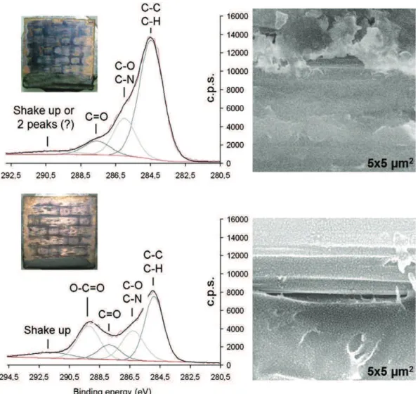
Fig. 2shows the XPS C1s core-level spectra of as received (top) and UV cured (bottom) P1200 polished surfaces, along with photographs
and SEM surface micrographs of the resulting Cu films processed from Cu(amd)2 in the same deposition run. SEM was performed in the same conditions for both samples. These include same sample holder, working distance, probe current, high voltage, and adjustment settings. Preferential growth of the Cu film on the periphery of both samples is observed in the photographs; it is attributed to edge effects and to to-pological defects at these areas, resulting in increased reactivity. Macro-scopically, the effect of the UV pretreatment provides a brighter, metallic Cu film. Observation of the central surface area reveals that Cu covers the pretreated surface more uniformly than the bare surface. Operation of SEM and observation of the obtained images confirm this difference. Indeed, charging effects and the loss of imaging resolution on the untreated sample indicate that significantly less Cu is present compared to the UV cured sample. The SEM surface micrograph corre-sponding to the latter sample shows Cu particles of uniform size which are homogeneously distributed on the surface, regardless of the underlying material; i.e. carbon fibers or poly-epoxy. The UV treatment on smoothly (P4000) polished surface further enhances the uniformity of the Cu film (Fig. 1a).
Insight in the effect of the UV treatment on the composite surface is obtained by XPS spectroscopy. C1s core-level spectra are presented in
Fig. 2. The analysis of the C1s peak is performed after a Shirley-type background subtraction and calculated as the convolution of a Gaussian and a Lorentzian with its associated fitting parameters such as a full width at half maximum, asymmetry parameter, energy intensity and position. Identification of the different contributions is based on litera-ture information[18,20–22]. We observe a large decrease of the intensi-ty of the aliphatic carbon (C\C, C\H) at 284.6 ± 0.1 eV, along with the increase of the relative contributions of oxidized species and the forma-tion of a new contribuforma-tion at ca. 289 eV. The latter peak is due to the cre-ation of \COOR functional groups which can most likely be carboxylic acids of the form R\C(_O)\OH, or esters of the form R\C(_O)\OR. It is concluded that UV treatment results in the oxidation of the surface and in the creation of reactive functional groups. The surface energy is thus increased and subsequently the wettability of the surface by the or-ganometallic precursor is also increased. Enhanced wettability favors homogeneous nucleation of Cu and hence uniform surface coverage by Cu. These effects are visible both macro- and microscopically.
An alternative method to enhance the chemical adhesion is the introduction of water vapors during the initial growth steps of the film[23,24]. This method aims at the formation of copper oxide at the epoxy/Cu interface that shows improved chemical affinity to-wards the epoxy. It is applied in the realization of Cu/epoxy joints, where the proper Cu oxidation is performed before epoxy polymeri-zation. The low-T cuprous oxide Cu2O shows the best chemical adhe-sion to epoxy[25–27]. The use of water vapor and proper cooling during CVD of Cu results in decrease of the nucleation delay and bet-ter adhesion[5,24]. A better adhesion can also be achieved by apply-ing post-deposition annealapply-ing in air[28]. A significant advantage of this method is that the water vapor treatment is easily implemented in a CVD process and allows treating complex surface geometries.
Insight in the epoxy-Cu interface is realized by TEM. Dedicated de-position experiments from Gigacopper® (flow rate = 0.20 g/min) are performed in this purpose, where the surface of the polymer composite was just cleaned. A thick Cu film is cut at coordinate [+60] of the sam-ple presented inFig. 5.Fig. 3a is a bright field image of the entire cross section of the Cu film. It reveals that the film is composed of two parts: a 0.3 μm-thick sublayer at the interface with the composite and a 2.2-μm thick, outer one. The latter systematically yields selected area electron diffraction (SAED) patterns characteristic of a single crystallite, as shown inFig. 3b. These patterns are indexed as the face-centered cubic Cu of space group Fm3m and lattice parameter a = 3.615 Å. The preferential growth direction of the pure copper crystallite analyzed here is [001]. Due to the high thickness of the cross section in this area, the 0.3 μm-thick sublayer appears in dark contrast. For this reason, the SAED pattern of this part of the film shown inFig. 3c has been
Fig. 1.Top-view SEM images of the fine granular superstructure of Cu deposited by MOCVD from [Cu(amd)2] on (a) a surface polished with P4000 grade SiC paper, (b) a surface polished with P1200 grade SiC paper, and (c) a surface etched for 10 min at 80 °C in an alkaline oxidizing aqueous solution containing 55 g/L of KMnO4 and 1.2 mol/L of NaOH.
obtained on a thinner region. This pattern is composed of concentric rings corresponding to a polycrystalline sample and is indexed using the Cu2O lattice which has a cubic structure (space group Pn3m) with lattice parameter a = 4.258 Å. The high resolution HRTEM image performed in this region (Fig. 3d) presents Cu2O nanocrystals whose size varies between 5 nm and 15 nm. The mechanism that leads to the formation of Cu2O is not clear yet. We assume that either the CuI precursor is modified by water in the gas phase and the Cu oxide is di-rectly deposited, or pure Cu0is deposited and further oxidized by water on the growing surface.
Considering that surface pretreatments enhance the reactivity of the composite substrate, one expects that on appropriately function-alized surfaces limiting steps would be easier to overcome, thus allowing for (a) a more efficient contribution of the reactive gas phase to the overall growth rate and also (b) a finer microstructure of the film. Such limiting steps can be nucleation delay and nucle-ation density, ultimately leading to the formnucle-ation of a continuous film. An expected consequence of an efficient contribution of the re-active gas phase to the overall growth rate would be a shift of the thickness profile towards the gas entry of the horizontal, hot wall re-actor and a steeper decrease of the thickness towards the end of the deposition zone due to larger precursor depletion. Conversely, by evaluating the characteristics of the thickness profile of the film in constant processing conditions for different surface pretreatments one would conclude on the relative efficiency of the latter.
Fig. 4shows the thickness of the Cu coating for different surface pre-treatments, evaluated by XRD, as a function of the longitudinal position in the isothermal section of the reactor. Depositions are performed with a 0.05 g/min flow rate of Gigacopper® into the deposition chamber. The direction of the precursor flux is shown schematically by a black arrow. The baseline corresponds to the thickness of Cu deposited on the untreated (bare) surface. This baseline is relatively flat with thicknesses between 2.8 and 2.1 μm.
The thickness of Cu films processed on H2O, UV, and KMnO4treated surfaces present clear tendencies; i.e. large thicknesses from 5 μm to higher than 7 μm at the gas entry and drastic decrease towards the exit of the reactor. The strong effect of KMnO4compared with the UV and H2O treatments is attributed to the creation of roughness whereas the two other treatments enhance chemical reactivity. Higher rough-ness in the present treatment conditions results in strong increase of the reactive surface area. It is worth noting that finally, DOPA including treatments show reduced even null efficiency. We suspect that the polydopamine film does not sustain the 195 °C deposition temperature, and then creates a partial pressure of outgasing products above the sample which prevents the proper Cu deposition. Depositions at 185 °C give similar results (not shown). To our knowledge, there is no study of the durability of polydopamine films with temperature, an im-portant feature of the MOCVD process.
Considering constraints of treating complex geometries and follow-ing the above results, we select the in situ H2O treatment and study a Cu
Fig. 2.XPS C1s spectra of 10 × 10 mm2composite substrates polished with P1200 grade SiC paper and photograph and top-view SEM micrograph of the deposited Cu film. Top: As-received. Bottom: UV cured prior introduction in the MOCVD reactor.
coating that has been deposited on a 180 × 20 mm2composite sub-strate. Deposition is performed by injecting 0.20 g/min of Gigacopper®, with water vapor feeding the deposition chamber during the first 2 min (50 sccm N2(g)bubbling in 3 °C-water).Fig. 5summarizes the obtained results. The substrate is positioned with its long side parallel to the axis of the reactor with its lateral coordinates [− 10] and [+ 10] in contact with the reactor walls, where Cu deposition also occurs. The longitudi-nal coordinate [0] corresponds to the beginning of the isothermal sec-tion of the reactor which covers 70 mm. In situ measurements of temperature were performed in the adopted conditions of Cu deposi-tion at coordinates [− 60], [0], and [+ 60] and the results are reported in the upper part ofFig. 5. Deposition occurs in an increasing tempera-ture gradient in the range [− 90; 0], in an isothermal section in the range [0; +70], and in a decreasing gradient in the range [+70; +90]. The maximum thickness (19 μm) is found at coordinate [0, 0]. From this point Cu thickness decreases in the lateral and longitudinal directions, in good agreement with the results obtained by XRD, shown inFig. 4.
The histogram in the middle ofFig. 5summarizes results of the electrical properties of the film measured at different positions across the length of the substrate. Sheet resistance Rs= U/I and re-sistivity ρ = Rs. C.t, where C is a geometrical factor and t the film thickness [29], are presented based on the same 4-point probe data. The lowest sheet resistance is found for the thickest films at co-ordinates [0] and [+30]. The lowest resistivity is found for thinner films at coordinates [− 45] and [+ 60]. Resistivity depends mainly on the Cu purity and structural defects such as the grain boundary density. Cu purity is systematically checked, and within the limits of the EDX spectrometer all the samples are free of heteroatoms (namely C, O, F). Therefore, it is likely that either the temperature and/or the molar fraction of precursor that prevail at coordinates [0] and [+30] favor(s) the formation of defects. In contrast, lower temperature and lower precursor concentration corresponding to positions [− 45] and [+ 60], respectively, favor the deposition of a more electrically conductive film. Part of the answer is provided by
Fig. 3.TEM investigation of the interface between the composite substrate and the Cu film processed using water vapor during the first steps of growth. Cu is deposited with a 0.20 g/min flow rate of Gigacopper. (a) Bright field image with the different SAED areas schematically circled. (b) Diffraction pattern obtained in the Cu coating along the [110] zone axis. (c) Diffraction pattern of Cu2O nanocrystals. (d) HRTEM image of Cu2O nanocrystals. (c) and (d) were taken in a thinner region of the TEM sample not corresponding to the one ofFig. 1a.
Fig. 4.Cu coating thickness determined by mean of XRD as a function of the longitudinal position of the surface inside the isothermal section of the reactor, for different surface preparations.
Fig. 5.Top: Thickness profile determined by 30 measurements on SEM cross-sections. Middle: Resistivity and sheet resistance measured by the 4-point probe method. Bottom: Cross section SEM images at the indicated coordinates. Gas flux direction from [−90] to [+90].
the bottom SEM cross sectional images ofFig. 5, corresponding to co-ordinates [− 45], [0] and [+ 60]. At [− 45], we observe a film which covers the surface uniformly over the 20 mm in width, and also con-forms into the concave defect. The film at coordinate [0] is rougher and presents large thickness variations. At coordinate [+60], the film is rougher than at [− 45] but smoother and thinner than at [0]. It seems that the low temperature of coordinate [− 45] locally places deposition in the kinetic regime. Temperature is higher (and equal) at [0] and [+60], probably corresponding to a deposition regime lo-cally controlled by gas phase diffusion and resulting in a microscop-ically rough film. Hence, the thickness difference between [0] and [+60] can only be explained by the depletion of the precursor molar fraction and thus by a decrease of the growth rate. Overall, we attribute the high resistivity at position [0] to defects induced by the large thickness variations. Since the film is rough but thinner at [+60], the resistivity is lower. A satisfactory resistivity is also obtained for the smooth and uniform film at [−45].
4. Conclusions
Microstructure, growth characteristics and electrical properties of MOCVD Cu films on polymer composites depend on the surface treat-ment prior deposition. A treattreat-ment including in situ H2O vapor flush of the sample in processing conditions during the first minutes of the deposition of Cu provides smooth and highly conductive films. Its effect on the applied deposition conditions can be the creation of a Cu2O layer between the substrate and the Cu coating. The main advantage of this treatment is that it can be used as an all-in-one treatment that circum-vents the problem of mechanical polishing or chemical etching that cre-ates a detrimental roughness if not very well mastered. Nevertheless, dedicated characterizations are necessary to evaluate the effect of this treatment on the adherence of the Cu film on the composite surface. The other treatments (UV, KMnO4, DOPA and combination thereof) are obviously efficient but not particularly compatible with the con-straints (mainly thermal) of a MOCVD process applied to complex sur-face geometries.
Traditionally, deposition in a CVD reactor is modeled by a thermo-kinetic law that varies with deposition parameters, such as the precur-sor molar fraction, gas fluxes, temperature, and pressure. Additionally, with the particularity of the hot-wall configuration, differences in the deposition conditions along the reactor locally place the deposition in different regimes, i.e. diffusional or kinetic, with a strong effect on the coating microstructure and properties, as it is shown inFig. 5. In addi-tion and in an original manner, we show that the enhancement of sur-face reactivity displaces the center of mass of the deposit towards the gas entry in the hot-wall reactor. Hence, it plays an important role in the deposition process. Therefore, in order to establish the complete process–structure–properties relationship on a given system, surface reactivity has to be implemented in the model, in addition to the tradi-tional precursor molar fraction–T–P–Fluxes parameters.
Acknowledgments
The DIRECCTE Midi-Pyrénées is acknowledged for financial support. Authors are thankful to P. Doppelt and F. Karmous (CNRS — Université Paris 13) for fruitful discussions and chemical syntheses. Authors are also grateful to J. Esvan (CNRS, Toulouse) for XPS measurements and advice on data analysis. TEM was performed at University of Toulouse at the TEMSCAN Service (Toulouse, France).
References
[1] F. Garbassi, M. Mora, E. Occhielo, Polymer Surfaces: From Physics to Technology, John Wiley and Sons, Chichester, 2002, pp. 169–206.
[2] http://www.surface-tension.de/solid-surface-energy.htm.
[3] N. Eustathopoulos, M.G. Nicholas, B. Drevet, in: R.W. Cahn (Ed.), Wettability at High Temperatures, Pergamon, Amsterdam, 1999, pp. 148–174.
[4] T.Y. Chen, J. Vaissermann, E. Ruiz, J.P. Sénateur, P. Doppelt, Chem. Mater. 13 (2001) 3993–4004.
[5] M. Joulaud, C. Angekort, P. Doppelt, T. Mourier, D. Mayer, Microelectron. Eng. 64 (2002) 107–115.
[6] P. Doppelt, (CNRS, Paris, France) Novel Copper (I) precursors for chemical deposit in gas phase of metallic copper, Patent# WO98/40387, (1998).
[7] V. Krisyuk, L. Aloui, N. Prud'homme, S. Sysoev, F. Senocq, D. Samélor, C. Vahlas, Electrochem. Solid-State Lett. 14 (2011) D26–D29.
[8] A. Turgambaeva, N. Prud'homme, V.V. Krisyuk, C. Vahlas, J. Nanosci. Nanotechnol. 11 (2011) 8198–8201.
[9] I.G. Aviziotis, N. Cheimarios, C. Vahlas, A.G. Boudouvis, EUROCVD19, Surface and Coatings TechnologyVarna, Bulgaria, 2013, (to be submitted).
[10] H. Lee, S.M. Dellatore, W.M. Miller, P.B. Messersmith, Science 318 (2007) 426–430.
[11] W. Du, H. Zou, M. Tian, L. Zhang, W. Wang, Polym. Adv. Technol. 23 (2012) 1029–1035.
[12]D. Schaubroeck, E. Van Den Eeckhout, J. De Baets, P. Dubruel, L. Van Vaeck, A. Van Calster, J. Adhes. Sci. Technol. 26 (2012) 2301–2314.
[13]G.A. Battiston, R. Gerbasi, in: G. Cappuccio, M.L. Terranova (Eds.), Thin Film Char-acterization by Advanced X-Ray Diffraction Techniques, INF-LNF, Frascati, 1996.
[14]J. Ge, R. Tuominen, J.K. Kivilahti, J. Adhes. Sci. Technol. 15 (2001) 1133–1143.
[15]S. Yoon, H.-J. Choi, J.-K. Yang, H.-H. Park, Appl. Surf. Sci. 237 (2004) 451–456.
[16] S. Siau, A. Vervaet, L. Van Vaeck, E. Schacht, U. Demeter, A. Van Calster, J. Electrochem. Soc. 152 (2005) C442–C455.
[17]J. Ge, M.P.K. Turunen, J.K. Kivilahti, Thin Solid Films 440 (2003) 198–207.
[18]S. Vidal, F. Maury, A. Gleizes, Y. Segui, N. Lacombe, P. Raynaud, Plasma Polym. 5 (2000) 15–29.
[19]M. Charbonnier, M. Romand, Int. J. Adhes. Adhes. 23 (2003) 277–285.
[20]A. Hartwig, G. Vitr, V. Schlett, Int. J. Adhes. Adhes. 17 (1997) 373–377.
[21]B.-S. Lee, T. Motoyama, K. Ichikawa, Y. Tabata, D.-C. Lee, Polym. Degrad. Stab. 66 (1999) 271–278.
[22]S.-K. Ryu, B.-J. Park, S.-J. Park, J. Colloid Interface Sci. 215 (1999) 167–169.
[23]A.V. Gelatos, R. Marsh, M. Kottke, C.J. Mogab, Appl. Phys. Lett. 63 (1993) 2842–2844.
[24]C. Marcadal, E. Richard, J. Torres, J. Palleau, R. Madar, Microelectron. Eng. 37–38 (1997) 97–103.
[25]H.K. Yun, K. Cho, J.H. An, C.E. Park, J. Mater. Sci. 27 (1992) 5811–5817.
[26]P.W.K. Chung, M.M.F. Yuen, P.C.H. Chan, N.K.C. Ho, D.C.C. Lam, 52nd Electronic Components & Technology Conference, 2002 Proceedings, 2002, pp. 1665–1670.
[27]K.W. Cho, E.C. Cho, J. Adhes. Sci. Technol. 14 (2000) 1333–1353.
[28]J.J. Eisch, J. Laskowski, J. Bielinski, M.P. Bolesławski, J. Mater. Sci. Lett. 14 (1995) 146–147.