Commercial Assessment of Roll to Roll Manufacturing of Electronic Displays By
Michael Aaron Randolph
B.S., Mechanical Engineering Tennessee Technological University, 2005
Submitted to the Department of Materials Science and Engineering in Fulfillment of the Requirements for the Degree of
Master of Engineering in Materials Science and Engineering
at the
Massachusetts
Institute of Technology September
2006
@ 2006 Massachusetts Institute of Technolo
MASSACHUSETTS INSTITT'
OF TECHNOLOGY
OCT 0
2
2006
LIBRARIES
All Rights ReservedSignature of Author ... <,.-• .-. ..,... .. .. ...
Department of Materials Science and Engineering June 28, 2006
Certified by ... V.... ladimir Bulovic Associate Professor of Electrical Engineering and Computer Science Thesis Supervisor
Certified by... ..-.1- "'V" SEugene A. Fitz erald
Professor of Materials Science and Engineering Thesis Reader
A ccepted by ... ... .. ... . ...-. ... -. ,- .,
Samuel M. Allen POSCO Professor of Physical Metallurgy Chairman, Departmental Committee on Graduate Students
Commercial Assessment of Roll-to-Roll Manufacturing of Electronic Displays by
Michael A. Randolph
Submitted to the Department of Materials Science and Engineering on June 28, 2006 in Fulfillment of the Requirements for the Degree of
Master of Engineering in Materials Science and Engineering ABSTRACT
The cost of manufacturing electronic displays currently limits the range of applications and markets into which it is currently economically feasible to adopt displays. Roll-to-roll manufacturing has been identified by the display industry as a new and
fundamentally different manufacturing paradigm that has the potential to significantly reduce the manufacturing cost of a display relative to the conventional approaches used in the industry. This manufacturing cost reduction could have a profound impact on the display industry by not only transforming the display manufacturing infrastructure, but also by permitting electronic displays to penetrate new markets. The purpose of this thesis is to determine how roll-to-roll manufacturing technology could develop and to assess what impact the technology could have on the electronic display manufacturing industry.
This work first identifies the material, patterning, and equipment technologies that need to come together in order for roll-to-roll manufacturing to be industrially feasible, and then determines how and if the technology will offer a cost reduction over conventional manufacturing techniques. Next, the markets for displays are segmented and analyzed to discern whether niche initial markets exist where roll-to-roll could have a distinctive advantage and gain traction. Competitive technologies such as LCD and modular LED are discussed and it is determined that roll-to-roll displays must compete with LCD technology on the basis of price in the markets in which LCD has incumbency in order to achieve widespread adoption. The display industry structure is analyzed by means of an assessment of the supply chain, intellectual property landscape, financing mechanisms, and business models to understand how partnerships and financial investment risk are salient aspects of the commercialization process. It is concluded that materials cost advantages over current manufacturing approaches and the timing of roll-to-roll technology integration developments relative to the incremental manufacturing cost decreases in competing technologies will ultimately dictate the success of roll-to-roll manufacturing.
Thesis supervisor: Vladimir Bulovic
Acknowledgements
I would like to thank Professor Vladimir Bulovic for his support, interest, and advice throughout the past year. Professor Bulovic empowered me with resources and contacts that provided a fitting balance between academia and industry in my thesis. His dedicated involvement in my work made the learning experience rich and comprehensive, and I could not have asked for a better advisor.
I must also express grave appreciation to Professor Eugene Fitzgerald for
providing the conceptual and analytical tools that are needed to understand how technologies move from the lab bench into industry. The vision and insight that he offered was monumental in enabling me to see through the clouds of information that I had gathered and put structure to ambiguity in order to get down to the core issues that are driving the development of roll-to-roll technology.
Additionally, I must extend multiple thanks to Gerry Chen for his time and the in-depth knowledge that he imparted to me on this subject. Thanks to Greg Moeller and the
QD Vision team, Liz Ziepniewski of I.T. Strategies, and all of the people I met at
conferences, trade shows, and seminars who provided the countless conversations that truly allowed me to see the big picture. I would like to thank the MIT Center for Integrated Photonic Systems (CIPS) for providing the funding for this work.
Finally, I would like to thank my family and friends for giving me the intangible things that made me smile throughout the entire experience.
Table of contents
Acknowledgem ents... 3 Table of contents... 4 List of figures... 6 1 Introduction to Roll-to-Roll... 7 1.1 Background ... 7 1.2 Thesis Scope ... 82 Research and Technology A ssessm ent ... 10
2.1 M aterials ... 10
2.1.1 Supporting M aterials... 11
2.1.1.1. Properties that favor Stainless Steel substrates... 13
2.1.1.2. Properties that favor Plastic Substrates... 15
2.1.1.3. Conclusions: Stainless Steel vs. Plastic Substrates... 15
2.1.2 Functional M aterials ... 16
2.1.2.1. The Front Plane... 16
2.1.2.2. TFT Backplanes ... 20
2.2 Patterning Techniques... 21
2.2.1 Evaporation ... 22
2.2.2 Direct Contact Printing ... 23
2.2.3 Inkjet Printing ... 25
2.2.4 Therm al Transfer ... 27
2.3 Equipm ent and Facilities... 28
2.4 Cost M odeling... 30
2.5 Conclusions from Technology A ssessm ent... 34
2.5.1 M aterials ... 35
2.5.2 Patterning Techniques... 35
2.5.3 Equipm ent and Facilities... 36
3 M arkets and Application Areas ... 37
3.1 Application Areas and M arket Segm entation... 37
3.2 Initial M arkets for R2R M anufactured D isplays ... 41
4 Com petitive and Com plem entary Technologies... 44
4.1 Com petitive Technologies ... 44
4.1.1 Liquid Crystal Displays (LCD s) ... 44
4.1.2 M odular Light Em itting Diodes (LED s)... 47
4.1.3 Paper/Paint... 49
4.1.4 Electrotextiles ... 51
4.2 Com plem entary Technologies ... 55
4.2.1 Flexible Electronics ... 55
4.2.2 OLED ... 55
5 Industry Structure and Business M odels... 57
5.1 Understanding the Supply Chain ... 57
5.2 Intellectual Property Landscape... 60
5.2.1 M aterial Level... 60
5.2.3 Equipm ent Level... 62
5.3 Financing Approaches ... 62
5.4 Business M odels ... 64
5.4.1 E Ink... 64
5.4.2 V itex System s ... 66
5.5 Strategies for Com m ercialization ... 67
6 Conclusions... 69
Appendix... 72
A Cost M odel Details ... 73
Process Flow for Active Matrix Cost Model developed by Abbie Greg, Inc... 73
B ROI M odel by I.T. Strategies... 75
POP Signage ROI M odel... 75
List of figures
Figure 1-1 R2R Manufacturing Concept ... 8
Figure 2-1 Layers Comprising an Active Matrix LCD (AM-LCD) and Active Matrix Organic LED (AM-OLED) display [] ... 11
Figure 2-2 Substrate Comparison [] ... 12
Figure 2-3 E-Ink Display Technology [] ... 18
Figure 2-4 E-Ink Device Structure [15]... 19
Figure 2-5 Patterning Techniques [] ... 22
Figure 2-6 HP Imprint Lithography [27] ... 24
Figure 2-7 Litrex Inkjet System [] ... 26
Figure 2-8 LITI Process [25] ... 27
Figure 2-9 Applied Films SMARTWEB Equipment [] ... 28
Figure 2-10 Cost per square foot vs. Volume [] ... 31
Figure 2-11 Cost Structure of Active Matrix R2R Line [38]... 32
Figure 2-12 Comparison of Batch and Roll-to-Roll Backplane Costs [35]... 33
Figure 3-1 Display Market Segmentation and Size [40] ... 38
Figure 3-2 Applications for Flexible Displays [40]... 39
Figure 3-3 Annual Flat Panel Display Revenues and Growth [43] ... 40
Figure 3-4 Expected Market Adoption Timeline [] ... 41
Figure 4-1 Evolution of LCD Performance [26]... 46
Figure 4-2 LED Display at Turner Staduim ... 48
Figure 4-3 Sony Reader ... 51
Figure 4-4 Functionality for Electrotextiles [50]... 52
Figure 4-5 Woven Display [] ... 54
Figure 5-1 Supply Chain Structure ... 57
CHAPTER
1
Introduction to Roll-to-Roll
1.1 Background
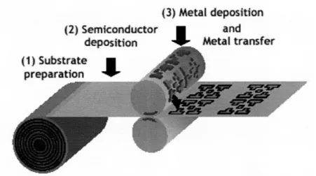
Roll-to-roll (R2R) processing has been identified by the display industry as a technology that could significantly reduce the costs associated with manufacturing displays. Roll-to-roll manufacturing can be most easily conceptualized as the process by which low cost products such as labels and newspapers are currently produced, where thousands of square feet of printed material can be printed for just a few cents. Although electronic display materials are much more expensive than newspaper materials, the R2R printing process itself is inherently low cost and extremely scalable. Industry efforts to achieve R2R manufacturing aspire to implement more arcane materials and controls into this fundamentally mundane process in order to realize order of magnitude reductions in the display manufacturing cost structure. If each layer of a display could be patterned onto a roll of substrate in a continuous deposition process, then it could be possible to realize a profound decrease in the cost of manufacturing an electronic display relative to the conventional approaches used in the industry.
The basic concept of R2R can be illustrated by Figure 1-1, where a functional layer is transferred onto a substrate by contacting the surface to a patterned roll that contains the layer material in an ink form. Although this direct contact printing is one approach to achieve a R2R compatible deposition, there are other additive approaches that are compatible with roll-to-roll processing such as ink jet printing or laser patterning.
(3) Metal deposition (2) Semiconductor
deposition (1) Substrate
preparation
Figure 1-1 R2R Manufacturing Concept
The fundamental difference between roll-to-roll manufacturing and the manufacturing approaches currently used in the display industry is that R2R is a web process whereas the conventional display manufacturing techniques utilize batch processes. This allows the layers and processing operations to be applied to the display continuously as it is moved through the manufacturing facility. The cost reductions are expected to be derived primarily from a reduction in the material handling cost of moving the work-in-progress inventory from process to process within a plant. Additionally, if additive patterning techniques can be used in the R2R process then it is conceivable that a reduction in the cost of materials could also be achieved.
1.2 Thesis Scope
The scope of this work is to assess the commercial potential of roll-to-roll manufacturing in the context of its application to the display industry. This work offers insights on the commercialization process and how roll-to-roll manufacturing could develop from the lab bench to a full scale manufacturing facility. Firstly, this entails the
identification of the technology pieces that need to come together in order for R2R to be implemented into a manufacturing facility, and how and if these can coalesce to realize a reduction in manufacturing costs compared to conventional approaches in the industry (Chapter 2). Second, the display market is segmented and applications for the technology are identified, including an assessment of initial markets where R2R could have a
distinctive advantage (Chapter 3). Next, the thesis builds on this understanding of the marketplace by evaluating the competitive technologies that R2R will encounter in the markets, and also identifies technologies that will complement the development of R2R (Chapter 4). The display industry structure is then analyzed, including an assessment of the supply chain, intellectual property landscape, financing mechanisms, and business models, to draw inferences about successful strategies for commercialization of R2R technologies (Chapter 5). Finally, based on a broad understanding of the technology and industry, conclusions are made about the commercial potential of roll-to-roll
CHAPTER
2
Research and Technology Assessment
The three areas of research that are critical to the development of roll-to-roll manufacturing are advancements in materials, patterning techniques, and equipment. These are the three technology pieces that must be in place in order for roll-to-roll
fabrication of displays to be utilized by industry. It should also be noted that much of the research that is critical to the commercial enabling of R2R is not explicitly labeled as R2R research. For example, a large component of the research related to flexible substrates is carried out for mobile applications. Although the development of flexible substrates is considered to be essential to the advancement of R2R, many of the
endeavors in this area are focused only on its application to mobile devices. Similarly, many other areas of research that are fundamental to the commercial success of R2R may be disguised or categorized in terms of a more narrowly defined application or device structure.
2.1 Materials
There are two main types of materials that are used in the manufacturing of a display: the supporting materials and the functional materials. The supporting materials are static layers that do not directly contribute to the image generation process within the display; these materials include the substrate (which is traditionally glass) and the barrier layers. On the other hand, the functional materials in the display play a dynamic role in generating the image that the display produces; these materials include the emissive or
light modulating layers and the TFT backplanes. Figure 2-1 illustrates how these layers fit into the overall structure of an active matrix LCD (AM-LCD) and an active matrix organic LED (AM-OLED) display.
Front polarer GetterE glass I Cathode Light-emitting, layer Buffer layer Polarizer
AM-OLED Structure
Figure 2-1 Layers Comprising an Active Matrix LCD (AM-LCD) and Active Matrix Organic LED (AM-OLED) display [1]
2.1.1 Supporting Materials
Nearly all displays currently use Corning glass as the substrate upon which the other layers are processed. A flexible substrate is almost imperative if roll-to-roll manufacturing of displays is expected to be realized by industry [2]. The parameter that characterizes the flexibility of the substrate is called the safe bending radius, and the smaller this number is then the more the substrate can be bent without failure.
roll processing requires some level of flexibility in the substrate so that the substrate can conform to the rolls that print material onto the substrate or guide it through the process. Much research that is relevant to R2R has been focused on identifying substrates that are compatible with a R2R process. The two substrate materials that have been identified as having the potential to be R2R compatible are stainless steel and plastics (PEN, PI). Figure 2-2 below compares some important properties of stainless steel and plastic substrates to the traditional 1737 Coming glass substrate.
Stainless Plastics
Property Steel (PEN,PI) Glass
Thickness (pm) 100 100 100
Weight g/m2) 800 120 220
Safe bending radius (cm) 4 4 40
RTR processable? yes likely unlikely
Visually transparent? no some yes
Max process temp (C) 1000 180,300 600
TCE (ppmlOC) 10 16 5
Elastic Modulus (GPa) 200 5 70
Permeable 02, H20? no yes no
Coeff Hydrolytic Exp (ppm/%RH) none 11, 11 none
Pre-bake required? no yes maybe
Planarization necessary? yes maybe no
Buffer layer necessary? yes yes maybe
Electrical conductivity high none none
Thermal conductivity (W/m-OC) 16 0.1-0.2 1 Plastic encapsulation substrate
thickness for TFTs in neutral plane 8x lx 5x
Deform alter device fabrication no yes no
After examining the technical characteristics of stainless steel and plastic, no clear winner emerges for all roll-to-roll manufacturing applications. In the following sections, properties are discussed in which each substrate type has an advantage and then
conclusions about which substrate type will most likely be used for R2R are discussed.
2.1.1.1. Properties that Favor Stainless Steel Substrates
The stainless steel substrate offers a much higher thermal conduction, which allows it to dissipate heat generated by the display at a faster rate than a plastic substrate. Additionally, stainless steel is a good moisture and oxygen barrier; the same cannot be said about plastic substrates. This is important because the emissive layer of the display must be protected from oxygen and moisture or it will suffer from lifetime problems and degradation [8].
Barrier coatings are used to protect the emissive layer in OLEDs, which is unstable in air. The efficacy of the barrier layer has a direct effect on the lifetime of the display. Since currently there is no standard for the testing of barrier layers (every company has their own internal procedures), there can be wide variances in reported display lifetimes from the manufacturer and the actual user. Several barrier layer technologies are being developed by companies such as Vitex Systems, Symmorphix, and GE [4, 5, 6]. Additionally, Dow Coming has developed a R2R tool for barrier coating films that is currently installed and operational as of December 2005 [7].
Due to the plastic material's low resistance to moisture and oxygen, a device that utilizes a plastic substrate requires barrier coatings on both the device side and the substrate side, whereas with a stainless steel substrate a barrier coating is only required
on the device side [8]. This allows the stainless steel device to have a simpler structure and a simpler fabrication process.
Additionally, the processing temperature of the substrate material is a very important parameter. A higher processing temperature is advantageous because the deposition of high mobility poly-crystalline silicon TFT requires a post-deposition annealing heat treatment, which takes place at a temperature of about 400'C. If the substrate cannot endure the high temperature required to anneal the poly-crystalline silicon then an amorphous silicon TFT can be used instead, which offers lower mobility and poor video performance. A stainless steel substrate is capable of withstanding a maximum processing temperature of 1000°C, whereas a plastic substrate can only endure temperatures of around 300°C. For this reason, the use of a plastic substrate will prevent the display from being compatible with poly-crystalline silicon processing, thus limiting the material sets available for the backplane with a possible repercussion of limiting the performance of the display to low frame-rate applications (electronic-paper, digital signage, point of purchase displays, etc.).
The coefficient of thermal expansion (CTE) is important to consider because a
CTE mismatch between the substrate and the TFT backplane or emissive layers will
cause cracks in these functioning layers. Glass substrates are a close CTE match with the functioning layers, and plastic is worse than stainless steel (see Figure 2-2 on page 12). Attention must be given to the temperature reached when depositing silicon because if the substrate is heated significantly when a CTE mismatch is present, the yield of the manufacturing process could decrease significantly. A longer term quality issue arises with the use of plastic because the substrate will deform after device fabrication. Over
time the polymer substrate can exhibit problems such as loss of transparency,
degradation, and long term instability that could limit the applications to which plastic substrates could be used.
2.1.1.2. Properties that Favor Plastic Substrates
The surface roughness of plastic is lower than that of stainless steel; this smoother surface is important and beneficial so that sharp features do not penetrate into the
functional TFT or emissive layers. Transparency is also an advantage of plastic because if the substrate is transparent then the device structure can be either top or bottom emission. The stainless steel device can only be top emission, which offers less flexibility in device design and integration. Another problem associated with stainless steel is that since the material is electrically conductive, it is necessary to apply an insulating layer between the substrate and the TFT. The use of a plastic substrate obviates the need for this additional layer. Moreover, stainless steel foil denting and plastic deformation are problems in moving to roll-to-roll processing. The cost, arguably the most important parameter when considering candidacy for R2R processing, of
stainless steel is about a tenth of the cost of glass and the cost of plastic is about 1/20th the cost of glass [8].
2.1.1.3. Conclusions: Stainless Steel vs. Plastic Substrates
The technological advantages of stainless steel make it the most probable candidate for early adoption into a roll-to-roll display manufacturing facility, especially after considering its proven use in other industries such as solar panel manufacturing. For example, Uni-Solar uses R2R manufacturing to process amorphous silicon on a 125 micron thick stainless steel substrate for its photovoltaic panels [9]. The existing
industrial knowledge of the use of stainless steel in a roll-to-roll electronics
manufacturing environment makes it the most plausible short term solution. However, in the long run, the cost advantage offered by plastic could allow it to eventually displace stainless steel in R2R operations assuming that the technological quirks associated with using plastic for R2R are worked out. Moreover, plastic substrates may be adopted early on in some cost-sensitive niche applications where lifetime requirements are more lax.
2.1.2 Functional Materials
The two most salient functional materials in a display that are critical to the development of roll-to-roll processing of display materials are the front plane materials and the thin film transistor (TFT) backplane.
2.1.2.1. The Front Plane OLEDs
The front plane creates the image on the screen of the display. In Organic Light Emitting Diodes (OLEDs), the front plane consists of an emissive layer in which the electron and hole recombine to generate a photon; the color of the photon depends on the chemistry of the organic material. The two primary types of OLED emissive layers are small molecule and polymer layers, each of which exhibit a different material structure. In the small-molecule case, the basic structure is usually a metal core surrounded by organic ligands, whereas the polymers used as OLED emissive materials tend to be long carbon chains with alternating single and double bonds [10]. The emissive layer organic materials for red and green OLEDs are ready for commercial applications, however, the blue organic materials are only recently becoming acceptable [ 11]. The lifetime of organic emissive layer materials is a concern for researchers, although for most
applications the lifetime of the existing materials is adequate. Many companies are developing organic emissive layer materials, including DuPont, Cambridge Display Technologies, Kodak, and Universal Display Corporation to name a few. These companies are also working to develop their organic materials such that they will be inkjet printable or compatible with other R2R friendly processes. Several active matrix OLED displays have been incorporated in commercial applications such as mobile phones, cameras, and television sets that have met the technical requirements for these applications. One of the limitations of OLED emissive layers is the trade-off between device operating brightness and the device lifetime. OLEDs operate efficiently at a brightness of around 300-400 nits, whereas at a brightness of 5000 to 6000 nits (the minimum brightness necessary for outdoor applications such as electronic billboards) OLED quantum efficiency is decreased and operating lifetime is reduced [12, 13].
QD-LEDs
A different type of front plane material has been developed by QD Vision, consisting of a layer of inorganic quantum dots in an OLED device structure. Due to the inorganic crystal structure of the emissive quantum dot layer, these materials are
inherently more stable in the presence of water vapor and oxygen than the organic luminescent molecules. Additionally, the quantum dots are compatible with solution based processing techniques such as inkjet printing and direct contact printing and are therefore attractive for large area and R2R manufacturing approaches [14].
E-Ink
A third type of functional material that has been developed by E-Ink Corporation is a microencapsulated electrophoretic display that is capable of producing images with
paper-like readability. The E-Ink display technology is based on microencapsulated oppositely charged colored particles that move in an electric field (see Figure 2-3).
Cross-Section of Electronic-nk Microcapsuk
Top Transparent Il tr d W . sub-tpsit d. .%*ressV Positvely -U charged white pigment Ghips Clear Fluid-Negaively charged black pigment cfhps SBottom Electrode
Lght State Dork SUI
Figure 2-3 E-Ink Display Technology [15]
When an electric field is applied across the microcapsules by the backplane, the charged particles align themselves within the microcapsule to produce the desired image on the transparent top electrode. The device structure of an E-Ink Display is shown on the following page in Figure 2-4.
Wcoe --- -- r- v
n)
iracter & Segmented SInk Display Product
(Trpl Exaonpelane "rontplano Backplane U Ink m Display Cell Customer Suppied
n1 l
ElectronicsFigure 2-4 E-Ink Device Structure [15]
This technology has many advantages including that it is compatible with flexible substrates, flexible backplane technology, and roll-to-roll processing. The E-Ink displays also have paper-like viewing characteristics; they are easily readable in bright sunlight as well as room light (the same can not be said of OLED and LCD technologies).
Additionally, the technology is bi-stable and therefore no power is required to maintain an image [15]. Since power is only used to change the image on the display, very low power consumption can be achieved for many applications: E-Ink's technology used in the Sony Reader can turn 7500 pages per battery set [16]. One of the disadvantages of the E-Ink technology is that it is having difficulty approaching an acceptable video quality frame-rate due to the inherent time lag that the particles require to move within the fluid inside the microcapsule. Additionally, the technology currently requires the use of color filters in order to achieve a full color image.
Laminate
(FPL)
customU
There are some very promising aspects of the E-Ink technology from the perspective of implementing the technology in a roll-to-roll manufacturing facility. Firstly, there is no fundamental limit to the size of the single sheets of electronic ink that can be produced. Secondly, E-Ink has demonstrated roll-to-roll technology, with
coatings hundreds of feet long currently in production, although at narrower (10" to 22") widths. The factor that currently limits the size of displays that E-Ink can cost effectively produce is the availability of low cost backplanes, which are preventing the technology from being applied to full wall size displays [17].
2.1.2.2. TFT Backplanes
The thin film transistor (TFT) backplane is situated between the functional layers and the substrate and acts as an array of switches that control the amount of current or voltage applied to each pixel in the front plane, signaling each pixel's brightness. OLED devices are current-driven, whereas LCD devices are voltage-driven. As mentioned earlier, two primary TFT backplane technologies, poly-Silicon (poly-Si) and amorphous-Silicon (a-Si) are used today in displays. However, next-generation technologies such as organic and metal oxide TFTs are also under consideration, which are both conducive to printing and roll-to-roll compatible manufacturing methods [18].
The deposition of a-Si and poly-Si TFT backplanes on flexible substrates by conventional approaches has been demonstrated by several companies, including Philips, the Palo Alto Research Center (PARC), and Samsung [19, 20, 21]. The traditional techniques used to pattern the a-Si and poly-Si TFTs are chemical vapor deposition (CVD), sputtering, or evaporative methods, which are very expensive to use with large substrates, and therefore are not well suited to R2R processing techniques. An alternative
organic TFT material or polymer-based TFT material that is conducive to printing and compatible with R2R processing could enable the cost effective fabrication of large area displays. Such materials are under development by organizations such as the Industrial Technology Research Institute (ITRI) and the Palo Alto Research Center [22, 23]. Additionally, Cabot is developing electronic inks for traditional printing presses for low-cost production of electronics that could potentially be used for R2R compatible
deposition of TFTs and electrodes [24].
Many of the materials discussed have already approached or even exceeded the requirements of a particular application. Yet the ultimate test of this technology lies less in the reliability and performance of the organic components, but rather in the ability to manufacture products at a very low cost [25]. In order for these emissive layers, TFT backplanes, and organic electronic materials to be compatible with R2R processes these materials must be able to be produced in a form that is compatible with a R2R patterning technique, such as those suggested in the next session.
2.2
Patterning Techniques
There are several patterning techniques that are being considered as having the potential to be implemented into a roll-to-roll processing line. Three of these techniques are shown in the viewgraph on the next page, and will be discussed in detail in the following sections.
Materials Position Accuracy Resolution Aperture Ratio (Top Emission) Scale-up ability for large size
: ! Fine Metal Mask Source Small Molecule (SM) ± 15s ~200ppi 30-50% * Proven Technology * High OLED Performance
* Limited shadow mask
alignment Polymer (LEP) ± 10OrI -200ppi 40-50% * Scalable to large size mother glass * Simple/Economic process * Relatively low performance of LEP Laser LEP, SM, Hybrid ± 3.5.u. -300ppi 40-60% * Scalable to large
size
mother glass * Dry Patterning /multi-stacking* Donor film required
Figure 2-5 Patterning Techniques [26]
2.2.1 Evaporation
Evaporative methods are by far the most common means for depositing OLED or
small-molecular weight films onto a substrate in the display industry. This process involves the heating of the source material in a vacuum chamber with the substrate located several centimeters away, usually above the source. The evaporated source material travels to the substrate, which is covered by a shadow mask, and is deposited on the exposed regions of the substrate (see Figure 2-5). Vacuum thermal evaporation is widely used in the processing of inorganic semiconductor devices because of the precision with which layer thicknesses can be controlled (typically to within ± 0.5 nm), and the relative simplicity of the process [25]. This evaporation technique has been used to manufacture commercial quality OLED displays.
The most salient disadvantage of evaporative deposition, especially from a cost perspective, is the large amount of expensive organic materials that are wasted due to the
large portion of masked substrate area. This makes evaporative techniques less attractive for R2R integration when compared to additive techniques such as inkjet printing.
However, evaporation and shadow masking are likely to be integrated into the first R2R pilot lines due to their proven performance and reliability.
2.2.2 Direct Contact Printing
Direct contact printing (which includes both stamping and gravure methods) is the "holy grail" of R2R due to its simplicity and potential to be an extremely low cost
technique. The ultimate method for printing low cost materials over a large area is exhibited by the newspaper industry; thousands of square feet of printed material can be produced for a few cents. Direct contact printing efforts hope to model a display manufacturing process after the low cost and scalable newspaper and magazine printing process in order to achieve significant cost reductions.
Direct contact printing is being developed in a joint effort between HP and Iowa Thin Film Technologies for roll-to-roll manufacturing of electronics on flexible
substrates. HP is operating under the belief that ultimately R2R will be the best way to produce backplanes for displays and other electronic devices. The process that they are developing involves three steps in series: the deposition of the metals, semiconductor materials, and polymer coating onto the substrate, then stamping the material to achieve a
3D structure, and finally etching away the remaining polymer to achieve the completed
Figure 2-6 HP Imprint Lithography [27].
The stamping operation has been very successful in achieving high resolution (40nm wide lines), verified throughput (5 meters/min) and the capability for multi-level masks [27]. One of the disadvantages of the process is that it still requires a batch
etching operation after the materials deposition and stamping, which precludes the overall process from maintaining continuity. This is significant because the batch operation acts as a constraint since it is unable to continuously process material like the R2R operations. Therefore material that is web processed will have to wait in queue for the batch etching operation to process it in "chunks." This has especially adverse effects on the overall throughput of the manufacturing line considering the location of the etch operation as one
of the end steps in this process. Carl Taussig, a representative from HP, announced that one of the next steps in developing their stamping technology is to incorporate the etch steps to achieve a fully integrated R2R manufacturing process.
Kodak is also engaging in research to use laser imaging to produce "masters" that can be used with traditional printing methods such as offset, flexo, and gravure. The gravure technique involves engraving the pattern into a cylinder that translates the pattern to the substrate with a rotary printing press. Cabot is developing metal inks for gravure printing and has achieved a layer thickness of 2-6 microns and 100nm layer smoothness [32]. Gravure printing and other direct contact methods such as stamping are considered to have the potential to be capable of achieving higher throughputs than inkjet printing approaches. However, Kodak researchers have asserted that "photolithography will certainly maintain its position as an excellent patterning tool for years to come" [28]. Work done by DuPont and the University of Illinois also demonstrates that microcontact printing could be used to manufacture electronic devices [29].
2.2.3 Inkjet Printing
Inkjet printing is a method of patterning an ink or other material onto a surface where droplets of the material are ejected from a print head and then travel to the surface of the substrate. Inkjet printing is an additive process that only consumes that amount of
material that is actually used in the product, whereas conventional masking processes tend to waste much more material than the amount that is actually deposited on the
substrate. For this reason, inkjet technology offers economic advantages in cases where the material to be deposited is expensive, management of the waste fluid is an issue, and variable patterns are desired [30].
Most commercial and industrial inkjet printers use a thermal or piezoelectric system, and thermal inkjet dominates the consumer marketplace. Inkjet technology has been established as having consistent drop volume, accurate drop placement, high reliability, and high productivity. Pilot and production lines for using inkjet to manufacture polymer LED displays exist in Europe and Asia, and large commercial
systems are currently available at prices from $100K to more than $500K from companies such as Cabot, Litrex, and Dimatix (see Figure 2-7) [31].
Figure 2-7 Litrex Inkjet System [32]
As displays continue to move to larger substrates inkjet printing becomes more attractive due to the material consumption efficiency, high reliability, and high
throughput. The cost benefits associated with inkjet technology are derived from several capabilities: the reduced consumption of expensive materials, the reduction of equipment and floor space by approximately 70% compared with sputtering/photolithography, and the low processing temperature that permits the use of lower cost plastic substrates [32]. Piezoelectric inkjet printing offers a combination of high productivity, high reliability, and jetting uniformity (drop volume consistency, velocity characteristics, and jet straightness) that is suitable for manufacturing electronics. In many cases, the limit to
penetrating these markets is not the printhead, but the availability of the commercial jettable fluids [30].
2.2.4 Thermal Transfer
Researchers from 3M and Samsung recently developed the laser-induced thermal imaging (LITI) process, which utilizes a laser and galvanometer scanning system for a high-resolution solid-to-solid transfer of thin polymer or molecular films and layer stacks [33]. In this approach, a laser or other localized heat source is used to achieve a dry transfer of a polymer or small-molecular-weight material from a 'donor' or material source sheet to the 'receiver' or target substrate (see Figure 2-8).
Figure 2-8 LITI Process [25]
The transfer occurs by ablation of materials that are pre-deposited onto the donor sheet held in contact with the substrate. This process can be used to fabricate organic transistor backplanes and emissive layers for OLEDs. The transferred material must be optimized such that its resistance to thermal degradation and mechanical properties are suitable for this laser-induced process. Although this optimization can lead to
showing early promise as a route for realizing practical macroelectronic integrated circuits [25].
2.3 Equipment and Facilities
At the equipment level, several commercial systems are readily available in a range of scales for roll-to-roll layer deposition and patterning. For example, Applied Films has developed the SMARTWEBTM technology that is capable of depositing multilayer stacks of most materials R2R without breaking vacuum or damaging the surface [34].
Various
flexible
-c"ubstrnate
0
.
Unlimited layer
Slsystems
Flexible SMARTWEBMTFlexible
SMARTWEBT
Various process tools
Figure 2-9 Applied Films SMARTWEB Equipment [34]
In addition to the Applied Films equipment, several other film deposition and coating devices are available at Kodak, which has some excess capacity due to the advent of digital photography. Kodak recently acquired Creo in an attempt to leverage this capacity in the printable electronics space. As mentioned earlier, several inkjet
However, despite the availability of this equipment little success has been made in achieving an integrated roll-to-roll facility to manufacture displays. Attempts are being made to bring together some of technology pieces at the equipment level to achieve a functional manufacturing line for displays. One such effort is called the Center for Advanced Microelectronics Manufacturing (CAMM), and represents a partnership between industry, government, and academia to demonstrate the process feasibility of roll-to-roll electronics manufacturing. The focus of the CAMM is on the ability of R2R to lower manufacturing costs of electronics as opposed to exploring some new
functionality associated with flexible displays. The CAMM is planning to bring together roll-to-roll coating, lithographic, inkjet printing, direct contact printing, etching, and evaporation processes in a web based manufacturing facility to build a roadmap for the development of R2R electronics manufacturing in a collaborative environment [35].
Aside from the CAMM, a few companies are attempting to demonstrate the viability of a R2R manufacturing prototype line. For example, Plastic Logic is
developing equipment that allows additive direct writing to achieve large area coatings with a throughput of 100 substrates/week. This company is using E-Ink's front plane technology and is striving to demonstrate the validity of their prototype line to key customers [36]. As mentioned earlier, HP and 1TFT have also attempted to develop a R2R stamping line that can integrate the etch steps into the web process [27].
Additionally, outside of the display space R2R facilities have been successful in manufacturing solar panels at a relatively low cost.
2.4 Cost Modeling
The primary reason for interest in the roll-to-roll manufacturing of displays is because of the potential of this manufacturing approach to lower the cost of producing an electronic display. In order for a roll-to-roll manufacturing process to displace processes currently used to manufacture LCDs or OLEDs, it must be able to produce a similar product at a lower cost. Although there is some industry speculation that unique performance characteristics of flexible substrates will command a higher price, the key driver for R2R is cost [37].
In order to assess the potential cost reductions associated with roll-to-roll manufacturing processes, a cost model developed by Abbie Greg, Inc. for an active matrix manufacturing process will be referenced. The cost model assumes that the operations in the process flows are proven conventional operations (lithography, etching, sputter deposition) that are adapted to R2R equipment [For details regarding the process flow operations and tools used in the model, see Appendix A. 1]. The model also assumes that 1000 feet by 2 feet rolls of PET are used to make 3.25 inch by 3.25 inch displays on an 18 inch by 24 inch format. This model was built for mobile displays, and it is a good benchmark for how R2R manufacturing could be lower cost than LCD manufacturing approaches. Figure 2-10 shows how the cost per square foot of active matrix OLED and passive matrix PLED displays are expected to decline with increases in volume.
40,000 60,000 80,000 100,
*-.- Act,
OLED,
Dep
--- Pass,PLED,
Lam
$400 $350 $300 $250 $200 $150 $100 $50 $0Sq Ft/Nk
Figure 2-10 Cost per square foot vs. Volume [38]
From the figure above it is evident that the minimum efficient scale (MES) for the operation of a roll-to-roll display manufacturing facility is around 20,000 square feet per week. MES is defined as the minimum capacity at which a plant needs to operate to achieve a flattening of the unit cost curve. Many markets and application areas could support a plant operating at a capacity of 20,000 square feet per week if you assume that the displays could be sold into these markets at a sufficiently high volume to sustain the manufacturing operation.
If the plant operated at a capacity of 100,000 square feet per week, the active matrix line could achieve a cost per square foot of $81. The model predicts that in two years a R2R display could be manufactured at about half the cost of a LCD display when the cost of the two types of displays are compared at the same point in time. The cost savings associated with R2R when compared to conventional batch manufacturing approaches are derived from savings in the huge substrate handling costs when moving
80.96
31.24
20,000 000
,
the work-in-progress inventory from operation to operation inside the plant. With batch processes, small amounts of the product are carefully moved to different operations one glass sheet at a time, which is expensive due to the cost of handling the fragile substrates. However, with a roll-to-roll scenario, extremely large amounts of product can be moved to the next operation in a reel, thus significantly reducing the cost of transferring
materials to different operations within the facility [39].
Another potential source of cost savings outside of Abbie Gregg's model is that if an additive deposition process could be integrated into a R2R manufacturing line, then there could be a significant materials cost saving over a vapor deposition process (which
is currently used in the model). When examining the predicted cost structure of a R2R manufactured active matrix display, it is expected that materials costs will account for over half of the total manufacturing cost of the display (see Figure 2-11).
Figure 2-11 Cost Structure of Active Matrix R2R Line [38].
This suggests that the savings in materials cost from using inkjet or another additive process could be significant, especially considering that vapor deposition or lithography wastes well over half of the material consumed in the process.
M Materials
* Equipment
o
Overhead
0
Direct Labor
Conventional TFT Backplane Rocess
120 1.00 0.80W0.60
E 0 Z 0O.40 0 0 0.20 0.00 470 650 920 1300 1850 2500 3000 Wdth (nmm)Figure 2-12 Comparison of Batch and Roll-to-Roll Backplane Costs [35]
The above figure shows how the TFT Backplane cost-per-unit area is expected to decline with increasing substrate size for batch and R2R processes. This graph was developed from a model by JEM, which assumed an amorphous silicon backplane technology would be used [35]. This model by JEM suggests that R2R may have an advantage in the smaller display sizes, although the scope of this model is limited to the
TFT Backplane deposition, and not the overall display cost.
Nearly every model in this industry predicts that a roll-to-roll manufacturing facility could offer significant cost savings if it could be integrated successfully. However, the projected minimum investment for a one-up tool set for a R2R active
matrix line is 181 million dollars [38]. This is significantly more than the $10MM that many U.S. organizations are willing to invest in pilot lines. From the perspective of a company considering investing in R2R infrastructure, one thing is clear: the amount of money that the company will spend on a R2R facility ($100 MM+) is much more certain and known than the amount of money that it will save each year after making the
investment. In addition to the financial risk associated with a $181 MM investment, there are significant technological and engineering risks that are coupled to attempting to integrate the technology pieces (materials, patterning techniques, and equipment) that are necessary to achieve a fully integrated R2R manufacturing line.
2.5
Conclusions from Technology Assessment
It is evident that in the display industry there is much interest in developing materials, processes, and equipment that could allow the roll-to-roll manufacturing of electronics to come to fruition. However, the practical implementation of R2R
technology will ultimately be decided by the ability to produce devices and circuits at a cost that is significantly below that needed to manufacture conventional electronic circuits based on, for example, silicon [25]. The cost models visited in this work suggest that R2R could achieve significant cost advantages over conventional display
manufacturing processes. The question is whether or not the technology is sufficiently developed to justify the investment in a roll-to-roll manufacturing facility that could be capable of realizing these potential cost reductions. To answer this question, each technology piece (materials, patterning techniques, and equipment) will be addressed in the context of whether or not it is ready for a full scale R2R manufacturing facility. To
frame the question in another way, each technology piece will be considered in response to the recurring question in the industry: "Are we there yet?"
2.5.1 Materials
For the materials technology piece, the answer to the question above is "Yes." Stainless steel has been proven as a viable roll-to-roll substrate in other industries, including solar power. Additionally, several front plane materials have been proven to meet lifetime and product reliability specifications that are required to compete with the entrenched LCD technology. OLED displays have been used in products such as cameras and mobile phones, and E-Ink's technology was recently released in the Sony Reader electronic book. Although there is still room for improving aspects of the materials such as the substrate processing temperature or the printability of some electronic inks, the state of the materials technology is not what is preventing R2R from being realized in industry.
2.5.2 Patterning Techniques
The answer is "No" for the technological state of the patterning techniques that could be used for roll-to-roll manufacturing. Although several R2R patterning techniques have been demonstrated by companies such as HP, Vitex, and Samsung, no dominant process flow has emerged that would allow these techniques to be integrated into a manufacturing environment [38]. Additionally, many of the patterning techniques
surveyed in Section 2.2 still have significant engineering barriers to overcome in terms of achieving acceptable quality, yield, and throughput that is required for manufacturing real products. The proof of concept of R2R patterning techniques has been accomplished, but these patterning techniques still require significant development in terms of how they will
fit into an overall roll-to-roll process flow before they are ready for integration into a R2R facility. More investment is needed at the equipment level in order to combine some the patterning techniques to achieve a viable process flow for R2R manufacturing.
2.5.3 Equipment and Facilities
Again, the answer to the question "Are we there yet?" for the equipment technology is "No." Layer deposition equipment and large scale inkjet equipment is available that is compatible with roll-to-roll manufacturing processes, and custom tooling for R2R can be built at premium prices. However, very limited equipment orders have been made to date and vendors of specialized equipment are hard pressed to spend significant amounts of money on non-recurring engineering in order to make the
equipment compatible with the manufacturing process [38]. This high cost of developing specialized equipment creates a chicken and egg problem in the tooling industry: the tooling companies do not want to invest the money to build standardized equipment until they get sufficient orders to justify the investment; on the other hand, the manufacturers are not placing orders because the custom equipment is too expensive. Above all, the overarching question at the facility level is, does anyone want to spend the $181 M minimum investment for a one-up tool set to find out if roll-to-roll is real? Thus far, the industry's answer to that question has been "No."
CHAPTER
3
Markets and Application Areas
3.1 Application Areas and Market Segmentation
At a high level the display market can be segmented into two types of displays: individual communication displays and mass communication displays. Individual
communication displays are designed to communicate a message to one person or a small group. Most individual communication displays can be found in consumer based
markets, and include products such as televisions, books, and cell phone displays. On the other hand, mass communication displays are designed to communicate a message to many people or a large group. Most of these displays are in commercial markets and include devices such as billboards, point of purchase (POP) displays, and trade show graphics. Figure 3-1 on the following page conveys how the mass communication and individual communication display markets are further broken down into application areas and the current market size of each application area [40].
Current Display Market MaxIum Addressable Market
I
I lndividual Communication Displays
iilajm tndw dfr viewingb y f peran
$370.2 Billion
Pr'nted
$247.2 Bllion
-P1lm5ry PFcag Ing M911 10
$1 7 Billion
rti•l vue of prtuldoutput
[ptdme tablvls Wrupled, fldiift
carwils.
MOOpidenrd
Drge• l Mail$13 Billion
rotal Value 0f prfreedoutpt
Books
$14.7 Billion
Catelogues/Mlgazlnes $20.2 BilliOn
68. "1r value of pdnld ho t 95,630,748
Other Printed segments
$11.8 rmtail W. of pmr doupul [mpg.i. grig m d. 'c.) . .. $123 bilion. Handhold Eloctronlos $11.8 Billion
slinmald value mdfi dimd [cell pihoanes, audhidsv]
Television
$73 Billion
awmalml rea ueil
[Ia wrn, CRT. Plasma atc
Laptop/Computer seeons
$37 Billion
animaued rmabl nIm
Otmer $1 Billion
Mass Comrnunlcation Displays
Dispya iniended tb be viewed by a grop cfpesa
$121.1 Billion
SPflinted
$106.8 illon
Outdoor Displays .$28.3 Billion
realvolunof pdnted miput
Iiihfllusmps tra Sumit . qej
LIndoor Disploys
I $9O.5 Billion
olil VlNof lpdfo miputid
FiOP
ag wloeglppr at@4.Electrontc
]$14.1
BlinITrallnt
Stions$90.5 Billion
f"illVIm of punted .t.u
IPOP dOWm.wilcmnvlqdahWppirmdsall 4
$90.5 illion
l eVtANlof paRW edu|pid
|POP
Wgi
pa,
welcownpofp~laprg nulls
el4Conference Rooms
S$80.5 Billion
rsNwivuuso 1 pontl .uput FOP dlge.wauwd nuuueuappirews ndi 4
Figure 3-1 Display Market Segmentation and Size [40]
There is a consensus within the industry that if R2R manufactured displays are going to be adopted in the market, it will be on the basis of lower cost. However, there
are a few applications within the individual communication display segment where flexibility could be desired. The most commonly discussed application is the flexible mobile phone display, which is being explored by Polymer Vision, Inc. as a way that mobile displays can achieve both a large screen size and an ease of transport [41].
Figure 3-2 Applications for Flexible Displays [40]
Another application where flexibility could be valuable is in the development of an electronic newspaper. E-Ink is an advocate of pursuing this market, and newspaper companies are investing in E-Ink in an attempt to capture some of the value that has been lost from the drop in newspaper subscriptions over the past few years [42]. The problem with attempting to displace traditional newspapers is that the current price of delivering the news to a customer's doorstep is extremely cheap and traditional newspapers are easy to use. Electronic newspapers would require the user to download new content every day (which would take time) and the user would have to keep track of the electronic
newspaper, whereas the traditional newspaper can be trashed after its use. For these reasons, electronic newspapers do not appear to be a high potential application for flexible displays.
The markets for R2R manufactured displays that are proven to be attractive to consumers and cost driven are the markets in which LCD technology currently dominates. These application areas include televisions, mobile displays, conference room displays, and computer screens among others and are large enough (approximately
$ 100B) to justify an investment in a full scale manufacturing facility. The flat panel display (FPD) market alone has experienced double digit growth from 1998 to 2005 (with the exception of 2001) and has grown to a 70 billion dollar market [43].
80.0 0 80% 70.0 60.0 US$(B) 50.0-40.0 30.0-20.0 10.0 0.0 = Others SPMLCD C OLED SPDP S LTPS TFT LCE S a-Si TFT LCD 1998 0.9 3.0 0.0 0.2 0.1 6.4 1999 1.1 3.7 0.0 0.3 0.3 13.1 2000 1.4 5.3 0.0 0.4 0.4 16.4 2001 1.7 4.2 0.1 0.8 0.5 14.2 2002 1.8 4.0 0.1 1.4 0.8 21.8 2003 1.9 5.2 0.2 2.8 2.9 30.8 2.1 6.3 0.3 4.3 4.8 44.2 2.0 6.1 0.5 5.1 5.5 50.8 70% 60% 50% 40% 30% 20% 10% 0% -10% -20%
Figure 3-3 Annual Flat Panel Display Revenues and Growth [43]
LCD technology currently has about a 70% market share in the FPD space. If
R2R can realize a cost advantage over conventional manufacturing approaches, then R2R products will surely be in demand by the FPD market. Although the ability of R2R products to gain share in markets occupied by LCD technology would ensure the
commercial viability of R2R, there are some smaller markets that could be easier for R2R technology to permeate initially.
Growth (%) 4OA674.7% 39.1% 47.2% 55% 'ý,29.2% 1" MM -in-70/. , , , I I
3.2 Initial Markets for R2R Manufactured Displays
There are several markets in which a low cost R2R manufactured display could potentially gain share. Figure 3-4 below depicts Kim Allen's (iSupply, Inc.) view on how flexible display applications will fit into the market structure, where the shading on each bar from pale to dark indicates the increasing units in that application [44].
Flexible*
Display Timeline:
co~rn seckrrnne•
E4eafmr-per
Elec i DWOl Cad&
ESUWPaOSIme M Wplays
P40A%* fl mUPIse~emW4WOUf 4 fIi 3941W 2006 2000
Major Applications
2007 2008 2009 2010 2011 2012 2013
Figure 3-4 Expected Market Adoption Timeline [44]
Kim predicts that the early penetration of simple applications like POP signage, shelf labels, and electronic display cards can provide a revenue stream to assist with the development of larger and more advanced flexible displays for signage, readers, e-newspapers, and, ultimately, active matrix applications [44]. However, the markets involving these simple applications (POP signage, shelf labels, and display cards) are extremely price sensitive, which makes it difficult for a company to deliver a value proposition in these applications that can command a premium price for an electronic display over a paper display.
a. .
A return on investment (ROI) model developed by I.T. Strategies takes a closer quantitative look at the value proposition associated with entering the POP signage market. The POP market is about a 40 Billion dollar market that is driven by advertising dollars. The economic drivers for introducing a R2R electronic display are to reduce the cost of printing the paper signage, installing and changing the paper signs, shipping the signage, and reducing the cost of lost signage (estimated to be 50% by POPAI).
Additionally the electronic displays would reduce the complexity of managing pricing and sales and allow the retailer to quickly respond to local pricing competition. The ROI model predicts that if a large size retailer (1200 sites) replaces all of the signs at its store sites with electronic displays then it would see a breakeven in year 4, and a medium size retailer (700 sites) would realize a breakeven in year 8 [40]. This basic model (see Appendix B) does not take into account the replacement and maintenance costs that will be encountered with the electronic display and neglects to use a discount rate when evaluating the impact of the cost savings over time. Aside from those issues, however, a 4 or 8 year ROI will not be attractive to a retailer considering making the investment in using electronic displays for POP signage, especially when the large risk of implementing and operating the electronic displays is taken into account.
An initial market that may be more likely for R2R electronic devices to enter could be the market for large electronic billboards. According to the Outdoor Advertising Association of America (2004), the global outdoor advertising market is approximately $19 Billion; the United States is expected to surpass $5.5 billion this year. Billboards accounted for 60% of this revenue [45]. The number of billboards currently installed in the U.S. is 143,230; legally this number is difficult to expand [40]. Therefore,
in order to gain more advertising revenue from existing billboards there is a need to increase the content that the board is capable of delivering. The use of large area
electronic displays for billboard applications could deliver more content and also exploit the scalability associated with the R2R manufacturing. Another attractive aspect of this market is that the top 10 companies in this space (Clear Channel Outdoor, Viacom Outdoor, Lamar Advertising Company, etc) control over 85% of the revenues in the market [40]. This makes the customer identification and sales process much easier than in a highly fragmented market, assuming that the vendor can show a strong value
proposition to these customers. One of the negative aspects of this market is that it will probably only make sense to use electronic displays in high traffic and metropolitan areas (i.e. Times Square), and it is unclear whether or not these metropolitan markets are large enough to support a large scale implementation.
In summary, potential entry markets exist that could generate sufficient interest and revenues to propagate the development of roll-to-roll technology. The question is whether or not the development of these entry markets will create sufficient value to sustain an entire new industry. This question leads back to a point that has been made several times: R2R is all about cost. In order for a widespread adoption of R2R manufactured displays to occur in the marketplace these displays must be cheaper to produce than the incumbent technologies in these markets.
CHAPTER
4
Competitive and Complementary
Technologies
4.1 Competitive Technologies
The display technologies that could compete with R2R manufactured displays are usually a function of the application or market space in which the display is being used. For example, in outdoor display applications R2R technology will be competing against either modular LED displays or paper/paint, whereas in a television application the technological competition would be LCD, plasma, or CRT displays. This application dependent competition exists because the price/performance characteristics of some technologies are more suited to certain applications than are other technologies. For instance, LCD technology is not well suited to outdoor applications due to the physical limitations on the maximum brightness that can be achieved with LCD displays. Four technologies that are competitive with R2R manufactured displays will be discussed in the following sections. Three of the technologies are incumbent in their respective marketplaces (LCD, Modular LED, and Paper/Paint); the other technology
(Electrotextiles) has not yet been commercialized in any display market.
4.1.1 Liquid Crystal Displays (LCDs)
LCD technology currently dominates the flat panel display markets, as has been
illustrated in Figure 3-3. The two other large markets in which LCD is an incumbent technology are handheld electronics and laptop/computer screens, which have total market sizes of $11.8 Billion and $37 Billion, respectively [40]. LCD displays have
![Figure 2-1 Layers Comprising an Active Matrix LCD (AM-LCD) and Active Matrix Organic LED (AM-OLED) display [1]](https://thumb-eu.123doks.com/thumbv2/123doknet/14382065.506454/11.918.137.836.290.721/figure-layers-comprising-active-matrix-active-matrix-organic.webp)

![Figure 2-3 E-Ink Display Technology [15]](https://thumb-eu.123doks.com/thumbv2/123doknet/14382065.506454/18.918.138.785.252.505/figure-ink-display-technology.webp)
![Figure 2-4 E-Ink Device Structure [15]](https://thumb-eu.123doks.com/thumbv2/123doknet/14382065.506454/19.918.139.796.119.532/figure-e-ink-device-structure.webp)
![Figure 2-5 Patterning Techniques [26]](https://thumb-eu.123doks.com/thumbv2/123doknet/14382065.506454/22.918.137.785.116.518/figure-patterning-techniques.webp)
![Figure 2-6 HP Imprint Lithography [27].](https://thumb-eu.123doks.com/thumbv2/123doknet/14382065.506454/24.918.140.783.164.650/figure-hp-imprint-lithography.webp)
![Figure 2-7 Litrex Inkjet System [32]](https://thumb-eu.123doks.com/thumbv2/123doknet/14382065.506454/26.918.192.567.416.633/figure-litrex-inkjet-system.webp)
![Figure 2-8 LITI Process [25]](https://thumb-eu.123doks.com/thumbv2/123doknet/14382065.506454/27.918.330.639.554.797/figure-liti-process.webp)
![Figure 2-9 Applied Films SMARTWEB Equipment [34]](https://thumb-eu.123doks.com/thumbv2/123doknet/14382065.506454/28.918.135.789.478.819/figure-applied-films-smartweb-equipment.webp)
