Continuous-Flow Study and Scale-up of Conventionally
Difficult Chemical Processes
by
Nikolay Zaborenko
B.S. Chemical Engineering, Rutgers University, 2004
M.S. Chemical Engineering Practice, Massachusetts Institute of Technology, 2007
Submitted to the Department of Chemical Engineering
in partial fulfillment of the requirements for the degree of
Doctor of Philosophy in Chemical Engineering
at the
MASSACHUSETTS INSTITUTE OF TECHNOLOGY
May 2010
© 2010 Massachusetts Institute of Technology. All rights reserved
Author
Department of Chemical Engineering
June 1, 2006
Certified by
Klavs F. Jensen
Warren K. Lewis Professor of Chemical Engineering
Professor of Materials Science and Engineering
Thesis Supervisor
Accepted by
William
M.
Deen
Carbon P. Dubbs Professor of Chemical Engineering
Chairman, Committee for Graduate Students
Continuous-Flow Study and Scale-up of Conventionally
Difficult Chemical Processes
by
Nikolay Zaborenko
Submitted to the Department of Chemical Engineering on May 20, 2010 in partial fulfillment of the requirements for the degree of
Doctor of Philosophy in Chemical Engineering
Abstract
Microfluidic systems provide valuable tools for exploring, studying, and optimizing organic syntheses. The small scales and fast transport rates allow for faster experiments and lower amounts of chemicals to be used, reducing costs and increasing safety. Additionally, continuous flow processes allow for a large number of experiments to be performed after a single setup. These advantages were exploited to enable continuous-flow study of chemical syntheses that are hazardous or difficult to perform by conventional methods and of applying the acquired knowledge toward improvement of industrial processes at large scales. Using silicon semiconductor microfabrication techniques, microdevices have designed and produced to address various challenges in continuous-flow reaction study and synthesis, enabling operation at reaction conditions not easily obtained in batch setups or on macroscopic scale.
Several model reactions and systems were selected for study and/or augmentation. Silicon micromixers were designed and microfabricated to ensure low-pressure-drop millisecond-scale mixing of liquid streams. The micromixers were used to perform a quantitative kinetics and scale-up study of the direct two-step synthesis of sodium nitrotetrazolate by a Sandmeyer type reaction via a reactive diazonium intermediate. The use of continuous-flow microsystems significantly reduced the typically high explosion hazard associated with the energetic product and intermediate.
An epoxide ring opening reaction was augmented and kinetics of the reaction were rapidly obtained using a silicon microreactor at high temperatures and pressures, demonstrating microreactor utility for rapid reaction space profiling, as well as the use of continuous flow to easily study and sample reaction conditions not readily accessible in batch. Scale-up was demonstrated using obtained kinetics. Synthesis steps of two pharmaceutical APIs were thus studied and greatly accelerated, which may be useful for considerations of continuous manufacturing.
Finally, a system has been designed and studied to enable microfluidic study of solids-forming reactions such as an organic coupling reaction with inorganic salt byproduct precipitate. Conventionally, these solids render such reactions difficult to study in microreactors, which limits the types of chemistries that could be investigated and improved using microfluidic technology. To minimize these constraints, the formation of solids in flow was systematically studied, and a combination of reactor design and application of acoustic forces to effect solid agglomerate disruption was used to allow slurries with relatively large amounts of solids to flow through microchannels.
Thesis Supervisor: Klavs F. Jensen
Title: Warren K. Lewis Professor of Chemical Engineering
To my parents
Tatyana and Yakov
Acknowledgments
First and foremost, I am thankful to Klavs for his help, guidance, and advice, as well as the encouraging and supporting environment he provided. He has been an excellent thesis advisor, always finding time in his increasingly busy schedule to discuss my work, address my concerns, and offer suggestions. I still marvel at the depth and breadth of his technical knowledge, and the uncanny ability to unerringly select a book from his library and flip to a specific page in answer to nearly any technical question.
Many thanks go to members of my thesis committee, Professors Bill Green, George Stephanopoulos, and Rick Danheiser. Their valuable comments and suggestions always helped steer me in the right direction. I also wish to thank Professors Steve Buchwald and Tim Jamison for the numerous chemistry discussions.
I am deeply grateful to the staff of Microsystems Technology Laboratories, especially Dave Terry, Dennis Ward, Bob Bicchieri, Kris Payer, and Kurt Broderick, for making sure I actually end up with working microreactors. For all of the compression chucks and for providing oft-needed sanity checks, I wish to thank Peter Morley. Sincere thanks, as well, to Joan, Alina, Katie, and Christine for all the paperwork and scheduling help.
I am greatly indebted to my many collaborators on numerous projects, particularly Edward Murphy and Jason Kralj on the NaNT study, Matthew Bedore on the epoxide aminolysis, and Ryan Hartman and John Naber on the solids handling project. I would also like to thank the many people I’ve worked with over these years, especially Joseph Martinelli, Hemant Sahoo, Jonathan McMullen, Kevin Nagy, and Patrick Heider. Many thanks also to Saif Khan, Michiel Kreutzer, Kishori Deshpande, Vicki Dydek, Chris Marton, and Andrea Adamo for being frequent sounding boards and sources of advice
I would especially like to thank Eddie, Jason, Saif, Hemant, Kishori and Jamil for first welcoming me into the group. Not only did you impart upon me your invaluable wisdom and experience, but you made it fun.
For life outside of the walls of 66, thank you to the poker/Muddy/cookout crew: Jon, Chris, Vicki, Zac, Jason, Kelly, Wayne, Mike, and Ryan.
I dedicate this thesis to my parents, Tatyana and Yakov. I will always be grateful for their love and support, motivation and encouragement, and the carloads of good food.
Table of Contents
Chapter 1.
Introduction... 12
1.1 Background – Microchemical Systems ... 12
1.2 Motivation... 13
1.3 Thesis Objectives and Outline ... 15
Chapter 2.
Wet-Etch Fabrication... 17
2.1 Silicon Microreactor Etching... 18
2.1.1 Plasma Etching ... 19
2.1.2 Potassium Hydroxide Etching ... 21
2.1.3 Acidic Wet Etching... 26
2.2 Reactor Design and Fabrication... 29
2.2.1 KOH-Etched Reactors ... 29
2.2.2 HNA-Etched Reactors ... 39
2.3 Results ... 42
2.3.1 KOH-Etched Microreactors... 42
2.3.2 KOH-Etched Mesoscale Reactors ... 45
2.3.3 HNA-Etched Mesoscale Reactors ... 50
2.4 Conclusions... 53
Chapter 3.
Interdigitated Micromixers ... 54
3.1 Continuous Micromixing ... 55
3.2 Micromixer Design ... 56
3.2.1 Three-Wafer Stack... 56
3.2.2 Two-Wafer Stack... 59
3.3 Micromixer Fabrication and Packaging... 60
3.3.1 First-Generation Devices ... 60
3.3.2 Second-Generation Devices... 63
3.3.3 Compression Packaging... 64
3.4 Micromixer Qualification... 65
3.4.1 Micromixer Characterization Method ... 65
3.4.3 Characterization Results and Discussion... 68
3.4.4 Cooling of Three-Stream Micromixer ... 70
3.5 Conclusion ... 71
Chapter 4.
Sodium Nitrotetrazolate Kinetics... 72
4.1 Motivation... 73
4.2 Sodium Nitrotetrazolate Synthesis Description ... 74
4.3 Micromixer-Based System Design... 75
4.3.1 DHT 2 Formation Study ... 75
4.3.2 NaNT 3 Formation Study ... 77
4.3.3 Scale-up to NaNT 3 production ... 82
4.4 Reaction Kinetics Evaluation and Scale-up... 83
4.4.1 Kinetic evaluation of DHT 2 formation... 83
4.4.2 Kinetic evaluation of NaNT 3 formation... 86
4.4.3 Scale-up to NaNT 3 production ... 92
4.5 Conclusion ... 95
Chapter 5.
Epoxide Aminolysis ... 96
5.1 Motivation... 97
5.2 Epoxide Aminolysis Synthesis... 99
5.3 Microchemical System Design ... 102
5.3.1 Microreactor Design ... 102
5.3.2 Continuous-Flow System Setup... 104
5.3.3 Heat Transfer Analysis ... 105
5.4 Reaction Screening and Profiling... 109
5.4.1 Experimental Setup and Operation ... 109
5.4.2 Results and Discussion ... 111
5.4.3 Model Chemistries... 112
5.4.4 Application to Pharmaceutical Compounds ... 118
5.5 Kinetic Evaluation of Epoxide Aminolysis ... 122
5.5.1 General Procedure... 122
5.5.2 Kinetic Evaluation of Bisalkylation... 123
5.6 Reaction Scale-up... 130
5.7 Conclusion ... 135
Chapter 6.
Solids Handling in Flow ... 137
6.1 Introduction... 138
6.2 Palladium-catalyzed Amination ... 139
6.3 Aminolysis Experimental Procedure ... 141
6.4 Microreactor Design ... 142
6.4.1 Initial Microreactor Evaluation... 142
6.4.2 Spiral-channel Microreactor Designs ... 146
6.5 Fluoropolymer Surface Modification... 155
6.6 Application of Acoustics... 158
6.6.1 Acoustic Irradiation ... 158
6.6.2 Integration of Acoustics with Silicon Microreactors... 162
6.6.3 Effect of Acoustics on Reaction Parameters... 163
6.6.4 Effect of Acoustics on Solids Handling... 167
6.7 Conclusions... 170
Chapter 7.
Summary and Future Outlook ... 173
7.1 Thesis Contributions... 173
7.2 Suggestions for Future Work and Outlook ... 175
References
.. ... 177
List of Figures
Figure 2.1. Etch profiles formed by RIE and DRIE . ... 19
Figure 2.2. Scanning electron microscopy images of DRIE-etched side wall... 20
Figure 2.3. Illustrations of features etched by KOH... 22
Figure 2.4. Illustration of a 90º turn aligned to <100> direction ... 23
Figure 2.5. Photographs of KOH-etched 90º and 180º corners ... 23
Figure 2.6. Illustrations of HNA-etch profiles with and without agitation... 28
Figure 2.7. Corner compensation features ... 31
Figure 2.8. KOH-etched microreactor illustration and photograph... 31
Figure 2.9. Illustration of the layout of the Goldilocks devices on a wafer... 32
Figure 2.10. KOH-etched meso-reactor illustration and photograph ... 34
Figure 2.11. Goldilocks compression chuck... 38
Figure 2.12. Meso-reactor compression chuck and fully assembled meso-reactor ... 39
Figure 2.13. Spiral mesoscale silicon reactor layout and actual device... 40
Figure 2.14. Goldilocks reactor set... 43
Figure 2.15. Etched convex <110>-aligned corners after equal etch times... 43
Figure 2.16. SEM image of KOH-etched reactor bottom... 44
Figure 2.17. Reactor flaws in KOH etching ... 44
Figure 2.18. RTDs of the KOH-etched meso-scale reactor at 0.5 mL/min. ... 47
Figure 2.19. RTDs of the KOH-etched meso-scale reactor at 1.0 mL/min. ... 47
Figure 2.20. Thermally packaged meso-scale reactor with temperature profile... 48
Figure 2.21. RTDs of the HNA-etched meso-scale reactor at 0.5 mL/min. ... 52
Figure 2.22. RTDs of the HNA-etched meso-scale reactor at 1.0 mL/min. ... 53
Figure 3.1. Interdigitated silicon micromixer ... 57
Figure 3.2. Two-stream and three-stream interdigitated silicon micromixers... 60
Figure 3.3. First-generation micromixer lithography masks ... 61
Figure 3.4. First-generation micromixer fabrication process... 61
Figure 3.5. Second-generation micromixer fabrication process. ... 63
Figure 3.6. Three-stream mixer compression chuck... 65
Figure 3.8. Micromixer performance and efficiency ... 69
Figure 4.1. Reaction setup for kinetic study of DHT 2 formation... 76
Figure 4.2. Schematic and photograph of Teflon® AF based degasser ... 80
Figure 4.3. Reaction setup for kinetic study of the direct NaNT 3 synthesis. ... 81
Figure 4.4. DHT 2 reaction order determination through consumption of nitride ... 84
Figure 4.5. Arrhenius correlation between temperature and DHT 2 rate constant. ... 85
Figure 4.6. NaNT 3 reaction order determination through formation of NaNT 3 ... 86
Figure 4.7. Reactant concentration dependence on pH at constant T and I... 88
Figure 4.8. NaNT 3 generation rate vs. pH and ionic strength ... 90
Figure 4.9. Arrhenius correlation between temperature and NaNT 3 rate constant. ... 91
Figure 4.10. Conversion to NaNT 3 with flow rate through a fixed volume... 93
Figure 4.11. Conversion to NaNT 3 vs. temperature at slightly basic pH... 94
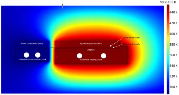
Figure 5.1. Two-thermal-zone microreactor... 103
Figure 5.2. Photograph of assembled microreactor system ... 105
Figure 5.3. Finite element modeling of heat transfer in the reactor setup. ... 106
Figure 5.4. Cross-section of the temperature profile along the reactor ... 107
Figure 5.5. Aminolysis of 22 with 6 in microreactor at 195ºC and 250 psi ... 114
Figure 5.6. Product distributions of aminolysis of SO 5 with 23 ... 116
Figure 5.7. Solvent study of SO 5 aminolysis with 1.2 equiv. of AI 22... 117
Figure 5.8. Production of metoprolol 19 at various amine 17 ratios ... 119
Figure 5.9. Aminolysis to form indacaterol precursor 15 in a microreactor... 121
Figure 5.10. Bisalkylation reaction order determination ... 124
Figure 5.11. Arrhenius correlation of bisalkylation... 125
Figure 5.12. Aminolysis reaction order determination ... 127
Figure 5.13. Arrhenius correlation of SO 5 aminolysis... 128
Figure 5.14. Experimental vs. calculated yields for aminolysis of SO 5 with AI 6. ... 129
Figure 5.15. Modeled yield of 7 with time ... 130
Figure 5.16. Calculated residence time distribution in a tube reactor. ... 133
Figure 5.17. Cartoon of the effect of Dean flow on fluid mixing... 134
Figure 6.1. Experimental microfluidic system for the solids-generating reaction... 141
Figure 6.3. Microchannel clogging by solids agglomeration ... 144
Figure 6.4. Microchannel clogging by wall deposition ... 145
Figure 6.5. Silicon microreactor with a gradual spiral main channel ... 147
Figure 6.6. Wall deposition in a spiral microreactor ... 147
Figure 6.7. Redesigned spiral microreactor with enlarged channels and quench... 148
Figure 6.8. Sequential addition of (a) catalyst and (b) aryl amine... 151
Figure 6.9. Sequential addition reactor design as a circuit diagram. ... 152
Figure 6.10. Sequential addition spiral microreactor... 153
Figure 6.11. Sequential addition spiral microreactor with Rhodamine B... 155
Figure 6.12. Silicon microreactor before and after PTFE surface coating ... 156
Figure 6.13. DRIE fluoropolymer passivation coating in a microchannel. ... 157
Figure 6.14. PTFE-coated microchannel following flow of 20 wt% KOH at 60ºC ... 158
Figure 6.15. Ultrasonication bath waveforms... 160
Figure 6.16. Smoothing of the absolute values of the data in Figure 6.15 ... 161
Figure 6.17. Aluminum chuck for microreactor heating and direct acoustics... 162
Figure 6.18. Ultrasound influence on product yield for different catalyst loadings. ... 164
Figure 6.19. RTD for liquid flow with and without ultrasound... 167
Figure 6.20. RTD for solids-containing flow with and without ultrasound... 167
Figure 6.21. Particle size distribution for Figure 6.18 with and without ultrasound ... 168
Figure 6.22. Pressure drop vs. time for the C-N coupling in the acoustics-irradiated sequential-addition silicon microreactor. ... 169
Figure A.1. Goldilocks reactor mask ...195
Figure A.2. KOH-etched meso-reactor masks...196
Figure A.3. HNA-etched meso-reactor mask. ...197
Figure A.4. First-generation micromixer masks ...200
Figure A.5. Second-generation micromixer masks...201
Figure A.6. Spiral single-addition reactors ...202
List of Tables
Table 5.1. Epoxide aminolyses in a microreactor vs. microwave (μw) batch. ... 113
Table A.1. CORAL Abbreviations ...193
Table A.2. “Goldilocks” KOH-etched reactors ...194
Table A.3. HNA-etched mesoreactor...196
Table A.4. First-generation micromixer ...197
Table A.5. Second-generation micromixer...200
Table A.6. Spiral sequential-addition reactor ...202
List of Schemes
Scheme 3.1. Competing parallel reactions of the Villermaux/Dushman method... 66Scheme 4.1. Formation of NaNT 3 from 5-AT 1 (AT) via DHT 2 intermediate ... 74
Scheme 5.1. General epoxide aminolysis synthesis... 99
Scheme 5.2. Expanded epoxide aminolysis reaction scheme with SO 5 and AI 6... 100
Scheme 5.3. Synthesis of 15 as a precursor to indacaterol 12 ... 101
Scheme 5.4. Synthesis of metoprolol 20 from epoxide 18 and isopropylamine 19... 102
Scheme 5.5. Epoxides and amines used as model substrates. ... 112
Scheme 5.6. Aminolysis of SO 5 with aniline 23; product 30 is often favored... 116
Scheme 6.1. Palladium-catalyzed amination of 4-chloroanisole with aniline... 140
Chapter 1.
Introduction
1.1 Background – Microchemical Systems
The development of silicon microfabrication techniques for the semiconductor industry1 has, in turn, enabled other disciplines to develop microscale devices with a high degree of customizability and precision. Application of mechanical engineering to microscale devices has led to the field of microelectromechanical systems, or MEMS.2 Similarly, the combination of chemical engineering principles, integrated with rapid separation and inline analytical technology, has brought about the development of micro-total analytical systems, or μTAS.3
As a nascent technology, microreactors were developed in the 1990s.3-8 One of the earlier examples of a silicon microreactor system was developed at DuPont as interconnected unit operations.9-11 Since then, a great deal of technological advancement has been made in the field of microfluidic chemical application, both in developing microreactor techniques and in applying them to improved study and processing of chemical syntheses, as recently reviewed by Hartman and Jensen.12
A microreactor, by definition, is a device with functional features that are sub-millimeter in active radius (and often on the order of microns), designed to provide a platform for chemical synthesis. In addition to chemical synthesis, microdevices such as separators, pumps, and flow cells can enable microsystems for multistep synthesis and reaction workup on a continuous scale. A microreactor is typically several centimeters across and is designed for continuous-flow operation through flow channels that are fractions of a millimeter in depth. The reactor volume is most commonly defined by a single long channel up to several meters in length, although parallel-flow reactors with channel manifolds are also used.
The small flow dimensions of the microreactor allow for very low-Reynolds-number, high-Péclet-number flow profiles, making diffusion and dispersion very easy to
characterize and control. In addition, fabricating microreactors out of silicon, which has a high thermal conductivity of 148 W/m·K,13 allows for very fast thermal equilibration and highly precise temperature control. Combined, these features make silicon microreactors unrivaled study tools for reaction screening and kinetics.
In addition to precise reaction control, microreactors have proven to be much safer than large-scale flow and batch vessels. The high ratio of surface area to volume in microreactors provides enhanced heat and mass transfer, useful in such cases as the highly exothermal (-473 kJ/mol) selective direct fluorination of toluene14 and in suppressing flame formation by quenching free-radical generation in hydrogen peroxide synthesis.7
Microreactors have been applied for multiphase reaction acceleration,15 as well as for on-demand synthesis of hazardous intermediates,16 including conversion of chlorine to phosgene.17 Thus, their utility has been demonstrated on the microscale. By developing techniques and methods for rapid and efficient reaction evaluation and kinetic study, microreactor systems can be applied to industrial synthetic schemes and can greatly improve overall process design and development.
1.2 Motivation
In the fine chemical industries, including pharmaceuticals, cosmetics, food additives, agricultural materials, and many other fields, a great deal of time, effort, and cost is dedicated to the development of synthesis processes. Large amounts of reagents and energy are consumed to take a process developed by the chemist in small flasks and to produce a full-scale, multistep, integrated pathway for commercial production. Additionally, many chemical reactions include unstable or difficult-to-isolate intermediates, the production of which is not straightforward to optimize due to their transient nature. Numerous reactions are hazardous to perform, either due to aggressive conditions, toxic reagents, or explosive or flammable intermediates or products. Reducing the scale of such reactions, even in batch, can reduce the hazards to the researcher,18 minimize the time and material consumption for such studies, and provide insight into physical and chemical processes to obtain greater understanding of the systems.
The process of optimizing a reaction can be tedious, expensive, and protracted. In the cases of catalytic reactions, a typical lab may be able to perform only tens of experiments for catalyst and ligand screenings, while an industrial combinatorial chemistry system may be used to run hundreds, if not thousands, of reaction experiments to be performed, each consuming a quantity of typically costly organometallic materials. Once a satisfactory catalyst combination is selected, it is necessary to optimize the reaction conditions to determine a set of parameters such as temperature, stoichiometry, concentration, residence time, etc. at which the most economically beneficial result is obtained. Again, this gamut of parameters can require a large number of experiments. Performing these processes in a microreactor system can greatly increase the efficiency of this process. The ability to manipulate microliter volumes can allow for rapid sequential screenings, consuming only micromole quantities of reagents for each experiment.19 Moreover, the ability to precisely control temperatures and flow profiles ensures that the obtained kinetics are accurate and applicable to a broad range of systems. The ability to perform reactions in flow allows for rapid changes in conditions and reagent proportions with little effort, allowing for a wide range of reaction parameters to be analyzed with a single set of reagent preparations.
Many chemical processes are difficult to perform well by conventional methods such as in batch reactors or in macro-scale flow. Reactions that have long residence times are time-consuming to study and optimize. Syntheses that involve solids cannot be flowed easily, and there are often mass transport limitations that hinder full understanding of the chemistry. Performing chemistries at high temperatures and pressures renders them difficult, and possibly hazardous, to sample during operation. Chemical pathways that require the synthesis of hazardous intermediates are inherently dangerous to operate. The application of microreactor systems can address many of these challenges, providing the ability to safely perform and sample chemistries at a broad range of conditions, to precisely evaluate reaction kinetics, and to safely and efficiently synthesize hazardous intermediates. There is strong industrial interest in continuous processing, both for study and production.20 With a toolbox of microfluidics, many industrial process research and development challenges can be met.
1.3 Thesis Objectives and Outline
To support large research organizations, as well as small academic laboratories, a method of rapidly and inexpensively producing a wide range of silicon microdevices is necessary. Typical fabrication schemes, while highly robust and flexible regarding possible reactor layouts, are limited to a one-wafer-at-a-time etch technique that, in addition to being very time-consuming, is also quite expensive for many research initiatives. To overcome this bottleneck in processing and to reduce the fabrication cost of devices, wet-etch-based alternatives have been developed. Chapter 2 describes the process development and reactor design using two different wet etch techniques to rapidly mass-fabricate batches of silicon reactors.
Many reaction chemistries contain extremely rapid steps, which are often not well understood regarding their kinetics because of mass transfer limitations. For reactions that are highly sensitive to changes in pH or to reagent concentrations, the elimination of concentration gradients at a rate several orders of magnitude faster than the kinetics to be studied is necessary. Additionally, fast mixing remains necessary at large flow scales, as well, requiring a device capable of eliminating concentration gradients without large energy expenditure. To that end, a rapid liquid-flow micromixer with a low pressure drop is designed and developed, as discussed in Chapter 3.
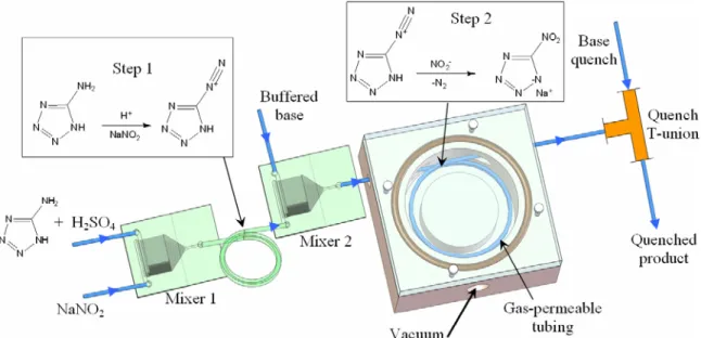
The application of fast microscale mixing to precisely and safely study the kinetics of a rapid reaction with a highly energetic intermediate is demonstrated in Chapter 4. The multi-step synthesis of a nitrotetrazolate compound via a diazonium intermediate in a gas-generating reaction is studied, and the kinetics of both reaction steps are evaluated with accuracy. The synthesis of this energetic compound is too hazardous to characterize through batch experiments; however, using microscale flow chemistry, both the kinetic parameters of each reaction step and the equilibrium of the reactive intermediate are safely determined. Additionally, a slightly modified setup using the same micromixers is applied, based on the determined kinetic parameters, to a scale-up of this reaction, safely generating production-level amounts of the nitrotetrazolate compound with a small lab bench footprint.
To demonstrate the capability of microreactor-enabled conditions to accelerate chemical reactions, Chapter 5 relates the study of β-alcohol formation by epoxide
aminolysis. Through the use of microreactors, the reactions are able to be performed at high pressures, reaching high temperatures in liquid phase while using volatile solvents and reagents. Reactions are shown to be greatly accelerated from their traditional methods, with pharmaceutically relevant compounds synthesized at residence times decreased by a factor of 30-60. A set of model chemistries is explored, providing fundamental understanding of the effects of parameters such as solvent and co-solvent effects and steric hindrance. Additionally, the high utility of the microreactors is demonstrated by enabling a full kinetic study of a multistep mechanism within a short time and with only grams of reagents.
Reactions that produce solids as products or byproducts are highly difficult to perform in flow and thus to efficiently study on the microscale. Chapter 6 describes the use of silicon microreactors to gain fundamental understanding of flow stoppage by solids in microchannels. A palladium-catalyzed C-N coupling reaction between an aryl amine and a substituted aryl halide is used as the model chemistry. Several techniques are evaluated to learn how solid-containing slurries can be made flowable in microchannels. A combination of reactor design and application of acoustic irradiation enabled the flow of the reaction with moderate yield. This has high potential for expanding the microfluidic toolbox to the vast number of chemical syntheses that feature solids, thus allowing them to be studied in microscale systems to attain the aforementioned advantages of reaction acceleration, precise kinetics, and safe, rapid, and efficient reaction study. Finally, Chapter 7 provides some concluding remarks and outlook of future developments in the application of microfluidics to the study of industrially interesting but difficult syntheses.
Chapter 2.
Wet-Etch Fabrication
Silicon microfabrication can be expensive and highly time-consuming. However, for scale-out (parallelization) of silicon fluidic systems, a large number of identical reactors may be necessary for efficient production processes. Similarly, for producing silicon-based full-wafer devices, the ability to simultaneously perform the etching step of the fabrication on multiple wafers would be invaluable for reducing the fabrication cost and time requirement. Acid and base wet-etch techniques were developed and implemented for successful production of silicon micro- and meso-reactors.
A potassium hydroxide etching method was designed to take advantage of silicon crystal properties, producing features etched to multiple depths, including through-holes, in a single etch step. This single-etch-step method was used to produce a set of microreactors possessing channels with both rectangular and triangular cross-sections of multiple depths. Additionally, up to 13 wafers were able to be reliably processed simultaneously.
An HNA (hydrofluoric/nitric/acetic acids) etching method was designed for the production of robust full-wafer mesoscale reactors. HNA can be extremely rapid (600-μm-deep etch in 10 minutes) and etches all crystal planes at equal rates, producing features that are nearly semicircular in cross-section. This process was used to fabricate a mesoscale reactor for reaction scale-up studies, consisting of a single channel 1.25 mm wide and 0.6 mm deep, providing a volume of 5 mL in a compact, easy-to-handle device.
2.1 Silicon Microreactor Etching
At its most basic level, a flow reactor is a sealed vessel (often channel-shaped) with one or more inlets and outlets. Thus, there are several general requirements for the fabrication of any silicon-based fluidic device. One must be able to remove some amount of silicon to create the vessel (channel) shape, to seal said vessel, and to provide fluid access to it, not necessarily in that order. The sealing is typically done by bonding the processed silicon wafer to a capping wafer, either silicon (through fusion bonding)21 or a borosilicate glass (through anodic bonding).22 In either case, the capping wafer can also have been processed, thus having reactor features on both wafers (or even to form 3-dimensional structures from stacks of more than two patterned wafers).23 The fluidic
access can be provided either as part of the reactor features, such as open-ended channels,24, 25 produced in a separate etch step similar to main device etching,15, 26 or micromachined in the capping wafer (in the case of a glass capping wafer, this may be done by laser ablation, ultrasonic drilling, or milling).23 Finally, but possibly most importantly, the reactor features can be etched by a variety of methods, including plasma and wet etch techniques.2
Silicon VLSI (very-large-scale integration) technology allows for a wide range of additional elaborations on this basic design, such as surface modification by oxide growth, chemical vapor deposition, and evaporated metal deposition,27 creating improved chemical resistance properties,28, 29 integrated resistive heaters and thermocouples,30 and bond pads for solder-based fluidic connections.31 However, even with these elaborate components, the silicon etch step to create the channels and the flow ports is often the most costly, at times accounting for the majority of the reactor processing cost.32 This cost, though, strongly depends on the choice of the etching technique, with ones that are the easiest to apply in terms of design flexibility, process automation, and ease of use also being the most costly and time-consuming. The different etching techniques have been reviewed and compared in literature33and in various textbooks on silicon fabrication.1, 2,
27 Each has its advantages and disadvantages; however, to date, there have been no
literature reports of a cheap and efficient technique applied to produce flexible, deep-feature designs in silicon fluidic devices.
2.1.1 Plasma Etching
One of the most preferred methods for creating deep features in silicon is through a plasma etch technique called deep reactive ion etching (DRIE), a variant of reactive ion etching (RIE).2 Plasma etching acts by creating reactive ions that are able to remove exposed silicon atoms into the vapor phase.34 In RIE, the reactive plasma is formed by charged SF6, and the high charge below the substrate causes the ionized gas molecules to
impact the silicon substrate nearly normal to the surface. This leads to a high degree of anisotropy for etches of short duration, although significant undercutting of the mask will occur after prolonged etch times and depths. Thus, this is a very useful method in the semiconductor industry for the fabrication of small steps or vias in the silicon substrate.
To expand the utility of RIE, researchers at Bosch developed the DRIE variant.35 For many chemical species, plasma conditions lead to their polymerization. DRIE takes advantage of that effect by alternating the RIE etching step with one that introduces C4F8
plasma into the chamber. In that step, the substrate charge is reduced; thus, ions are not as strongly drawn downward, and the polymerizing fluorocarbon deposits evenly on all exposed wafer surfaces. When the subsequent plasma etch step occurs, the prevalent downward-directed ions rapidly remove the fluoropolymer layer on the bottoms of the features and continue to etch the silicon substrate, while the side walls are protected from the occasional angled ions. Alternating between the C4F8 passivation and the SF6 etching
allows the etching of arbitrarily deep features with very high aspect ratios. Figure 2.1 shows the etch profiles created by RIE and DRIE.
Figure 2.1. Etch profiles formed by RIE (a) and DRIE (b).
A number of advantages make DRIE highly attractive. First, as mentioned above, it is possible to etch to arbitrary depths with nearly vertical side walls. This feature allows for the production of a wide variety of designs, as any two-dimensional feature or drawing will be extruded vertically into the depth of the silicon wafer. Device design thus becomes limited only by the resolution of lithography in the masking layer. The
Silicon Photoresist
second advantage is a relatively high selectivity of the etchant for silicon over certain photoresists (40:1 etch rate ratios), allowing for a simple and relatively inexpensive method of producing mask layers and defining features. Similarly, DRIE has a high selectivity for silicon over thermal silicon oxide (100:1 etch rate ratio), making the frequently used thin layers of thermal oxide a good functional mask for DRIE, especially if nested mask use is desired. Finally, the high degree of control that modern DRIE equipment allows over the gas composition, plasma power, chamber pressure, and process timing allows for tailoring of etch methods for different applications, as well as a high degree of reproducibility for the same method.
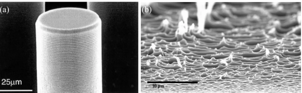
On the other hand, there are several disadvantages to DRIE that may lead one to consider other etching methods. First, because DRIE is in fact not truly anisotropic, but is rather a series of slightly isotropic etches interspersed with passivation steps, the side walls are not smooth. Instead, they are scalloped, as shown in Figure 2.2a, creating micron-level surface texture. Additionally, the etch creates a high degree of sub-micron surface roughness due to the incident ion bombardment. Therefore, without an additional HNA polishing step (see section 2.1.3 for more details), the process results in sub-microscopically rough side walls, as shown in the scanning electron microscopy image of Figure 2.2b. Second, to produce through-holes, additional steps are necessary to mount the substrate wafer onto a handle to prevent the helium coolant flow from leaking into the vacuum chamber, thus requiring additional processing time.
Figure 2.2. Scanning electron microscopy images of DRIE-etched side wall, showing (a) scalloping36
and (b) surface roughness.
With DRIE, the etch depth uniformity across the wafer surface is strongly dependent on the etch parameters, with there being a trade-off between etch rate, selectivity,
anisotropy, and uniformity.37 The etch recipes must select a middle ground to have reasonable values for all of these properties. Thus, the methods preferred by users experienced on the particular piece of DRIE equipment available to us typically have high anisotropy and etch selectivity, a reasonable etch rate of 1 to 2 μm/min, and a depth variation of approx. 10% from wafer center to wafer edge. This is a significant difference that often requires reactor designs, layouts, and arrangements on the wafer to have depth-insensitive features (such as through-holes or halo etches) nearer to the edge of the wafer to allow more control over the depth of more sensitive features. Additionally, the aforementioned etch rate means that for thicker wafers of 1000 μm that require through-holes, it is not uncommon to require 12 to 15 hours of combined etch time per wafer. When combined with the fact that DRIE can only be performed on a single wafer at a time, it is easy to see how the etch step can become a significant bottleneck when it is necessary to process several wafers, especially if full-wafer devices or a multi-wafer stack are desired.
DRIE requires a high degree of technology to control the process;38 combined with the cost of the reactive gas and the high energy expenditure over very long periods of time, this makes DRIE one of the most expensive microfabrication processes per wafer32 when deep features and/or through-holes are required by the process. All of the discussed shortcomings are the reason for developing alternative etch processes to be inexpensive, robust, and reproducible.
2.1.2 Potassium Hydroxide Etching
There are several well-known wet etch methods for silicon. Methods that use caustic aqueous solutions, such as potassium hydroxide (KOH) and tetramethylammonium hydroxide (TMAH), the two most widely used etchants, act via the hydroxide ions, which are thought to react with silicon to form silicon hydroxide anions, as well as hydrogen gas. Caustic wet etches have high selectivities towards certain crystal planes, with etch rate ratios of as high as 100:1 for {100} vs. {111} crystal planes.39 This crystal plane selectivity lets certain planes act as etch stops, resulting in constrained, regular features.
Although an aqueous solution of KOH can be used as the etchant to anisotropically etch vertical features in (110)-oriented silicon wafers,40 such wafers are typically very
expensive; thus, (100)-oriented wafers were our substrate of choice. Applying KOH to (100)-oriented silicon wafers (respectively, the most commonly available, and thus the least costly, etchant and silicon wafers), the etch stop planes are at a 54.74º angle to the surface.41 Thus, any feature, if etched sufficiently deeply, will form either a pyramidal or a triangular-prism pit bounded by {111} crystal planes (Figure 2.3). This feature can be both an advantage and a hindrance. It is advantageous because it ensures that all etched features are aligned to crystal planes, which is necessary for devices such as waveguides23 and optics.42, 43 However, it also means that any feature that is misaligned from the crystal plane in lithography will etch out larger than is designed, as the bounding etch planes will be slightly outside the feature bounds.
Figure 2.3. Illustrations of features etched by KOH: side view (a) and top view (b); the dashed line represents the cut along which the side view is made.
For the etching procedure of aqueous KOH on (100)-oriented silicon wafers, design of features is highly important, especially for fluidic devices such as microreactors. Nearly all features to be etched by KOH are designed to be rectangular and aligned along the <110> direction. These features form either pyramidal pits or long straight channels with triangular or trapezoidal cross-sections. These have been used in the past for parallel-channel reactors23 and fiber alignment channels.31 However, knowing the etch rates of the crystal planes, it has been possible to develop methods to compensate for convex corner etching.44-46 These methods have been used to create series of channels that take 90º turns (always aligned along the <110> direction), thus expanding the possible length of the fluidic channels that can be used for microreactors.
There are several caveats, however, to using these corner compensation methods. First, the corner compensation features must be calculated for a specific etch depth. Therefore, each design and mask is only usable for reactors of one depth. A related issue is that the desired etch depth determines the size of the corner compensation features.
Silicon Nitride
Thus, deeper etches require larger corner compensation features, limiting how closely spaced adjacent channels can be placed and increasing unutilized silicon area. If multiple features with convex corners are desired to have different depths, then the all of the corner compensation features must be sized to the maximum desired depth. Otherwise, the shallower features will have the convex corners be etched inward and deeper due to the unavailability of the etch-terminating planes (this, however, may be acceptable for certain features such as low-volume mixing zones).
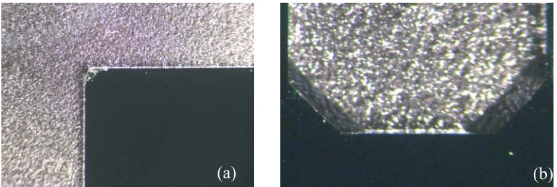
Figure 2.4. Illustration of side view (a) and top view (b) of a 90º turn aligned to <100> direction; the dashed line represents the cut along which the side view is made.
Figure 2.5. Photographs of the inside corner of a 90º turn and the outside corners of a 180º turn with KOH etching (the etched area is silver-grey, and the unetched area is dark-green).
Another method of etching channel-type features with KOH in (100) wafers is by aligning the long rectangular features along the <100> direction.47 This places the etch-terminating {111} planes 45º to the feature sides, and the fast-etching {100} planes are now parallel to the features. As a result, the feature etches both downward and laterally, undercutting the mask along the long sides of the rectangular feature at the same rate as the vertical etch (Figure 2.4). In the process, channels with perfectly vertical walls and a sharply delineated rectangular cross-section are formed along most of the feature. At the short sides of the rectangle features, the channel is bounded by the {111} planes aligned 45º to the original feature – the <110> direction – at the feature corners, sloping into the
Silicon
Nitride
(a) (b)
etch at a 54.74º angle. Thus, if two long rectangular channels are joined at a 90º angle, the turn would have a perfectly sharp 90º corner with vertical side walls on the inside turn, and two vertical walls connected by a 54.74º-sloping wall at two 135º angles on the outside turn (Figure 2.5).
Using the method of channel alignment to the <100> direction can be very useful, as channels can now be placed arbitrarily close to each other, providing better utilization of silicon area. It is important that lithographic features to produce these channels be designed accounting for the lateral etch, the rate of which will now be equal to the vertical etch. Another major advantage is that this method produces rectangular channels, which have significantly less pressure drop for the same volume at the same etch depth. Additionally, the rectangular cross-section is more familiar to those experienced with DRIE or bulk machining for microreactor production.
KOH etching has several advantages over processes such as DRIE. One such advantage of this process is the highly smooth walls formed by the crystalline etch. Secondly, features with multiple depths can be achieved in a single etch step. By aligning certain features along the <110> direction and allowing them to self-terminate while having other features aligned along the <100> direction, it is possible, for example, to create a reactor with relatively deep channels with rectangular cross-sections, with shallow triangular channels for a mixing zone, with less shallow triangular channels for a quench mixer, and having very shallow alignment marks on the wafer (here, the shallowness is desirable to reduce undue stress on the wafer from unnecessary etches). Considerations must be made, though, for corner compensation limitations for the triangular channels with large depth disparity. Additionally, because the wafer would be exposed to the KOH solution equally on both sides, it is possible to simultaneously etch features on both sides of the wafer. Thus, through-hole ports and, for example, channels for heat exchanger fluid can be placed on the back side at the same time. This also reduces the necessary etch time as compared to DRIE. At typical process conditions, the etch rate of the KOH process is similar to that DRIE, 1 to 2 μm/min. However, because through-holes are etched at the same time, a process requiring 700-μm-deep channels with ports in a 1000-μm-thick wafer requires only 70% of the etch time of DRIE for the same features.
A predominant advantage of KOH etching is its high uniformity. The KOH etch is kinetics-limited and not limited by diffusion. With a sufficiently good temperature bath to ensure no thermal gradients across the wafer and wafer-to-wafer (a fairly easy task), the etch difference across the wafer and between wafers is often as low as 1%. As many as 25 wafers can be easily placed in a single wafer boat and etch container. Thus, 2 sides each of 25 wafers can be uniformly processed with a single etch step, or 50 times the throughput of DRIE. Combined with the extremely low cost of KOH, the low energy expenditure, and the low level of technology required for this process, this renders KOH etching a far cheaper alternative to DRIE.
There are several disadvantages to using KOH, as well. First, there is far less flexibility in reactor design as compared to DRIE. Because one is limited by the crystal planes, features must be aligned along the <110> or <100> directions on the wafer, and only 45º and 90º turns can be formed, with no possibility for curvature. Moreover, the features aligned in the <100> direction will always have a width of twice the depth plus the lithographic feature width. Thus, the minimum aspect ratio of those features can only approach (but never reach) 2. Second, the mask for the etch must be either silicon oxide (suitable for relatively shallow etches) or silicon nitride (necessary for deeper etches). Both cases require additional processing steps, and for silicon nitride, not an insignificant additional cost. However, the etch rate of silicon nitride in KOH is very low, and a 0.2-μm film of nitride is sufficient for a 750-0.2-μm-deep etch. Additionally, up to 50 wafers can be processed at once for silicon nitride deposition. Thus, a thin layer of nitride and a large batch size can make the cost per wafer very low.
Another disadvantage of KOH is the high sensitivity of the etch to the quality of the lithography, especially for features aligned in the <100> direction, where the lithographic features are much finer than the desired etched ones to account for the lateral etch. In those cases, very fine breaks in the feature would cause channel terminuses because they would be immediately bounded by etch-stop planes. Similarly, slight enlargements of the features may cause breaks in channel walls due to the lateral etch if thin walls are desired (see section 2.3.1 for discussion and illustrations). With <100>-aligned features, etch stops such as a buried oxide layer would not stop the lateral etch, reducing the utility of that method. Finally, because the etches are along crystal planes, especially for channels
with rectangular cross-sections, there are high stress concentrations along the etched corners, lying directly on crystal planes, thus making KOH-etched wafers much more fragile and resulting reactors less robust to stress (see section 2.3.3 for discussion and illustrations). However, a brief HNA etch step following the KOH process can smoothen the crystal corners and disperse the stress accumulation.
2.1.3 Acidic Wet Etching
In addition to the caustic wet etching methods described in the previous subsection, acidic wet etch methods also exist. The best-known such method is one that uses a mixture of hydrofluoric, nitric, and acetic acids (HNA).48 This etch solution has been well characterized in terms of the silicon etch rates in mixtures with varying proportions of the three components.49 The nitric acid component is a strong oxidant, capable of
acting on silicon to form silicon oxide. The second active component, hydrofluoric acid, is an etchant of silicon oxide; thus, in HNA, it removes the SiO2 formed by nitric acid
oxidation, exposing more bare silicon. Between the two acids, silicon becomes etched isotropically, forming quarter-circular undercuts under the exposed feature edges. The purpose of acetic acid in the mixture is only as a dilutant; while water can be used, it also changes the dissociations of HF andHNO3, thus making an acid preferable for this
purpose. A diluent is necessary to be able to control this process, which is otherwise extremely rapid and highly exothermal.
As briefly mentioned above, HNA is commonly used for various polishing and crystal plane stress removal purposes. Because it is a fully isotropic process (assuming sufficient mass transfer), etching occurs fastest around the greatest surface area; thus, corners formed by KOH and micron-scale ridges, bumps, and protrusions that are a product of DRIE can be quickly removed by fairly mild HNA. However, HNA is a highly aggressive etchant, and no masking technique is very resilient to it. For that reason, to the best of my knowledge, it has not been used for deep features.
The strongly oxidative property of nitric acid makes the selection of a mask for deep etching rather difficult. Organic masking layers such as photoresist are removed by HNA in a matter of seconds. Similarly, most metals are rapidly oxidized by nitric acid, not to mention the large cost associated with metal deposition. It is physically feasible to use
electron-beam evaporation to deposit a thin layer of gold atop an adhesion layer of titanium, as gold would easily withstand HNA; however, the titanium oxide/silicon oxide forming the true adhesion layer will likely succumb to the etchant after a short period. Additionally, the cost of the metals and the use of equipment, combined with the small number of wafers capable of being processed simultaneously (4 on the machine available to us) make this application prohibitively expensive. As hydrofluoric acid etches silicon oxide, that material is not usable as a masking layer.
The material typically used as a mask for HNA is silicon nitride deposited by low-pressure chemical vapor deposition (LP-CVD). It has excellent adhesion properties to silicon, without peeling even at the most aggressive conditions. Additionally, it is fairly resilient to HNA, with HNA selectivity toward silicon versus silicon nitride of as high as 600:1, depending on the temperature and HNA composition. However, it is impractical to deposit silicon nitride with large thicknesses; 2 μm is the maximum deposition thickness in a single coating layer. This is not a major limitation because, if an appropriate composition of HNA is used, this is sufficient to allow etching down to 650-700 μm, producing quite deep features for large fluidic devices. Moreover, silicon nitride deposition can be a moderately expensive process per batch,32 although this is moderated by the ability to coat up to 50 wafers in a single batch.
As with any other technique, HNA offers a number of advantages and possesses several disadvantages as compared to KOH and DRIE. Being a wet-etch technique similar to KOH, HNA enables the simultaneous etching of multiple wafers in a single batch. It also allows simultaneous etching of features on both sides of the wafer; however, with HNA, it is not possible to design an etch stop. Thus, two-sided processing can be used to produce through-holes or to create sets of features that are both less than half of the wafer thickness; it is not possible to etch to multiple depths in a single step.
HNA produces features that are rounded in cross-section. With sufficiently fine lithographic features, the cross-sections of channels would be nearly semicircular, although this depends on the mass transfer (Figure 2.6). This may be advantageous for applications requiring lower dispersion, especially multiphase liquid or gas-liquid flows, where having two corners instead of four would reduce the dispersal of the wetted phase under proper flow conditions. Additionally, such a wafer can be fusion-bonded to one
that has a mirror-image pattern, forming a sealed silicon channel with a nearly circular cross-section and thus reproducing the familiar polymer or steel tube, but with the advantageous properties of silicon and with far more freedom of reactor layout. Although, similarly to KOH, any HNA-etched feature would have an aspect ratio of greater than 2, the lack of crystal plane limitation significantly expands the flexibility of reactor design, allowing for arbitrary shapes such as winds, serpentines, and spirals. Moreover, because the etch is not along any crystal planes and because no sharp corners are formed within the silicon, there are no places of high stress accumulation. In addition, the rounded features ensure that the force of the pressure from the liquid is normal to the bulk of the silicon and is dispersed in all directions and not focused on any one plane. Thus, the HNA-etched reactors are expected to be the most robust to pressures and stresses for the same feature sizes and layouts.
Figure 2.6. Illustrations of HNA-etch profiles with (a) and without (b) agitation.33
Another feature of HNA etching is its extremely fast etch rate under certain compositions, which is both an advantage and a hindrance. Because HNA etch is exothermal, it can also be difficult to control at the faster etch rates due to the inability to sufficiently rapidly remove heat. At slower etch rate compositions, however, the selectivity toward silicon over nitride also significantly decreases. Nonetheless, at the composition found to be optimal for both etch rate and selectivity (see section 2.3.3 for a detailed discussion), the etch rate of silicon was 100 μm/min, or 50-100 times faster than either KOH or DRIE. The fast etch rate, however, makes this etch somewhat mass-transfer-limited. Thus, a very good mixing strategy is necessary to ensure uniform etching across the wafer and wafer-to-wafer. An etch difference of ~10% was typically found between the center and the edge of the wafer; however, this being an isotropic etch, this causes a cross-sectional area difference of ~20%, making an etch rate difference similar to that with DRIE create a much more significant channel volume difference.
Silicon
Nitride
The fast etch rate makes this process ideal for fabrication of large devices such as full-wafer fluidic reactors, where one wants to process many wafers at once. Even without the availability of good mixing to ensure good wafer-to-wafer uniformity within the tank, a magnetic stirrer is sufficient to provide acceptable across-wafer uniformity. With a fast etch process, it is easy to rapidly process many wafers sequentially using only a small amount of material, making this a highly economical process.
2.2 Reactor Design and Fabrication
Fluidic reactors were designed with consideration for the most efficient fabrication route within the constraints of the available microfabrication facility. Additionally, it was desirable to maximize the utility of the silicon surface; i.e., the designs were made to produce the maximum total reactor volume from a single silicon wafer. A design was made for a set of microreactors to utilize the etch-controlling advantages of KOH etching. To produce mesoscale reactors, separate designs were made for both KOH and HNA etching techniques. In both cases, single processed silicon wafers were capped with clear borosilicate wafers to retain visual access to fluid flow and possible reactor fail modes.
2.2.1 KOH-Etched Reactors
Microreactor Design
To take advantage of the ability to etch multiple depths in a single etch using KOH wet etch processing, it was decided to design a set of reactors that will have shallow, self-terminated channels for rapid mixing of incoming reagents, deep rectangular channels for the main residence time and for the quench, and through-hole ports for reagent and quench inlets and the outlet, as well as deposited metal pads for solder-based packaging.
The most frequently used silicon wafer thickness for microreactor fabrication has been 650 μm; thus, this was the thickness selected for these reactors, as well. It was decided to mimic the layout of previously designed and widely used DRIE-etched microreactors15, 19, 31 regarding reactor layout, port positioning, and main channel depth. It was decided to use only two inlets, as that is the most commonly used configuration. If more inlet streams are required, it is possible to use a union upstream of the inlets or, if
rapid mixing is necessary, a micromixer (for more on those, see Chapter 3). Based on prior simulations that best quenching occurs using a large volume of quench flow, the channel following the inlet quench was designed to be quite large, 1.5-mm-wide, to accommodate such diluent flows.
Based on the aforementioned DRIE design, the channels were designed to be 400-μm deep, which satisfied the constraint that they be more than half the thickness of the wafer to allow the simultaneous etch of through-holes. Combined with the lithographical feature size, the selected depth also set the channel width, as the alignment to produce vertical side walls also etches silicon in the lateral direction. Based on the quality of the high-resolution transparency printer (Pageworks, Cambridge, MA), channel lithographic features of 50-μm width were printed. Thus, the reaction channel were 850 μm in width (400-μm etch in each direction plus 50 μm of the printed feature). The channel turns were designed to be even wider (average turn radius of 1.25 mm) to allow reactions with small amounts of precipitate to maintain flow, as it was previously observed that precipitates tend to agglomerate and clog around turns. Channels were spaced so as to allow 100 μm of wall width between them, resulting in a dense channel packing and high silicon utilization.
For the mixing zone, the channels were aligned along the <110> direction to self-terminate, thus forming shallow channels with a triangular cross-section. Because the channels had 90º turns, corner compensation was necessary to reduce overetching of the convex corners (Figure 2.7). However, as the main etch depth was significantly greater than that of the mixing zone, sizable corner overetching was expected to occur regardless of the compensation features. This was acceptable for the mixing zone, as it reduced the pressure drop in that section without significantly affecting mixing effectiveness.
Figure 2.8 shows a comparison of the mask features, intended etched reactor, and an actual photographed reactor. The black region on the diagram indicates the printed mask features, whereas the blue region indicates the intended etched reactor area (not including the convex corner overetch). The orange circles represent the bonding pads of deposited metal, which would appear on the back side of the reactor. It can be seen that the fabricated reactor matches the design very well, although, as the expanded section shows,
the corner compensations are insufficient for such a disparity between mixing channel depth and maximum depth.
Figure 2.7. Corner compensation features; the white area represents unetched silicon, black shading represents the mask design, and blue shading represents the intended etched feature; channel width is 200 μm, and the finest feature size is 10 μm.
(a) (b)
Figure 2.8. KOH-etched microreactor: (a) illustration of the mask (black) and the desired etched features (blue), with bonding metal pads on the back side (orange); (b) photograph of reactor.
Different reaction chemistries may demand different residence times, and because certain sample volumes are required for analysis, slower reactions often require larger reactor volumes so as to be able to produce sufficient quantities within a reasonable time. To that end, three different microreactors were designed for different flow rate ranges, allowing future users to select from among small (92 μL), medium (200 μL), or large
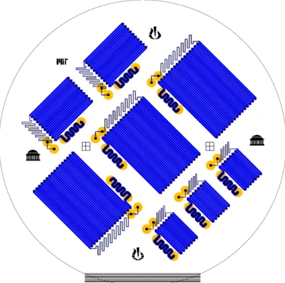
(460 μL) reactors, henceforth referred to as the Goldilocks set. The volume was generated by the number and length of the channels, keeping the same depth and width, thus simulating a user selecting different total lengths of tubing of the same type. Figure shows the wafer layout with the three designs.
Figure 2.9. Illustration of the layout of the Goldilocks devices on a wafer.
The different reactor designs had different areas for the mixing channels. However, with simple single-channel laminar mixers, there is a trade-off between pressure drop and mixing time. Smaller-width channels are desirable for their ability to effect mixing more rapidly, as the characteristic mixing time is dictated by the diffusion distance, as follows:
2 2 x t D = 2.1
where D is the diffusivity and x is the mixing distance. In the case of triangular channels and two incoming streams, x is the equivalent diameter, determined by solving the Navier-Stokes equation for a Newtonian fluid in an isosceles triangle channel. Longer channels also provide more time for mixing at a given flow rate.
Both smaller and longer channels, however, result in greater pressure drop. For laminar flow through channels, the Hagen-Poiseuille equation dictates the pressure drop, which is once again dependent on the equivalent radius of the channel. For isosceles triangles, the Navier-Stokes equation has been solved to give the equivalent radius as a function of the triangle base (channel width) and angle.50 Thus, for KOH-etched channels with 54.74º angles, the Hagen-Poiseuille equation can be reduced to the following: 4 278Q L P w μ Δ = 2.2
where ΔP is the pressure drop, Q is the flow rate, μ is the fluid viscosity, L is the channel length, and w is the maximal (top) width. Thus, it is obvious that pressure drop and mixing both depend linearly on channel length; however, while mixing time decreases with the square of channel width, pressure drop increases with the fourth power of channel width. Therefore, one should maximize the channel width where possible to prevent an unreasonable pressure drop.
As the smallest reactor was the most constrained in terms of area, it was used as the basis of the mixing zone design. Based on the reactor volumes and on previous experience with chemistry in microscale flow, total reagent flow rates on the order of tens of microliters per minute were considered typical. Thus, the mixing zone was designed to provide three times the characteristic mixing time (fully diffused flow to three standard deviations) at a flow rate of 30 μm/min. The <110>-aligned channels must be spaced apart at a distance of at least twice the channel width to allow for corner compensation; otherwise, corner overetch would significantly reduce the mixing channel effectiveness. With the channel width constraining how many channels can be packed in a given area, thus limiting the total length of the zone, the maximum width to still allow the minimum desired mixing was determined at 200 μm. This results in a very tolerable pressure drop of 5×10⁻² bar at 30 μL/min flow of water.
For the larger reactors, the mixing zones were resized to fit within the larger available areas. As the larger reactors were made so to allow for longer residence times at similar flow rates, the upper bound of 30 μL/min was maintained. The mixing zones were then enlarged so as to continue providing three characteristic mixing times at this flow rate,
but with a minimal pressure drop. For the medium and large reactors, the mixing channel widths were 250 and 300 μm, respectively, with channels being spaced farther apart than twice the channel width. In both cases, the pressure drops were significantly smaller. Additionally, the greater distance between the channels allowed for larger corner compensation features. Combined with the larger mixing channel depth (and therefore a smaller difference between the mixing and reaction channels), this would produce much smaller corner overetching (see section 2.3.1 for the results).
Mesoscale reactor design
For scale-up of silicon fluidic systems, it is appropriate to investigate scaling effects in silicon mesoscale devices. Such devices would afford the advantages of silicon reactors, such as robustness to high temperatures and pressures, very fast thermal equilibration, reduction of hot spots due to silicon’s high thermal conductivity, and the ability too observe the reaction in progress, which is invaluable when studying multiphase or solids-generating reactions, especially with regard to scaling studies.
10.5 cm 10.5 cm
1.55 mm x 0.75 mm channels
Figure 2.10. KOH-etched meso-reactor: (a) illustration of the desired etched features; (b) photograph of reactor.
The KOH-etching technique was applied to maximize the possible volume etched out of a silicon wafer. To that end, a 1000-μm-thick wafer was used as the substrate for the design. It was decided to produce a single channel, with any other functions (mixing,
quench, etc.) to be performed up- or downstream of the device. For ease of handling, the reactor was to be rectangular, and as wafer handling during fabrication proscribes placement of features closer than 1 cm to wafer edge, the design was to be a square inscribed in a 13-cm-diameter circle.
The channel depth was selected to be 725 μm, thus resulting in channel width of 1.5 mm, as discussed for the microreactor design. This allowed 57 channels of 9-cm length to be packed next to each other, with 100-μm separation, resulting in a 5-mL reactor, an order of magnitude larger than the largest Goldilocks device. Figure 2.10 compares the intended reactor layout and an actual device.
Fabrication method and techniques
The detailed process run sheet for the KOH etching process is given in Appendix A. In brief, the procedure for the fabrication consisted of mask layer deposition, lithography, etching, protective layer growth or deposition, and bonding.
To serve as a mask layer, 200 nm of LP-CVD silicon nitride was deposited on the surface of virgin silicon-(100) wafers (Silicon Quest International, Inc., Santa Clara, CA) with flats cut along the <110> direction. Photolithography was performed using 1 μm of thin photoresist (OCG 825 positive resist), following the standard operating procedure (SOP) using an Electronic Visions EV620 Mask Aligner. It is critical during the UV exposure to align the photomask to the crystal plane of the wafer. As can be seen in Figure 2.9, the mask has a number of closely spaced horizontal slits at the region of the wafer flat. By looking through those slits on the mask, it is possible to view and align the wafer.
For wafers containing features on both sides, the two lithography steps were performed sequentially prior to nitride etching. To do so, photoresist coated on one side of the wafer was pre-baked (Blue M Model DDC-146C oven, 95ºC) for only half of the time prescribed by the SOP (15 minutes instead of 30), followed by coating of the other side and a full pre-bake time. It is best to first coat the side with more critical features (i.e., channels), as opposed to the side with features such as ports.
After exposure of the front side, the wafers were developed for 20% of the SOP-prescribed development time (12 seconds out of 60, in OCG 934 1:1 developer),
sufficient to make visible the features, including alignment marks. After exposure of the second side, development was performed until all features appeared fully developed when viewed under the fluoroscope. Following development but prior to post-baking, the edges of the wafers were “painted” with photoresist using swabs to protect the nitride at the rim. This prevents the rim of the wafer from being etched in KOH, which would result in a jagged edge, making the wafers more brittle and difficult to handle. Optimally, wafers would be developed as a batch, using a Teflon cassette to submerge them. However, if it was desired to develop one wafer at a time, care was made to ensure flow of developer to both sides of the wafer (i.e., the wafer was not permitted to lie flat on the bottom of the developer dish).
When performing two-sided lithography, great care must be taken not to inadvertently scratch or damage the resist on either side, as this would result in flaws during etching. Alternatively, it is possible to perform lithography and nitride etching on one wafer side at a time. This requires more processing time, although it is easier to handle wafers that only have process-critical resist on one side.
The nitride mask layer was etched using RIE (Lam Research Model 490B Reactive Ion Etch), following an SOP. After removal of the photoresist (piranha solution, 10 minutes), the wafers were placed into a 25 wt% KOH solution (aqueous) at 80ºC. This resulted in etch rates of approx. 60 μm/hr, varying slightly based on the silicon doping, resistivity, and possible deviations on bath temperature. After 1 hr of etch time, the wafers were removed, and features were measured to more precisely determine the etch rate and calculate the etch time. Measurement was done under an optical microscope, comparing the depths of the top and bottom of a vertical side wall, doing so at several places on the wafer. One hour prior to calculated etch end, this was repeated, and the final etch time was determined. When wafers from multiple processes were etched simultaneously, the final-hour etch measurement was performed for each process’s wafers, and as the less deeply etched wafers were completed, they were removed, allowing other ones to be etched further. In this fashion, several processes’ wafers could be etched at the cost of a single etch step.
To ensure uniform etching with smooth channel side walls and bottoms, wafers were oriented vertically within the bath. This allowed the large amounts of evolved hydrogen