Contact-Printed Microelectromechanical Systems
byApoorva Murarka
B.Sc., Electrical Engineering, Massachusetts Institute of Technology (2010)
Submitted to the Department of Electrical Engineering and Computer Science in partial fulfillment of the requirements for the degree of
Master of Engineering in Electrical Engineering and Computer Science at the
MASSACHUSETTS INSTITUTE OF TECHNOLOGY June 2012
@
Massachusetts Institute of Technology 2012. All rights reserved.Author ... ... ...
Department of Electrical Engineering and Computer Science
May 25, 2012
Certified by ... U ....
Vladimir Bulovid
Professor of El trical Engineering and Computer Science Thesis Supervisor
A ccep ted by ... ... ... -
-Professor Dennis M. Freeman Chairman, Masters of Engineering Thesis Committee
Contact-Printed Microelectromechanical Systems
by
Apoorva Murarka
Submitted to the Department of Electrical Engineering and Computer Science on
May 29, 2012
in partial fulfillment of the requirements for the degree of Master of Engineering in Electrical Engineering and Computer Science
ABSTRACT
Microelectromechanical systems (MEMS) are ubiquitous. Scalable large-area ar-rays of MEMS on a variety of substrates, including flexible substrates, have many potential applications. Novel methods for additive fabrication of thin (125±15 nm thick) suspended gold membranes on a variety of rigid and flexible cavity-patterned substrates for MEMS applications are reported. The deflection of these membranes, suspended over cavities in a dielectric layer atop a conducting elec-trode, can be used to produce sounds or monitor pressure. The reported fab-rication methods employ contact-printing, and avoid fabfab-rication of MEMS di-aphragms via wet or deep reactive-ion etching, which in turn removes the need for etch-stops and wafer bonding. Elevated temperature processing is also avoided to enable MEMS fabrication on flexible polymeric substrates. Thin films up to
12.5 mm2 in area are fabricated. The MEMS devices are electrically actuated and the resulting membrane deflection is characterized using optical interferometry. Preliminary sound production is demonstrated, and further applications of this technology are discussed.
Thesis Supervisor: Vladimir Bulovid
Acknowledgments
First, I would like to thank my advisor, Professor Vladimir Bulovid. His advice,
support, patience, humor, and encouragement over the past four years have been invaluable. I would also like to thank him for providing me with the opportunity and the resources to carry out the research that I love so much. Additionally, I am grateful for his willingness to entertain some of the crazier ideas involving my research from time to time. I look forward to growing as a researcher under his mentorship during my forthcoming Ph.D. years.
Next, I would like to thank Professor Jeffrey Lang for all of the valuable time he has spent on countless technical discussions concerning my research and its potential applications. His enthusiasm for this project has constantly fueled its progress. A great deal of the analysis performed in this thesis is a direct result of his intense guidance and assistance. Additionally, I am greatly indebted to him for helping me with countless revisions of my papers, posters, and presentations. I look forward to further evolving my approach to engineering problems under his guidance during my Ph.D. years.
I would also like to thank current and former members of the Organic and
Nanostructured Electronics Lab for making research and work so enjoyable. Spe-cial shout outs to Annie, Farnaz, Joel, Yasu, Tim, Trisha, Wendi, Geoffrey, Jill, Andrea, Costi, and Eletha. Patrick-thank you for being such a great friend and a colleague. Special thanks go out to Corinne Packard, Vanessa Wood, Matt Panzer, Alexi Arango, Scott Bradley, and Sarah Paydavosi for showing me the ropes in lab when I was a UROP.
Special thanks go out to Ms. Anne Hunter, Ms. Linda Sullivan, and Ms. Vera Sayzew for all of the help and advice given during my undergraduate and M.Eng. years at MIT, and for ensuring that I graduated on time!
Additionally, I would like to thank all of my friends, and in particular Amey, Chintan, Adam, and Sagar, for all of the support, the discussions, and the fun!
Special thanks also go out to Mr. Ravi Meattle-his confidence in my abilities is reassuring.
Finally, I would like to thank my father and my late mother for their support and advice. They have had a great impact in shaping me while giving me the freedom to develop my own interests.
Contents
1 Microelectromechanical Systems
1.1 Microcontact Printing of MEMS . . . . 1.2 Prior Work and State of the Art . . . .
2 Modeling of PDMS Spacer Layer Pressure Sensors
3 MEMS Fabrication on PDMS Spacer Layers
3.1 Photolithography Transparency Masks ...
3.2 SU-8 Master Molds . . . .
3.3 Pick-up Stamp Substrates . . . . 3.4 Transfer Pad with Raised Mesas . . . .
3.5 Contact Lift-Off Transfer . . . . 4 PDMS Spacer Layer Device Characterization
5 Contact-Transfer Printed MEMS Membranes on Silicon Dioxide 5.1 Prior Work and State of the Art . . . .
5.2 The Acetone-Assisted Contact-Transfer MEMS Fabrication Process
5.2.1 D evice Design . . . .
5.2.2 Pick-up Stamp Substrates . . . .
23 25 26 31 39 39 40 41 42 43 47 53 54 55 56 57
. . . .
. . . .
. . . .
. . . .
. . . .
5.2.3 Transfer Pad with Raised Mesas . . . . 5.2.4 Contact Lift-Off Transfer . . . .
6 Silicon Dioxide Spacer Layer Device Characterization
6.1 A nalysis . . . . 6.1.1 Determining Young's Modulus . . . . 6.1.2 Potential Sound Pressure Level Output . . . .
7 Quality of Contact-Printed Films on Silicon-based Substrates 7.1 Surface Roughness of Transferred Gold Films . . . . 7.2 Defects in Gold Films Transferred onto Cavity-Patterned Substrates
7.2.1 Irreversible Stiction of Gold Films to Cavity Sidewalls and Cavity Bottom . . . .. 7.2.2 Excessive Stretching of Gold Membranes over Cavities
8 A Prelude to Contact-Printed Acoustics
8.1 Sound Production . . . .
9 Avenues for Further Research
9.1 Device Geometry . . . . 9.2 Transfer of Films of Different Metals and Graphene . . . . 9.3 Stamping Apparatus . . . . 9.4 Fabrication on Substrates with Patterned ITO-Electrodes . 9.5 Phased Arrays of Sound Sources and Beam Steering . . . 9.6 Demonstration as Microphones . . . . 9.7 Manipulation of Light Incident on a Surface . . . .
58 59 63 68 68 70 73 73
77
77
82 87 91 95 . . . . 95 . . . . 96 . . . . 97 . . . . 97 . . . . 98 . . . . 99 . . . . 100List of Figures
1.1 An overview of the microcontact printing process. The stamp consists of a PDMS layer that has been patterned with ridges that are about 25 Lm wide, with 25 im spacings between the ridges. The transfer pad consists of a viscoelastic substrate, such as PDMS, coated with an organic release layer, upon which a thin film of metal has been evaporated. The stamp is brought into contact with the metal film on the transfer pad, and it is rapidly peeled away, picking lip the metal film from the transfer pad. The metal film bridges the gaps across the ridges in the PDMS if the stamp is peeled away from the donor transfer pad fast enough. The diagram above is not drawn to scale. . . . . 26
1.2 Process flow for contact lift-off transfer, as demonstrated by Packard, Murarka, et al. The last picture in the process flow shows that the PDMS ridges on the stamp are bridged by the lifted-off gold membrane, with air gaps between the ridges and beneath the membrane. The resulting
MEMS variable capacitor can be used as a component of a variety of
1.3 Capacitance-voltage measurements for two devices (inset: geometry) tested as MEMS variable capacitors. As the voltage across the device increases, the electrostatic force of attraction between the gold mem-brane and the ITO electrode increases, causing the gold memmem-brane to bow. The bowing of the gold membrane decreases the spacing between the two electrodes of the capacitor, hence, increasing the capacitance. Im age courtesy [11. . . . . 30 1.4 Images of the devices formed by the Contact-Transfer process. a,c)
Op-tical microscopy images of completed devices that act as variable capac-itors. b) A schematic of completed devices. d) Photograph of devices fabricated on a flexible substrate I|. . . . . 30
2.1 A cross-sectional schematic of the air cavity and the surrounding PDMS
support structure, being bridged by a gold membrane. The diagram is not drawn to scale. . . . . 32 2.2 An electrical model of the air cavity and the surrounding PDMS support
structure shown in Figure 2.1. . . . . 32 2.3 When pressure is applied perpendicular to the plane of the circular
mem-brane, it deflects. The maximum deflection, wmax, occurs at the center of the circular membrane. This figure is not drawn to scale. . . . . 34 2.4 We can group many small air cavities together in a PDMS substrate and
electrically connect them in parallel by covering them with a common gold film electrode. The gold film is a parallelogram in shape so that it can completely cover the maximum number of air cavities while mini-mizing the capacitance from the surrounding PDMS. The figure is not drawn to scale. . . . . 37
3.1 An optical microscopy image of a pick-up stamp before pick-up of gold membrane. Each circular air cavity in the PDMS layer is about 12.5 .m in radius, and there is a spacing of at least 5 im between the perimeters of adjacent cavities . . . . . 42
3.2 An optical microscopy image showing a raised parallelogram PDMS mesa on a PDMS transfer pad, before TPD and gold are evaporated on it. The gold electrode picked-up from this mesa will cover about 256 circular air cavities, each of radius 12.5 pm. The same transfer pad also has bigger parallelogram mesas that have areas that are four times larger than the area of the mesa shown above. . . . . 43
3.3 The process flow for the contact lift-off mesa-transfer micro-contact print-ing process. The drawprint-ings above are not to scale. . . . . 45 3.4 Scanning electron micrographs of (a) the SU-8 master mold, (b) a corner
of the transfer pad parallelogram mesa with an organic film and a gold film evaporated on top, (c) the cavity-patterned PDMS spacer layer of the pick-up stamp, and (d) the edge of a transferred gold film bridging the air gaps in the PDMS spacer layer of the pick-up stamp . . . . . . 46
4.1 Optical microscopy images contrasting the edge definition of devices fab-ricated using the old shadow-masking process and the new mesa-transfer process. a) Gold electrode of the MEMS device fabricated using shadow-masking. The edges of the electrode have poor definition. b) Gold elec-trode of the MEMS device fabricated using mesa-transfer. The edges of the electrode are much sharper and have sub-micron edge roughness. . 48
4.2 An optical microscopy image of the pressure sensor fabricated using the contact lift-off mesa-transfer process. The gold parallelogram is the pres-sure sensor. Sags are visible in the gold membrane above the circular cavities. About 1024 circular cavities are covered by this parallelogram gold membrane which is about 140 nm thick. The mesa-transfer process enables the printing of sharp corners, with sub-micron edge roughness. The underlying PDMS on ITO-Glass is patterned with 25 pm diameter circular cavities with about 5 pm to 7 pm spacing between the circles.
The circular cavities are arranged in a hexagonal-close-packed pattern. 49 4.3 Three capacitance-voltage sweeps for a single device. The approximate
two-fold increase in the capacitance of the device with voltage indirectly demonstrates deflection of the gold membrane, which bows under the electrostatic force to decrease the gap spacing over the air cavities in the PDMS spacer layer, thus increasing the capacitance. . . . . 50 4.4 Optical microscopy images of gold membrane deflection under electrical
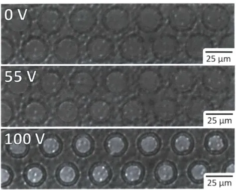
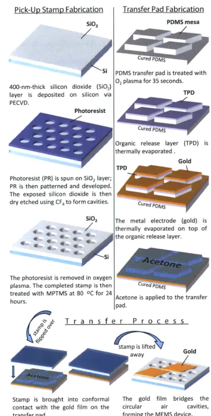
actuation, as the voltage applied is increased. The membrane is being imaged from the back of the device, through the transparent, ITO-coated glass substrate. The membrane pulls in at voltages greater than 90 V. . 51
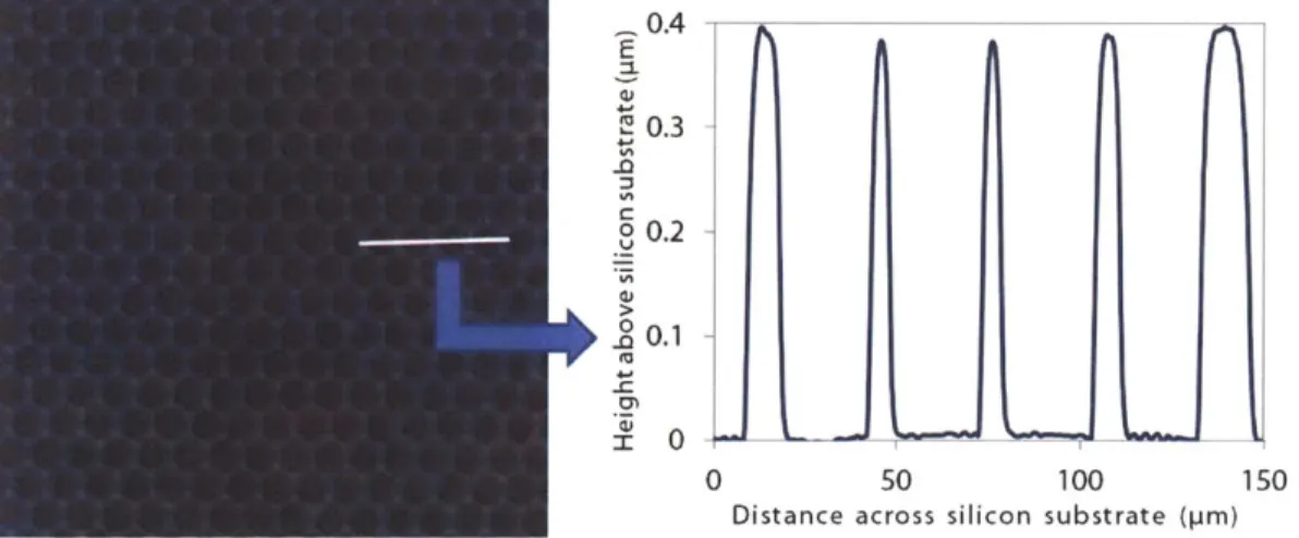
5.1 The process flow for the acetone-assisted, contact-transfer MEMS print-ing process on silicon-based substrates. The drawprint-ings above are not to scale. . . . .. . . . .. . . . . 60 5.2 A contact profilometry scan of the pick-up stamp. The pick-up stamp
consists of a 400 nm thick silicon dioxide spacer layer on a silicon sub-strate. The silicon dioxide spacer layer is patterned with circular cavities in a hexagonal-close-packed arrangement. . . . . 61
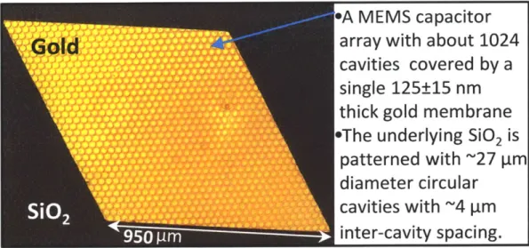
6.1 Optical microscopy image of a ~0.8mm2 area gold membrane MEMS de-vice printed on silicon dioxide using the acetone-assisted contact-transfer process. . . . . 64
6.2 Deflection profiles of gold membranes under electrostatic actuation, ob-tained via optical interferometry. The height values shown above are offset by about 60 nm due to the presence of transparent oxide in the cavity reference region used by the interferometer. The deflection val-ues, however, are absolute, i.e., about 60 nm should be subtracted from each point on each deflection curve above. (a) Deflection of the mem-brane increases as the voltage applied between the memmem-brane and the Si substrate increases. (b)13 different diametrical deflection profiles (inset: interferometry image) of a membrane under 15 V actuation, are plotted and averaged to show the mean profile. (c) Gold membrane deflection over multiple cavities covered by a single membrane, as the voltage is increased from 1 V to 15 V. . . . . 66 6.3 Optical interferometry images of several cavities under 15 V
peak-to-peak amplitude sinusoidal voltage actuation at 15 Hz, taken at 300 phase intervals. Membrane deflection for only one half of a sine wave is shown in this figure. Each cavity is about 27 vm in diameter. . . . . 67
6.4 A 3-D image of a gold film deflected over circular cavities, obtained using
optical interferometry. The maximum deflection of the gold film is about
150 nm in the center, under 15 V bias. The diameter of each circular
cavity is about 27 pm . . . . 68 6.5 Equation 6.1 fitted to the profile of a deflected membrane at 15 V bias,
7.1 An optical interferometry image of a 630 im x 473 jm region of a gold film transferred onto a planar silicon substrate, without any tilt correc-tion. This region of the transferred film has an average surface roughness of 9.24 nm and a root mean square roughness of 11.45 nm. . . . . 75
7.2 An optical interferometry image of a 630 pm x 473 pum region of a gold film (as shown in Figure 7.1), with tilt correction applied. The average surface roughness of the same region decreases to 1.94 nm, and the root mean square roughness decreases to 3.03 nm when tilt correction is applied. 76
7.3 Optical interferometry images of the same transferred gold film taken at different magnifications. (a) A 1.2 mm x 0.87 mm region of a transferred gold film with an average surface roughness of 2.27 nm and a root mean square roughness of 3.61 nm. (b) A 319 Im x 239 pm region of the same film with an average surface roughness of 1.81 nm and a root mean square roughness of 3.03 nm. (c) A 630 pm x 473 pm region of the same transferred gold film with an average surface roughness of 1.94 nm and a root mean square roughness of 3.03 nm, as shown in Figure 7.2 also.
(d) A 50 pm x 48 pm subregion of the film in (c) that is largely free
from processing residue or specks. The average surface roughness of this subregion is reduced to 1.32 nm and the root mean square roughness is reduced to 1.60 nm . . . . . 78
7.4 An optical interferometry image of a gold film contact-printed onto a cavity-patterned silicon dioxide spacer layer. Two main types of defects are observed. The gold film collapses over some cavities as it sticks to the cavity sidewalls and to the cavity bottom. This collapse of the gold film causes it to stretch irreversibly. The uncollapsed gold film over a cavity is excessively stretched when that cavity is surrounded by other cavities over which the gold film has collapsed. The excessive stretching causes the gold film to take on a peculiar shape, best described as a 'ridge' surrounded by a 'basin' on either side. The direction of the ridge is determined by the direction of excessive tension. Therefore, the ridge usually runs between two cavities with collapsed gold films, as shown above. If a cavity is surrounded by more than two cavities with collapsed membranes, then the direction of the ridge over the 'sandwiched' cavity is offset to account for the excessive tension from the surrounding
collapsed-m ecollapsed-m brane cavities. . . . . 79 7.5 An optical interferometry image of a gold film that has collapsed over one
of the cavities during the fabrication process. The thin green ring near the perimeter of the cavity indicates that the sunk-in gold film is nearly vertical at the cavity perimeter, as corroborated by the cross-section profile in Figure 7.6. . . . . 80 7.6 Cross-section profiles of a gold membrane that has collapsed over a
cav-ity during the fabrication process. The vertical distance from the gold membrane on top of a silicon dioxide support (in between adjacent cav-ities) to the gold membrane at the bottom of a cavity is about 950 nm, as indicated above. This implies that the gold membrane sinks all the way to the bottom of the cavity. . . . . 81
7.7 Optical interferometry images of an over-stretched gold film over a 'sand-wiched' cavity, as shown in Figure 7.4. The cavity shown is surrounded
by two cavities (not shown) over which the gold film has collapsed
dur-ing the fabrication process. (a) A 2-D image of the sandwiched cavity.
(b) A 3-D image of the sandwiched cavity obtained using
interferome-try data to highlight the elevated regions (the ridge) and the depressed regions (the basins) of the over-stretched gold film. The ridge spans the diameter of the cavity, and the two surrounding cavities over which the gold film has collapsed, are at either end of the ridge, as indicated by the points A and A' on the figure. . . . . 83
7.8 Cross-section profiles of the over-stretched gold membrane across a sand-wiched cavity, as discussed in Figure 7.7. The profile in red is across the basins and the ridge of the gold membrane, showing that the ridge rises about 200 nm above the planar surface of the gold film and that the deepest point in the basins is about 300 nm below the planar surface of the gold film resting on the silicon dioxide supports. The profile in blue is across the length of the ridge. . . . . 84
7.9 (a) Optical interferometry image of a gold membrane deflected over 400 nm deep cavities under 15 V applied bias. The white line indicates the cavities for which the deflection is plotted in (b) over various applied voltages. This line of cavities (A-E) is next to a cavity over which the gold membrane has collapsed due to fabrication, as indicated by 'X'. (b) Gold membrane deflection over multiple cavities as the voltage applied is increased from 1 V to 15 V. The deflection of the gold membrane over a cavity (E) next to a collapsed-membrane cavity (X) is significantly smaller than that of the membrane over cavities (A-D) further away from the collapsed-membrane cavity. . . . . 85
8.1 Photographs of large area gold membrane devices fabricated on cavity-patterned silicon dioxide substrates via acetone-assisted contact-transfer printing with increased transfer pad curing time and spacer layer silaniza-tion time, increased silane concentrasilaniza-tion, and increased silanizasilaniza-tion tem-perature. (a) A large area gold membrane covering about 16000, 2 7-pm-diameter cavities, in a single-sensor geometry. (b) and (c) Arrays of large area gold membranes, each covering about 4000, 27-pm-diameter cavities. . . . . 90
8.2 Photographs of two approximately 0.5" x0.5" silicon substrates that are extensively covered in gold films transferred via the modified acetone-assisted contact-transfer process. The yield (the area of gold picked-up and transferred per substrate) increases significantly due to the modifi-cation of transfer pad fabrimodifi-cation and spacer layer silanization parameters. 90
8.3 The electrical setup for preliminary sound production tests. The signal is being applied to the contact-printed device from the waveform generator via a high voltage amplifier. Electrical contact to the device is made using soft gold wire probes. Silver paste is used to improve electrical contact between the device substrate and the grounded aluminum foil. 91 8.4 The far-field beampattern for an unphased, two-dimensional,
rectangu-lar array of sound producing elements obtained by computing the 2-D discrete Fourier transform (DFT) of the rectangular array. The narrow main lobe in the beampattern suggests that the loudest sound is heard on-axis, that is, directly above the gold film of the contact-printed device. 92
8.5 A cross-section schematic of a MEMS device with a contact-printed
metal film. The thickness of the film varies across the length of the film such that multiple cavities or gaps are bridged by a single fihn of varying thickness. The bridged cavities can be commonly actuated or each cavity can be addressed individually. The drawing above is not to scale. . . . . 9 4
9.1 An illustration of a large-area array of individually-addressable sensors (or actuators) fabricated on a flexible substrate. Each element in the array can be addressed via the row-selecting and column-selecting mul-tiplexers. . . . . 98 9.2 A simple current-sensing circuit implemented using an op-amp
differen-tiator to detect capacitance changes of the MEMS device in response to an incident sound pressure wave. . . . . 99
9.3 When the deflection, h, of the metal membrane is large enough, a sig-nificant portion of the reflected light intensity decreases due to inter-ference, thus making the membrane covered surface appear rough. The devices discussed in Chapter 6 are able to achieve deflections that are large enough to produce the aforementioned effect for a wide spectrum of visible light, for angles of incidence up to 60 . . . . . 101
9.4 The blue arrows represent incident light and the black arrows represent reflected light. The metal membrane can be made to deflect asymmet-rically by switching ON only one of the two electrodes, A or B. The asymmetrical deflection causes the normal of the reflecting surface to ro-tate, hence, changing the direction in which the incident light is reflected. The degree of asymmetrical deflection can be increased or decreased by increasing or decreasing the voltage applied to the ON electrode. When both electrodes are switched on or switched off, most of the incident light is reflected back in the incident direction. . . . . 103
List of Tables
9.1 The minimum uniform deflection of metal membranes needed to make a reflecting surface appear rough through diffused reflection, for red, green, and blue light, at different angles of incidence of light. . . . . 102
Chapter 1
Microelectromechanical Systems
Microelectromechanical systems (MEMS) are devices that have components on the order of 1 micrometer to 100 micrometers in size that are typically fabri-cated on a silicon substrate. MEMS encompass a wide range of electronic sensors and actuators such as accelerometers, gyroscopes, pressure sensors, chemical sen-sors, etc. These devices are ubiquitous in consumer electronics such as hand-held gaming devices, gaming controllers, cellular phones, and camera-lens stabilizers. Accelerometers and gyroscopes are also used for vehicular stability and control in cars. MEMS also have a variety of industrial applications for precise measurement of linear and rotational motion and detection of forces, air and gas pressures, and other physical phenomenon. It is desirable to extend the functionality of MEMS to different form factors including large area arrays of sensors and actuators, and various substrate materials. Large area MEMS consist of arrays of numerous MEMS devices fabricated on a single substrate. Each MEMS device in an array acts as an individual sensor and senses the physical phenomenon such as force or pressure in its immediate local area. Therefore, all the sensors in a large area array can provide information about the physical phenomenon as it varies across
the large area of the array. However, scalable large area MEMS have yet to be fabricated cost-efficiently, and on substrates other than silicon. Large area MEMS arrays have a variety of potential applications-they can be used as phased-array sensors for acoustic imaging, as sensor skins in humans and vehicles, and for wind-tunnel testing [11. Conventionally, pressure sensors are placed at a finite number of points on a surface of a body that is being tested in a wind-tunnel. The data from these finite number of pressure sensors is then extrapolated to deduce the air pressure conditions at areas between the pressure sensors. Large area MEMS arrays reduce the need for the extrapolation of sensor data due to the high spatial resolution of the sensors in these arrays, thus enabling pressure to be sensed across the surface of the body with greater accuracy. Additionally, in order to fabricate large-area sensor arrays that can act as sensor skins and conform to the shape of the vehicle or the human body, it is desirable to fabricate these arrays on a flexible substrate, such as polymeric substrates [11.
Even though MEMS on scalable, large area substrates or on flexible substrates are desirable and have a great variety of potential applications, standard MEMS fabrication processes are incompatible with plastic substrates. Conventional fab-rication of MEMS devices involves processes that are typically used in microelec-tronics fabrication [1], and are centered around using silicon as the substrate upon which these devices are fabricated [2]. Processing of silicon to fabricate MEMS devices often involves photolithography, harsh chemical etches, and elevated tem-perature processing [1] for the growth of oxides and the deposition of polysilicon. Additionally, since conventional microelectronics fabrication is limited to conven-tional silicon wafer sizes [3], it is difficult to scale the area of arrays of MEMS sensors to any particular size. Moreover, the harsh chemical etches and the el-evated temperature processing make it difficult to fabricate MEMS devices on
flexible substrates that degrade under such processing.
Fabrication of flexible electronics using silicon processing techniques involves fabricating the electronics on a silicon substrate and then bonding these structures to flexible sheets. These structures are then released from the silicon substrate by breaking small supports or by etching away a sacrificial layer [4]. However, this process has not been used for MEMS fabrication.
1.1
Microcontact Printing of MEMS
Printing techniques which involve flexible polymeric stamps, like the ones em-ployed by Rogers [4][5], fall under the more general category of microcontact printing or soft lithography. Such techniques show promise for the patterning or transfer of microscale films of a variety of materials. Microcontact printing can be utilized for the fabrication of large area MEMS arrays on a variety of substrates, including silicon. The approach to microcontact printing presented here involves the use of a stamp and a donor transfer pad. The donor transfer pad consists of a viscoelastic material coated with an organic release layer. A thin film of metal is then deposited on top of the organic release layer via evaporation. The stamp consists of a layer of patterned PDMS atop a glass slide that is coated with a layer of electrically conducting indium tin oxide (ITO). The surface of this patterned
PDMS stamp is placed in contact with the thin metal film on the donor transfer
pad and then the stamp is rapidly peeled away, picking up the metal film. The metal film ends up bridging the gaps in the patterns of the PDMS stamp, forming a capacitive MEMS structure. A continuous film of metal is lifted off onto the stamp only if the stamp is peeled off from the transfer pad rapidly, as discussed in References [4] [5], where it is shown that a rapid peel rate greater than 5 ms1
en-mnetal from inkpad
7.
mumm """""*ITOVISCOELASTIC SUBSTRATE VISCOELASTIC SUBSTRATE GLASS GLASS
Figure 1.1: An overview of the microcontact printing process. The stamp consists of a PDMS layer that has been patterned with ridges that are about 25 Vm wide, with 25 Vm spacings between the ridges. The transfer pad consists of a viscoelastic substrate, such as PDMS, coated with an organic release layer, upon which a thin film of metal has been evaporated. The stamp is brought into contact with the metal film on the transfer pad, and it is rapidly peeled away, picking up the metal film from the transfer pad. The metal film bridges the gaps across the ridges in the PDMS if the stamp is peeled away from the donor transfer pad fast enough. The diagram above is not drawn to scale.
hances adhesion between a viscoelastic polymer and silicon thin film components and allows these thin film components to be lifted off from the substrate and onto the viscoelastic polymer.
Microcontact printing does away with the harsh chemical etches and the el-evated temperature processing typical of conventional MEMS fabrication tech-niques. In fact, most of the processing after the organic and metal deposition can be carried out at room temperature and pressure conditions. This enables the use of a variety of substrates that would otherwise degrade at high temperatures and pressures, such as flexible polymeric substrates. Additionally, since we are no longer restricted to silicon substrates, the size of the substrates can be scaled easily, enabling the fabrication of large-area sensor arrays.
1.2
Prior Work and State of the Art
In the Bulovic research group, we demonstrate the fabrication of a MEMS capaci-tor structure using the contact lift-off transfer (Contact-Transfer) technique. The
Contact-Transfer technique relies on the rapid removal of the patterned PDMS stamp from the donor transfer pad to effect the transfer of a continuous film of gold from the donor transfer pad to the patterned PDMS stamp. The rapid
re-moval of the patterned PDMS stamp is essential for the transfer of a continuous
gold film because the adhesion )etween the gold film (on the transfer pad) and the PDMS ridges on the stamp is enhanced by a rapid peel rate. The removal of the gold thin film from the transfer pad is also enhanced due to the weak van der Waals bonding between the gold film and the organic release layer underneath it on the transfer pad. This weak van der Waals bonding between the gold film and the organic release layer is overcome by the kinetically controlled adhesive forces between the PDMS ridges and the gold film, allowing the transfer of a continuous film of gold that bridges the gaps between the PDMS ridges on the stamp. This continuous gold film atop the air gaps between the PDMS ridges is flexible and it can deflect in response to pressure. The resulting structure is a variable capaci-tor that can be used as a MEMS device for sensing acceleration, pressure, sound waves, and other physical phenomenon.
The organic used for the release layer is N,N'-diphenyl-N,N'-
bis(3-methylphenyl)-(1,1'-biphenyl)-4,4'-diamine (TPD). The TPD organic release layer is 90 nm thick
and the gold film is ~140 nm thick. The above technique is demonstrated for three different sets of stamps. The first set of stamps has PDMS ridges that are 45 vm wide, 25 vm apart and 1.2 vm high, with an underlying layer of PDMS that is 1.8 rm thick. The second set of devices has PDMS ridges that are 20 vm wide, 20 pm apart and 2.2 im high, with an underlying layer of PDMS that is 12 tm thick. Both of these stamps are fabricated on an ITO-coated glass substrate. The third set of stamps is fabricated on a flexible, ITO-coated, 175-tm-thick polyethylene terephthalate substrate [1]. Refer to Figure 1.2 for fabrication details. The oxygen
plasma exposure time for the flexible substrate is reduced to 1 minute. All other fabrication steps for the flexible substrate devices are the same as those for the glass substrate devices.
Using the above-mentioned process flow, we fabricate a variable capacitor structure whose capacitance varies from about 4.4 pF to 4.8 pF as the voltage is swept from 0 V to 100 V, as shown in Figure 1.3. The resulting devices are shown in Figure 1.4.
The fabricated MEMS variable capacitor can be used to sense air and gas pressures. Thus, the next step is to model these capacitors as pressure sensors that are capable of producing a measurable change in capacitance in response to a range of applied pressures. Once the MEMS capacitors are modeled as pressure sensors, a fabrication process is designed for fabricating these devices using microcontact printing. Additionally, the fabrication steps are improved to remove the edge effects that are present at the edges of the lifted-off gold membranes, as seen in Figure 1.4. The poor edge-definition compromises control of the device geometry. The edge-definition is poor because the gold membrane decreases in thickness at its edges due to the deposition of the gold on the donor transfer pad via a shadow mask. The current process, termed mesa-transfer, reduces the edge roughness of the lifted-off gold membrane, and is used to fabricate capacitive MEMS structures. These micro-contact printed structures are then characterized as pressure sensors
by demonstrating the deflection of the printed gold membranes via electrostatic
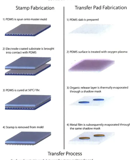
Contact-Transfer
Stamp Fabrication
1) PDMS is spun onto master mold
2) Electrode-coated substrate is brought into contact with PDMS
3) PDMS is cured at 50*C/1 hr.
4) Stamp is removed from mold
Transfer Pad Fabrication
1) PDMS slab is prepared
2) PDMS surface is treated with oxygen plasma
3) Organic release layer is thermally evaporated
through a shadow mask
4) Metal film is subsequently evaporated through the same shadow mask
Transfer Process
Conformal contact is made between the stamp and transfer pad.
Transfer of the metal film is achieved by rapidly peeling the stamp from the transfer pad.
Figure 1.2: Process flow for contact lift-off transfer, as demonstrated by Packard, Mu-rarka, et al. The last picture in the process flow shows that the PDMS ridges on the stamp are bridged by the lifted-off gold membrane, with air gaps between the ridges and beneath the membrane. The resulting MEMS variable capacitor can be used as a component of a variety of sensors [1].
6 4.7. 1 mm diameter devices 4.5-C- Device 2 4.3 0 10 20 30 40 50 60 7 8 9010 Voltage (V)
Figure 1.3: Capacitance-voltage measurements for two devices (inset: geometry) tested as MEMS variable capacitors. As the voltage across the device increases, the electrostatic force of attraction between the gold membrane and the ITO electrode increases, causing the gold membrane to bow. The bowing of the gold membrane decreases the spacing between the two electrodes of the capacitor, hence, increasing the capacitance. Image courtesy [1]. a) b) Transferred gold membrane Electrode C)
Figure 1.4: Images of the devices formed by the Contact-Transfer process. a,c) Optical microscopy images of completed devices that act as variable capacitors. b) A schematic of completed devices. d) Photograph of devices fabricated on a flexible substrate
[1].
Chapter 2
Modeling of PDMS Spacer Layer
Pressure Sensors
The variable capacitor MEMS structure fabricated via microcontact printing can be used to sense pressure as the gold membrane of the structure deflects in response to applied pressure, hence changing the capacitance of the device. These MEMS variable capacitors are modeled as pressure sensors that are capable of producing a measurable change in capacitance for a range of applied pressures. This implies that the membrane of the variable capacitor should be able to bow enough to produce a measurable change in capacitance under pressures between 2 psi to
30 psi, without breaking, or losing its elasticity. The pressure range is chosen
to reflect the conditions most commonly encountered in wind-tunnel testing, with the aim that these devices might eventually be suitable for fabricating sensor skins for vehicular wind-tunnel testing.
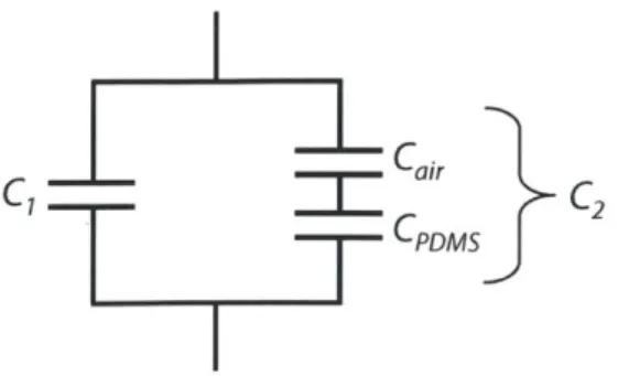
The pressure sensor MEMS device is modeled as a circular cavity in a PDMS spacer layer that sits atop an ITO-coated glass substrate. This cavity is bridged
to air pressure, as shown in Figure 2.1. The circular air cavity and its PDMS supports are electrically modeled as two capacitors, C, and C2, in parallel with each other, as shown in Figure 2.2. Capacitor C, comprises the capacitance of the PDMS support structures that surround the air cavity in the PDMS layer. This capacitance is assumed constant and it does not change in response to applied pressure. Capacitor C2 consists of the capacitance of the air gap, Cair, in series with the capacitance of the underlying residual PDMS layer, CPDMS. This residual PDMS layer tends to act as a dielectric layer in capacitor C2. The capacitance
Cair changes in response to applied air pressure.
k radius, r
h
d
surrounding PDMS support structure
Figure 2.1: A cross-sectional schematic of the air cavity and the surrounding PDMS support structure, being bridged by a gold membrane. The diagram is not drawn to scale.
C, C2
Figure 2.2: An electrical model of the air cavity and the surrounding PDMS support structure shown in Figure 2.1.
The capacitance of C, is given by,
C
O EPDMSAsupport
8.854 x 10⁻¹² 2.55 -Asuppor
1
d
,(2.1)
where F0 = 8.854 x 10⁻¹² (permittivity of free space), 6PDMS = 2.55 (dielectric
constant of PDMS [6]), Asupport is the area of the PDMS supports surrounding the circular cavity, and d is the distance between the top and bottom electrodes as
defined in Figure 2.1.
The capacitance of C2 is given by,
C2 = 6 FPDMS Amembrane (2.2)
EPDMS (d
- t) + twhere d is the distance between the top and bottom electrodes, t is the thickness of the residual PDMS layer in the air cavity as defined in Figure 2.1, and Amembrane is the area of the circular gold membrane that can deflect.
Since capacitances in parallel add, the net capacitance, Cdevice, of the air cavity and its surrounding PDMS is given by,
COevice = C1 + C2 = 6 EPDMS
Asupport
60 E PDMSAmembrane
d
ePDMS (d -(2.3)
If the circular cavity has a diameter of 1 mm and a surrounding annular PDMS
support structure of width k = 0.1 mm, then substituting d = 5 vm and t = 3 im into Equation 2.3 yields a device capacitance, Cdevice, of about 3.7 pF. A 0.1 pF change in the capacitance of the above-modeled air cavity is desired when pressure is applied because a change of 0.1 pF can be measured easily by test circuitry. Assuming uniform deflection of the gold membrane across its entire area-that is, the gold membrane deflects by equal amounts everywhere across its surface-then
a deflection of about 140 nm is needed to observe a change of 0.1 pF. However, in reality, when pressure is applied on a circular membrane, it deflects the most at its center and the least towards its edges. Hence, in reality for a 140 nm deflection of the gold membrane at its center, a change in capacitance of less than 0.1 pF for the whole device is expected.
The deflection of a circular membrane (that is supported at its edges) of radius
r, when a uniformly distributed force is applied perpendicular to the plane of the
membrane is shown in Figure 2.3 [7]. The membrane is assumed to be under tension before the force is applied. Additionally, it is also assumed that the
deflection is purely elastic and recoverable, with no permanent deformation.
k radius, r
circular air cavity d
residual PDMS layer
--- __-- surrounding PDMS support structure
Figure 2.3: When pressure is applied perpendicular to the plane of the circular mem-brane, it deflects. The naxinum deflection, Wmax, occurs at the center of the circular membrane. This figure is not drawn to scale.
The maximum deflection, Wmax, at the center of a circular membrane of radius r, is given by,
(5 + v) q r'
Wmax=,(24
64 (1+ v) D
where q is the pressure distributed uniformly over the circular membrane surface, D is the flexural rigidity of the membrane, and v is the Poisson's ratio for gold (v
The flexural rigidity of the membrane, D, in Equation 2.4 is given by,
E ha
D =- E (2.5)
12(1 - v2
) '
where E is the modulus of elasticity of gold (E 78 GPa), h is the thickness of
the gold membrane, and v is the Poisson's ratio for gold.
For an applied pressure of 10 psi, using the device geometries stated above for a 3.7 pF air cavity with surrounding PDMS supports, substituting q = 10 psi, r = 0.5 mm and h = 140 nm into Equations 2.4 and 2.5, yields a maximum deflection
of 11.8 meters-a displacement that is significantly in excess of the air gap height and is, therefore, an unphysical result. Instead, a maximum deflection of about 150 nm is desired to reduce the likelihood of membrane rupture. Therefore, in order to decrease the maximum deflection of the gold membrane, the radius of membrane needs to be reduced by two orders of magnitude, the pressure applied needs to be reduced, and the flexural rigidity of the gold membrane needs to be increased by increasing the thickness of the gold membrane to about 200 nm. Thus, if h = 200 nm and the applied pressure, q, varies between 2 psi to 10 psi, the radius of the gold membrane needs to be between 7 tm and 10 vm for a maximum membrane deflection of 150 nm under the applied pressure. However, reducing the radius of the gold membrane from 0.5 mm to 10 rm greatly reduces the area of the variable capacitor that consists of the air cavity. The capacitance, Cdevice, of the air cavity and the surrounding annular PDMS supports is reduced by about three orders of magnitude to 2.1 fF as the radius of the cavity is reduced from 0.5 mm to 12.5
min. This means that when the membrane deflects by 150 nm, only ~6.8 x 10⁻¹ F of capacitance change results. We require around 0.1 pF of capacitance change for the same amount of deflection when 2 psi to 10 psi of pressure is applied.
Since capacitances add up in parallel, the changes in capacitances also add up. Thus, a multitude of these smaller air cavities can be arranged in parallel with each other to achieve the desired change in capacitance for ~150 nm of deflection under applied pressure. The air cavities can be electrically connected in parallel
by covering them with a common gold film electrode. About 1500 of the
above-modeled air cavities are needed in parallel with each other to form a single pressure sensor that is capable of providing a net 0.1 pF of capacitance change in response to a 150 nm membrane deflection in each of these 1500 cavities when 2 psi to 10 psi of pressure is applied.
It is necessary to pack all of these air cavities in as small a space as possible in the PDMS spacer layer atop the ITO-glass, in order to minimize the non-active capacitance due to the PDMS supports surrounding these air cavities. An efficient way to pack circular air cavities in a two dimensional plane is to use hexagonal close packing with a certain amount of fixed spacing between the perimeters of each of the air cavities, as shown in Figure 2.4. The gold film covering the air cavities has a parallelogram shape so that it can completely cover the maximum number of cavities while minimizing the capacitance from the surrounding PDMS spacer layer.
A 32x32 array of hexagonal-close-packed 1024 air cavities (each with a radius
of 12.5 m) with -a spacing, s, of 5 vm between the cavities, will have a total
capacitance of 2.7 pF. A MEMS device comprising 1024 cavities will give a total of approximately 0.07 pF capacitance change when the gold membrane deflects
uniformly by 150 nm. This 32x32 array will have a total area of 0.79 mm2, including the PDMS supports in between the air cavities. A 16x 16 array of 256 hexagonal-close-packed air cavities will a total area that is a quarter the area of a 32x32 array. As a result, the capacitance of a 16x 16 array with the same
Gold film ZHexagonal-close-packed
circular air cavities in PDMS
Figure 2.4: We can group many small air cavities together in a PDMS substrate and electrically connect them in parallel by covering them with a common gold film electrode. The gold film is a parallelogram in shape so that it can completely cover the maximum number of air cavities while minimizing the capacitance from the surrounding PDMS. The figure is not drawn to scale.
cavity radius and inter-cavity spacing (as a 32x32 array) will have a capacitance that is a quarter of the capacitance of a 32 x 32 array. A 16 x 16 array will give a total of approximately 0.0175 pF of capacitance change when the gold membrane deflects by 150 nm. For the initial device fabrication run, a 12.5 vm cavity radius
(r), and a 5 vm inter-cavity spacing (s) is selected. These devices are used as a
proof of concept and their characterization will enable more accurate modeling and fabrication of subsequent devices.
Chapter 3
MEMS Fabrication on PDMS
Spacer Layers
3.1
Photolithography Transparency Masks
The first step in the device fabrication process involves making the transparency masks that define the device (pressure sensor) geometries. These masks are used in ultraviolet (UV) photolithography for patterning photoresists. UV
photolithog-raphy is used for making SU-8 masters, which are in turn used as molds for patterning the PDMS transfer pad and the PDMS spacer layer on the ITO-glass pick-up stamp. SU-8 is a negative photoresist. The portion of SU-8 resist that is exposed to light becomes insoluble to the SU-8 photoresist developer, propylene glycol monomethyl ether acetate (PGMEA). The unexposed portion of the SU-8 resist is dissolved away by the SU-8 developer. Two different transparency masks are made.
Mask A is designed to mold raised parallelogram mesas on the PDMS transfer pad. Thus, Mask A has dark parallelogram regions of varying areas. These dark
parallelogram regions on the mask result in parallelogram troughs in the
SU-8 master, that in turn form raised parallelogram mesas on the PDMS transfer
pad. Mask A has dark rhombuses of two different areas-0.79 mm2 and 0.1975
mm2
. The internal angles of these rhombuses measure 600 and 120' to maximize
the number of hexagonal-close-packed air cavities completely covered by each rhombus. Mask A is printed at a resolution of 5080 dpi by PageWorks (Cambridge,
MA).
Mask B is designed to form circular air cavities in the PDMS spacer layer that is spun onto the ITO-glass stamp. Thus, cylindrical pillars need to be formed in the corresponding SU-8 master. Therefore, Mask B has transparent circular regions in a dark background. The transparent circles of 12.5 vm radius are hexagonal-close-packed with a minimum spacing of 5 im between adjacent circles. Mask B is printed at a 65024 dpi resolution by FineLine Imaging (Colorado Springs, CO).
3.2
SU-8 Master Molds
SU-8 photoresist (MicroChem Corp., SU-8 3010) is spun onto two different silicon
wafers separately to fabricate the SU-8 master molds for the pick-up stamp and the transfer pad. SU-8 photoresist is poured onto each silicon wafer and the wafer is spun at 1000 rpm such that the SU-8 covers the entire surface of the wafer. These wafers with the SU-8 layers are then spun at 3000 rpm for another 30 seconds, after which they are soft-baked on a hot plate at 95 'C for 5 minutes. Next, the wafers are allowed to cool for 2 minutes before being placed in an Amergraph UV exposure unit with either Mask A or Mask B placed on top of the SU-8 photoresist layer, with the mask emulsion in contact with the SU-8 layer. Mask A is used to make the SU-8 masters for the transfer pad and Mask B is used to make the
SU-8 masters for the pick-up stamp. The SU-8 photoresist is then exposed to UV
light. After UV exposure, the wafers are baked on a hot plate for 2 minutes. The wafers are then immersed in SU-8 developer solution (PGMEA) for 4 minutes and agitated. After that, the wafers are sprayed with PGMEA for 10 seconds to rinse off residual SU-8, and with isopropanol for another 10 seconds to remove
PGMEA. The wafers are dried with nitrogen and hard-baked for 3 hours at 150
C on a hot plate to get the resulting SU-8 masters. Following the hard bake, both
SU-8 master molds are silanized with trichloro(1H,1H,2H,2H-perfluorooctyl)silane
(Sigma-Aldrich) to ensure easy removal of the cured PDMS [1].
3.3
Pick-up Stamp Substrates
Next, an indium tin oxide (ITO) coated glass slide is cleaned using the standard substrate cleaning procedure: sonication in Micro-90 for 5 minutes, followed by sonication in deionized water twice for 5 minutes each, followed by sonication in
acetone twice for 2 minutes each, and followed by immersion in boiling isopropanol twice, for two minutes each. The ITO-glass slide is then blown dry with nitrogen and treated with oxygen plasma for 5 minutes. The pick-up stamp is fabricated by spinning uncured PDMS (Sylgard 184, Dow Corning Co.), mixed in a 10:1 base-to-curing-agent ratio by weight and degassed under vacuum, onto the silanized
SU-8 master with cylindrical pillars (made using Mask B). The conducting side
of the ITO-coated glass slide is then pressed firmly onto the spun PDMS atop the SU-8 master. The resulting structure is then placed in an oven at 60 C for 4 hours to cure the PDMS between the SU-8 master and the ITO-glass. The pick-up stamp with circular air cavities in the cured PDMS layer is then removed from the SU-8 master.
Figure 3.1: An optical microscopy image of a pick-up stamp before pick-up of gold membrane. Each circular air cavity in the PDMS layer is about 12.5 im in radius, and there is a spacing of at least 5 im between the perimeters of adjacent cavities.
3.4
Transfer Pad with Raised Mesas
The transfer pad is fabricated by pouring PDMS (Sylgard 184, Dow Corning Co.),
mixed in a 10:1 base-to-curing-agent ratio by weight and degassed under vacuum, onto the silanized SU-8 master with parallelogram troughs, in a Petri dish. The PDMS is then cured in an oven at 50 *C for 6 hours. The cured PDMS transfer pad is then peeled from the SU-8 master. This transfer pad has raised parallelogram mesa structures that rise above the plane of the PDMS substrate (refer to Figure
3.3). The mesas aid with the patterning and transfer of the gold electrodes because
thermal evaporation is a line-of-sight process, and it is not conformal.
After the curing process, the transfer pad is exposed to oxygen plasma (100W, Plasma Preen, Inc.) for 30 seconds, after which a 90 nm thick organic release layer
of N,N'-diphenyl-N,N'-bis(3-methylphenyl)-(1,1'-biphenyl)-4,4'-diamine (TPD,
Lu-minescence Technology Co.) and a 140 nm or 150 nm thick layer of gold are deposited in sequence via thermal evaporation [1] onto the transfer pad to define the gold electrodes on the parallelogram mesas of the transfer pad. The thin
gold film, vacuum-evaporated on top of the parallelogram mesas, breaks along the sharp edges of the mesas, hence, defining a gold film in the shape of the parallel-ogram. Therefore, the raised areas on the transfer pad define, with sub-micron resolution, the shape of the gold electrodes that are lifted-off onto the pick-up stamps because it is the raised areas that come into conformal contact with the
pick-up stamp.
4
93.58!~
Figure 3.2: An optical microscopy image showing a raised parallelogram PDMS mesa on a PDMS transfer pad, before TPD and gold are evaporated on it. The gold electrode picked-up from this mesa will cover about 256 circular air cavities, each of radius 12.5 tm. The same transfer pad also has bigger parallelogram mesas that have areas that are four times larger than the area of the mesa shown above.
3.5
Contact Lift-Off Transfer
Following the thermal evaporation, the pick-up stamp with circular air cavities is brought into contact with the gold film on the mesas of the transfer pad, and is rapidly lifted-off to peel away and transfer the gold film onto the stamp such that the parallelogram gold films cover the air cavities and form the top electrode of the pressure sensors, as shown in Figure 3.3. Figure 3.4 shows scanning electron micrographs of the SU-8 master mold, the transfer pad parallelogram mesa, the
pick-up stamp, and the transferred gold film. Figure 4.2 shows optical microscopy pictures of one of the devices fabricated using the described process.
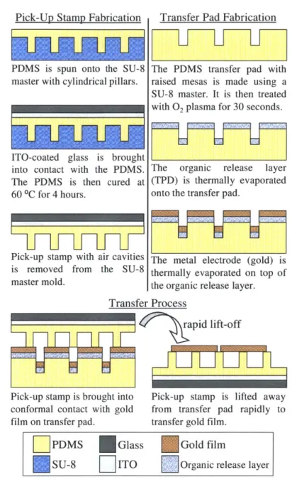
Pick-UD Stamo Fabrication . Transfer Pad Fabrication
PDMS is spun onto the SU-8 master with cylindrical pillars.
ITO-coated glass is brought into contact with the PDMS. The PDMS is then cured at
60 *C for 4 hours.
Pick-up stamp with air cavities is removed from the SU-8 master mold.
The PDMS transfer pad with raised mesas is made using a
SU-8 master. It is then treated
with 02 plasma for 30 seconds.
The organic release layer (TPD) is thermally evaporated onto the transfer pad.
The metal electrode (gold) is thermally evaporated on top of the organic release layer. Transfer Process
apid lift-off
Pick-up stamp is brought into conformal contact with gold film on transfer pad.
Pick-up stamp is lifted away from transfer pad rapidly to transfer gold film.
D
PDMS Glass Gold filmSU-8 ITO Organic release layer
Figure 3.3: The process flow for the contact lift-off mesa-transfer micro-contact printing process. The drawings above are not to scale.
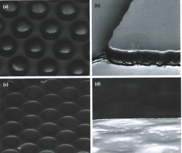
Figure 3.4: Scanning electron micrographs of (a) the SU-8 master mold, (b) a corner of the transfer pad parallelogram mesa with an organic film and a gold film evaporated on top, (c) the cavity-patterned PDMS spacer layer of the pick-up stamp, and (d) the edge of a transferred gold film bridging the air gaps in the PDMS spacer layer of the pick-up stamp.
Chapter 4
PDMS Spacer Layer Device
Characterization
Devices fabricated using the contact lift-off mesa-transfer process described in Chapter 3 have sharper gold film electrode edge definition than the devices fabri-cated using the shadow-masking process. The mesa-transfer process reduces the edge roughness of the gold electrodes to less than 1 Im, as shown in Figure 4.1. Additionally, the process demonstrates the ability to fabricate electrodes with sharp corners. Figure 4.2 shows a photomicrograph of a pressure sensor with two sharp corners fabricated using the mesa-transfer process.
The mesa-transfer process also has a qualitatively higher device yield than the shadow-masking process. The yield in the mesa-transfer process itself is affected
by the depth of the air cavities in the PDMS spacer layer between the gold and
the ITO electrodes. Devices with air cavity depths greater than 9 im have higher yield than devices with cavity depths less than 2 ym, because in the latter devices
the gold film comes into contact with, and sticks, to the PDMS at the bottom of the air cavities during the contact-printing step, just before lift-off, hence,
(a) Gold
Figure 4.1: Optical microscopy images contrasting the edge definition of devices fab-ricated using the old shadow-masking process and the new mesa-transfer process. a) Gold electrode of the MEMS device fabricated using shadow-masking. The edges of the electrode have poor definition. b) Gold electrode of the MEMS device fabricated using mesa-transfer. The edges of the electrode are much sharper and have sub-micron edge roughness.
permanently deforming the device.
The electromechanical performance of the fabricated devices is also character-ized. The fabricated devices are actuated electrically to demonstrate that the gold membrane above the air cavities can deflect in response to a voltage applied be-tween the gold membrane (the top electrode) and the ITO (the bottom electrode). As the applied voltage increases, the electrostatic force of attraction between the top and bottom electrode increases, causing the gold membrane bridging the air cavity to deflect more and, hence, decrease the distance between the electrodes. The decrease in the distance between the two electrodes results in an increase in the capacitance of the device, allowing mechanical deflection to be sensed elec-trically. The mechanical deflection of the membrane in response to electrostatic actuation mimics the mechanical deflection of the membrane in response to pneu-matic loading. Thus, electrostatic actuation of the device is a convenient method for its electromechanical characterization.
A device comprising a 32 x 32 array of 1024 air cavities (in PDMS) covered by a
single gold electrode, is actuated with an Agilent 4156C Precision Semiconductor Parameter Analyzer to perform quasi-static capacitance-voltage (QSCV)
measure-Figure 4.2: An optical microscopy image of the pressure sensor fabricated using the contact lift-off mesa-transfer process. The gold parallelogram is the pressure sensor. Sags are visible in the gold membrane above the circular cavities. About 1024 circular cavities are covered by this parallelogram gold membrane which is about 140 nm thick. The mesa-transfer process enables the printing of sharp corners, with sub-micron edge roughness. The underlying PDMS on ITO-Glass is patterned with 25 Im diameter circular cavities with about 5 im to 7 im spacing between the circles. The circular cavities are arranged in a hexagonal-close-packed pattern.
ments. Electrical contact with the device electrodes is made using a compliant probe tip and gold wire. The gold-wire probe tip contacts the gold membrane of the device. The compliant probe tip contacts the ITO layer of the device which is exposed by scratching away some of the PDMS on the pick-up stamp. A voltage is applied between the top and bottom electrodes and increased in steps of 1.0 V. The resulting capacitance of the device is measured as a function of the applied voltage.
The results of the QSCV measurements over three runs on the same device are shown in Figure 4.3. The increase in the capacitance of the device with increasing voltage indirectly demonstrates deflection of the gold membrane, which bows under the electrostatic force to decrease the gap spacing over the air cavities in the PDMS spacer layer, thus increasing the capacitance.