HAL Id: hal-02345145
https://hal.umontpellier.fr/hal-02345145
Submitted on 4 Nov 2019
HAL is a multi-disciplinary open access
archive for the deposit and dissemination of
sci-entific research documents, whether they are
pub-lished or not. The documents may come from
teaching and research institutions in France or
abroad, or from public or private research centers.
L’archive ouverte pluridisciplinaire HAL, est
destinée au dépôt et à la diffusion de documents
scientifiques de niveau recherche, publiés ou non,
émanant des établissements d’enseignement et de
recherche français ou étrangers, des laboratoires
publics ou privés.
D. Díaz-Thomas, Oleksandr Stepanenko, M. Bahriz, Stéphane Calvez, E.
Tournié, A. Baranov, Guilhem Almuneau, L. Cerutti
To cite this version:
D. Díaz-Thomas, Oleksandr Stepanenko, M. Bahriz, Stéphane Calvez, E. Tournié, et al.. Interband
cascade Lasers with AlGaAsSb cladding layers emitting at 3.3 µm. Optics Express, Optical Society of
America - OSA Publishing, 2019, 27 (22), pp.31425. �10.1364/OE.27.031425�. �hal-02345145�
Interband cascade Lasers with AlGaAsSb
cladding layers emitting at 3.3 µm
D. A. D
ÍAZ-T
HOMAS,
1O. S
TEPANENKO,
2M. B
AHRIZ,
1S.
C
ALVEZ,
2E. T
OURNIÉ,
1A. N. B
ARANOV,
1G. A
LMUNEAU,
2 ANDL. C
ERUTTI1,*1IES, Univ. Montpellier, CNRS, F-34000 Montpellier, France 2LAAS-CNRS, 7 avenue du Colonel Roche, F-31400 Toulouse, France *[email protected]
Abstract: We investigate the impact of the growth conditions of AlGaAsSb cladding layers on the properties of interband cascade lasers (ICLs). For an optimized structure emitting at 3.3 µm, we achieve an internal quantum efficiency of 65% per stage in good agreement with conventional ICL using InAs/AlSb superlattice cladding layers, in spite of internal losses of 15 cm−1due to higher optical losses in the n-type AlGaAsSb alloys. Finally, we report a narrow ridge ICL emitting at 3.33 µm operating in continuous wave up to 80°C that produces 1 mW/uncoated facet at 80 °C, 10 mW at 40 °C and more than 12 mW at 20°C.
© 2019 Optical Society of America under the terms of theOSA Open Access Publishing Agreement
1. Introduction
The 3-5 µm wavelength range is of high interest for spectroscopy applications. The strong light absorption by hydrocarbons and other atmospheric pollutant gases, concomitantly with the high-transmissivity of water make this mid-infrared (MIR) spectral window very attractive for environmental monitoring. High-performance semiconductor lasers suitable for Tunable Diode Laser Absorption Spectroscopy (TDLAS) emitting in the MIR are then a key enabling technology for these applications, as well as for free-space communications and light detection and ranging (LIDAR) in this atmospheric window [1–4]. Over the last decade, significant progress in Interband Cascade Lasers (ICLs) [5,6] has allowed them to firmly bridge the gap between quantum cascade lasers (QCLs) [7,8] and GaSb-based type–I laser diodes [9,10]. Furthermore, their current performance make them very attractive for the development of portable and small footprint optical sensors for in-field applications. Indeed, ICLs exhibit low threshold current density and overall low-power consumption while maintaining an ability to generate high optical powers in continuous wave (CW) regime at room temperature (RT) and above [11–13].
To achieve such performance, the typical ICL design relies on an active region based on cascaded type-II “W” InAs/GaInSb quantum wells (QWs) [14] separated by hole and electron injectors, embedded between cladding layers made of InAs/AlSb superlattices (SLs) [15]. Although these SLs offer excellent electrical conductivity, they exhibit three drawbacks compared to bulk AlGaAsSb cladding layers, namely a relatively high refractive index (n∼3.4), a low thermal conductivity and a complex growth. Indeed, contrary to type-I GaSb laser diodes emitting in the 2 to 3.6 µm range which exploit Al-rich AlGaAsSb cladding layers (n∼3.3) [16], the SL-baring laser diodes show reduced optical confinement and thereby require thicker epitaxial stacks to successfully operate [12,17]. Furthermore, the laser thermal management is detrimentally affected by the thermal conductivity of InAs/AlSb superlattices (3 W/m.K) which is smaller than that of Al0.9Ga0.1AsSb (7 W/m.K) [18,19] and which can even be further affected by their multiple interface heat resistance. Finally, the epitaxial growth of the SL structures requires more than a thousand cell shutter actuations which not only contribute to the accelerated aging of parts of the epitaxy equipment but also require a careful growth control of the InAs/AlSb
#375171 https://doi.org/10.1364/OE.27.031425
interfaces which do not share any common atom [20]. On the contrary, the epitaxial growth of AlGaAsSb cladding layers by molecular beam epitaxy (MBE) is well mastered, as already demonstrated for GaSb-based diode lasers emitting between 1.55 µm to 3.7 µm [21,22,23]. The above-mentioned arguments suggest that ICLs including AlGaAsSb cladding layers would be amenable to deliver improved laser performance. However, the optimal temperature for the MBE growth of such Al-rich AlGaAsSb is typically above 500°C [24] whereas we have found that “W” type-II QWs should be grown at around 435°C to achieve both high crystalline quality and photoluminescence (PL) efficiency at RT, similarly to the results obtained by others [25]. This large optimal temperature difference unambiguously requires a compromise to get high performance lasers. Indeed, it has been demonstrated successfully that AlGaAsSb alloys can be used as cladding layers of ICLs [17]. In this latter reference, the two claddings were grown at 500°C and authors demonstrated ICL with threshold current density of 220 A/cm2and CW operation up to 45°C with an emission at 3.4 µm. One can notice, that the active structure was similar to the References 12 and 26 using AlSb/InAs SL as cladding layer which emit between 3.6 and 3.8 µm with threshold current density below 150 A.cm−2. The performance degradation in comparison to ICL with SL cladding layer was attributed possibly to the separate confinement layer thickness and growth conditions.
In this paper, we report a detailed investigation on the impact of the growth conditions of the top AlGaAsSb cladding layer on the performance of broad-area and narrow-stripe ICLs. 2. Structure design and MBE growth optimization
In this work, different sets of ICLs whose cladding layers are made of Al0.85Ga0.15As0.07Sb0.93 lattice matched to GaSb are studied. The optimal temperature for the MBE growth of such Al-rich AlGaAsSb is typically above 500°C [24]. Albeit, we have found that “W” type-II QWs should be grown around 435 °C to achieve both high crystalline quality and photoluminescence (PL) efficiency at RT, similarly as the results obtained in [25]. This large temperature difference between the optimal growth conditions of the cladding layer material and the underlying active region triggered the present study of the influence of the growth temperature of the top cladding layer on the ICL overall crystalline quality and laser performance. To investigate this matter, we grew four ICLs structures using different growth temperatures for the top cladding layer.
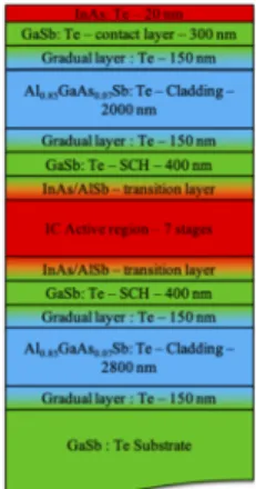
The epitaxial structure, displayed on Fig.1, consists of a separate confinement heterostructure (SCH) active region surrounded by (2.8-µm-thick bottom and 2-µm-thick top) Al0.85Ga0.15As0.07Sb0.93 cladding layers n-doped at 5.1017cm−3. This stack is inserted between the n-contact (300-nm GaSb/20-nm InAs) layers on the top side and a 100 nm-thick n-type graded (from GaSb to Al0.85Ga0.15As0.07Sb0.93) layer on the bottom side. The active gain region of the studied ICL structures comprises 7 QW/injectors stacked stages similarly to the design in [26], except for minor changes in the layer thickness of the layers to adjust the emission to the target wavelength of 3.3 µm. The layer sequence used here is as follows: 2.5 nm AlSb/1.5 nm InAs/ 3.0 nm Ga0.65In0.35Sb/1.4 nm InAs/1.0 nm AlSb/3.0 nm GaSb/ 1.0 nm AlSb/4.5 nm GaSb/2.5 nm AlSb/4.2 nm InAs/1.2 nm AlSb/3.2nm InAs/1.2nm AlSb/2.5nm InAs/1.2nm AlSb/ 2.0 nm InAs/1.2 nm AlSb/1.7 nm InAs/1.2 nm AlSb/1.5 nm InAs, where the four inner InAs layers of the electron injector are n-doped at 4.5 1018cm−3. This active region is inserted between 400-nm-thick GaSb layers slightly n-doped at 5.1016cm−3to reduce the free carrier optical losses [28]. The ICL wafers were grown by molecular beam epitaxy (MBE) in a RIBER Compact 21E solid source system equipped with As- and Sb- valved cracker cells. The growths were performed on 2-inch (100)-oriented n-type GaSb substrates. The growth temperature was monitored with a calibrated optical pyrometer on a GaSb substrate using the (1 × 3) to (2 × 5) surface reconstruction [27]. After thermal de-oxidation at 550°C under Sb flux, the temperature was ramped down to 500°C to grow the n-doped GaSb buffer and the lower cladding layer. During the growth of the bottom-SCH the substrate temperature was ramped down to 435°C for the growth of the active
region. Next, during the growth of the 400-nm-thick n-type GaSb upper-SCH, the temperature was ramped up to the temperature chosen for the top cladding quaternary layer. For this study, four different structures were grown with substrate growth temperatures of the top cladding layers respectively of 490°C, 475°C, 460°C and 435°C.
Fig. 1. Scheme of the ICL structure with two AlGaAsSb cladding layers.
The crystalline quality of the structures was assessed by high-resolution X-ray diffraction (HR-XRD) measurements using a PANalytical X’Pert3 MRD equipped with a PIXcel1D linear detector, an X-ray tube delivering the CuKα1 radiation and a four-bounce asymmetric Ge (2 2 0) monochromator. The experimental ω-2θ patterns measured on the (004) reflection for these four structures are shown on Fig.2together with the simulation of the intended ICL structures. The cladding layers are lattice matched except for the one grown at the lower temperature due to a lower As incorporation. The diffractograms of each sample exhibit a series of satellite peaks up to the 16thorder arising from the ICL active regions’ periodicity. The slight shift of the satellite peaks toward tensile strain when the top cladding layer temperature increases could be explained by the intermixing of the InSb bonds with respect of the AlAs bonds which are present at the interfaces.
The inset in Fig.2displays the full width half maximum (FWHM) averaged of the 10 satellite peaks closest to the substrate. The narrower satellite peaks are achieved for the samples grown at the lowest temperature which indicates more homogeneous interfaces within the interband cascade active region. The thickness of the ICL active region extracted from the angle separation between the satellite peaks is 41 nm for all the samples, in good agreement with the 41.5 nm target value.
To compare the lasing properties of the four structures, we fabricated broad-area 100-µm-wide ridge lasers. Ti-Au top-contact stripes were first deposited and served as a hard mask for the subsequent chlorine-based inductively coupled plasma reactive ion etching (ICP-RIE) of the mesas down to the bottom cladding layer. Then, the GaSb substrate backside is thinned down to 200 µm and coated with an Pd/AuGeNi back contact layer by sputtering deposition. The processed wafers were then cleaved to form 2-mm-long Fabry-Perot lasers that were mounted epi-side up onto a copper heatsink using indium solder. No passivation or insulation layers nor facet coatings were used.
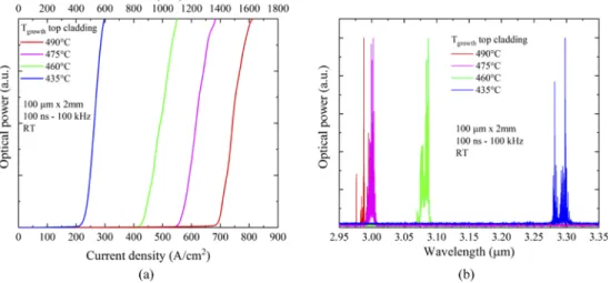
The four structures were characterized under pulsed electrical injection (100 ns pulses, 1 kHz repetition rate) at 25°C. The Fig.3(a) shows the typical light-current characteristics of these four ICLs, whereas Fig.3(b) displays the associated emission spectra (at I= 1.1 Ith). As suggested above, these data highlight a clear correlation between the laser performance and the growth temperature of the top cladding layers of the structures.
Fig. 2. ω-2θ HRXRD scans at the (0 0 4) reflection for the ICL structures with top cladding layers grown at different temperatures and simulation of the targeted ICL. Inset: Evolution of the average FWHM value of the satellite peaks versus the substrate growth temperature of the top cladding layers.
Fig. 3. Electro-optical properties of 100 µm x 2 mm ICLs with top cladding layers respectively grown at 490°C (red), 475°C (purple), 460°C (green) and 435°C (blue). (a) Laser emission spectra. (b) Light-current characteristics in pulsed injection regime.
For the laser whose top cladding layer was grown at the conventional AlGaAsSb substrate growth temperature of 490°C, the threshold current density Jthis 690 A/cm2and the laser emission wavelength is around 2.98 µm. We then observe a clear redshift of the emission wavelength and an improvement in the performance of the lasers as the upper cladding layer growth temperature decreases. When the latter is 435°C, the threshold current density decreases down to 220 A/cm2 while the emission wavelength shifts up to 3.3 µm, the target wavelength. This performance is comparable to the best threshold current densities obtained with state-of-the-art ICLs with a similar emission wavelength but based on the usual AlSb/InAs cladding layers (∼ 150-200 A/cm2) [6].
Figure4summarizes the evolution of the threshold current density and emission wavelength with the growth temperature of the top cladding layer. The threshold current density increases linearly with the growth temperature.
Fig. 4. Evolution of the threshold current density and emission wavelength with the growth temperature of the top cladding layer.
3. Impact of intermixing on wavelength emission
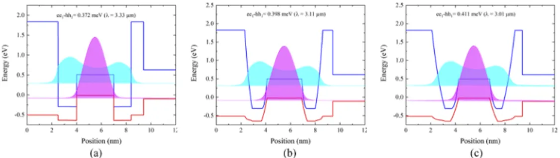
The performance degradation for the high temperatures is accompanied by a decrease in the emission wavelength that levels off at about 3 µm above 470°C. We attribute the latter observation to intermixing that occurs at the numerous InAs/AlSb and InAs/GaInSb interfaces of the active region. Such behavior has already been reported for “W” QWs active zones grown at different temperatures [29]. However, in the present case, we demonstrate that the growth temperature of the layers above the IC active region also affects the performance of the laser. We show in Figs.5the band diagram and the energy position of electron and whole levels of the “W” QWs calculated using the Nextnano software [30].
Fig. 5. Calculated band alignment and wavefunction of the type-II “W” AlSb/InAs/GaInSb/InAs/AlSb QW used in the ICL, without (a), with 0.5 nm (b) and 1 nm (c) broad intermixing at the interfaces.
In the structure with sharp interfaces, the transition energy corresponds to the emission wavelength of 3.3 µm. Assuming a 0.5 nm and 1-nm broadening of the interfaces [31] due to the intermixing leads to a shift of the quantum levels within the QWs that results in an emission wavelength of 3.11 µm and 3 µm, respectively. This is consistent with the data measured in the
lasers whose top cladding layer was grown at high temperature. In addition, we believe that intermixing also affects the injector regions thus modifying their band structure, which results in decreasing injection efficiency and high threshold current density. This effect is probably also combined with the observation that threshold current density increases in ICL at shorter wavelength [6].
4. ICL performance analysis
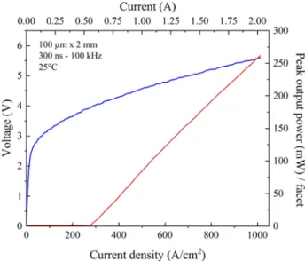
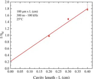
The epitaxial structure with the top cladding grown at a substrate temperature of 435°C was cleaved to form 2-mm-, 3-mm- and 4-mm-long cavities which were then characterized to determine the internal quantum efficiency (ηi) and internal losses (αi). The measurements were performed in pulsed regime (300 ns/100 kHz) at 25°C. The optical power was measured with a powermeter placed in front of the ICL in order to maximize the collected output light. Figure6
presents typical characteristics of the 2-mm-long lasers. The I-V curve shows a threshold voltage of 3.8 V which exceeds the theoretical value by only 1.2 V corresponding to a high voltage efficiency of 68%. The series resistance is in the range of 1-2 ohms, comparable with published results on ICLs emitting in the same wavelength range [12,13,17].
Fig. 6. Pulsed (300 ns/100 KHz) light-current-voltage characteristic of a 2-mm-long 100-µm-wide laser at 25°C.
The reciprocal differential external quantum efficiency (ηd) is shown in Fig.7as a function of the laser length. From the well-known relation ηd= ηi/[1+ αiL/ln(1/R)], where L is the cavity length and R is the facet reflectivity (R= 0.31), the value of ηiand αiare extracted to be 65% per stage and 15 cm−1, respectively. The η
ivalue is close to those reported for ICLs with AlSb/InAs claddings whereas αiis higher than the values typically measured on ICLs [26,32]. The origin of this high internal loss is not well understood and could be due to a stronger absorption in the n-type Al0.85Ga0.15As0.06Sb0.94cladding layers than in devices with superlattice claddings. Indeed, the Te-doped AlSb presents a strong absorption between 3 and 4 µm since Te is considered to act as a shallow donor [33,34]. A thicker GaSb SCH layer could be employed to reduce the overlap between the optical mode and the cladding layers and thus to decrease the waveguide loss [12,35]. This excess losses could also arise from the oxidation of the laser sidewall which are not protected in our process.
Fig. 7. Reciprocal differential quantum efficiency versus the cavity length in pulsed regime (300 ns/100 kHz) at 25°C. Each datapoint represents averaged measurements from several devices (4-5) except for the 4 mm cavity length which only features the 2 best results.
5. Ridge ICL processing and performance
To achieve CW operation and to perform a more application-relevant assessment of the laser performance, narrow ridge lasers were fabricated using the laser structure with the lower top cladding temperature using the following process flow. First, ridges of different widths between 5 and 10 µm were patterned using an SPR700 photoresist. The mesas were subsequently dry etched using ICP-RIE technique with a BCl3-Cl2-Ar chemistry down to the middle of the bottom SCH layer to avoid the oxidation of the bottom AlGaAsSb cladding layer before dielectric layer deposition. The ridges were then encapsulated using a Si3N4/SiO2bi-layer deposited by ICP-PECVD. Window openings in these top insulating layers to enable the deposition of Ti:Au top contacts were made using an additional lithographic step and a CF4-based ICP-RIE etching. As for the broad-area lasers, the GaSb substrate was thinned and coated with an Pd/AuGeNi back contact. The processed wafer was, then cleaved and a set of laser chips were mounted epi-side down on a copper heatsink for electro-optical characterization. Optical facets were left untreated.
Figure8shows the L-I-V curve of a 7 µm x 2 mm ridge laser. CW operation was achieved with this device up to a heat sink temperature as high as 80°C. The maximum output power could not be measured for mount temperatures lower than 60°C because our power supply was limited to 8V and the thermal roll-over was not reached, but it exceeds 12 mW/uncoated facet and 10 mW at 20°C and 40°C, respectively. About 1 mW/uncoated facet was still measured at 80 °C (Fig.8). The I-V curve exhibits a turn voltage of 4 V and a serial resistance of 5 W. In comparison with the above-reported broad area ICLs, this lower performance is attributed to the etching of the InAs top contact layer during the process and the fact that Ti:Au contacts on n-doped GaSb tend to lead to Schottky contacts [36] which, in turn, increase the turn-on voltage and series resistance. Nevertheless, the threshold current was as low as 40 mA at 20°C, equivalent to 286 A/cm2, slightly higher that the pulsed value measured for the broad-area lasers, an expected degradation imposed by the excess ridge-roughness-related losses and the increased thermal load. Between 20°C and 80°C, the temperature dependence of the threshold current gives a characteristic temperature T0= 50 K up to 65°C and 25 K between 65°C and 80°C. This value is comparable to that of ICLs with AlSb/InAs cladding layers [12].
Fig. 8. CW light-current-voltage curves at different temperatures between 20°C and 80°C from a 7 µm ridge width and 2 mm long cavity ICL with AlGaAsSb cladding layers.
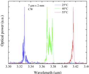
Finally, Fig.9shows the emission spectra of this laser measured at 25°C, 40°C and 55°C. The spectra reveals multimode operation and a peak emission wavelength increasing from 3.33 µm at 25°C to 3.41 µm at 55°C with a rate of about 2.6 nm/K, a value adapted to gas spectroscopy.
Fig. 9. CW laser emission spectra taken at 150 mA at different temperatures (25°C, 40°C and 55°C).
6. Conclusion
In this paper, we have reported ICLs employing AlGaAsSb bulk cladding layers instead of the commonly used InAs/AlSb superlattice claddings. We have demonstrated the positive effect of low growth temperature for the upper cladding quaternary layer on the ICL performance. When the top cladding layer is grown at a temperature exceeding the growth temperature of the active region, a significant increase of the threshold current densities is observed whereas the emission wavelength is blue-shifted. This variation is attributed to the intermixing that occurs at the numerous interfaces within the active region during the growth of the top cladding layer.
For the optimized ICLs a threshold current density as low as 220 A/cm2was obtained for broad area lasers in pulsed regime. The lasers exhibit internal quantum efficiency of 65% per active stage. The internal loss was found to be 15 cm−1and could be attributed to the absorption in the Te-doped AlGaAsSb layer and sidewall oxidation. CW operation near 3.35 µm has been achieved for narrow stripe 7-µm-wide lasers mounted epi-side down up to a temperature of 80°C without facet coating. This work shows that AlGaAsSb cladding layers grown under optimized conditions can be successfully used to fabricate high performance ICLs.
Funding
Agence Nationale de la Recherche (ANR-11-EQPX-0016, ANR-16-CE24-0011). Acknowledgement
This work partially benefited from support of the French RENATECH network and its LAAS-CNRS technological facility.
References
1. A. Soibel, M. W. Wright, W. H. Farr, S. A. Keo, C. J. Hill, R. Q. Yang, and H. C. Liu, “Midinfrared Interband cascade Laser for Free Space Communication,”IEEE Photonics Technol. Lett.22(2), 121–123 (2010).
2. M. Jahjah, A. Vicet, and Y. Rouillard, “A QEPAS based methane sensor with a 2.35 µm antimonide laser,”Appl. Phys. B: Lasers Opt.106(2), 483–489 (2012).
3. M. Dagan, B. Thomas, B. Gross, and F. Moshary, “Implementation of micropulse LIDAR at 4.5 µm and 1.55 µm for aerosol and cloud study,” in Proceedings of 27th International Laser Radar Conference, 119, (EPJ Web of Conferences, 2016), UNSP 06001.
4. R. Ghorbani and F. M. Schmidt, “ICL-based TDLAS sensor for real-time breath gas analysis of carbon monoxide isotopes,”Opt. Express25(11), 12743 (2017).
5. R. Q. Yang, “Infrared laser based on intersubband transitions in quantum wells,”Superlattices Microstruct.17(1),
77–83 (1995).
6. I. Vurgaftman, R. Weih, M. Kamp, J. R. Meyer, C. L. Canedy, C. S. Kim, M. Kim, W. W. Bewley, C. D. Merritt, J. Abell, and S. Höfling, “Interband cascade lasers,”J. Phys. D: Appl. Phys.48(12), 123001 (2015).
7. M. Razeghi, “High-performance InP based mid-IR Quantum Cascade Laser,”IEEE J. Sel. Top. Quantum Electron.
15(3), 941–951 (2009).
8. Y. Yao, A. J. Hoffman, and C. Gmachl, “Mid-Infrared quantum cascade lasers,”Nat. Photonics6(7), 432–439 (2012).
9. A. Sahli, Y. Rouillard, J. Angellier, and M. Garcia, “Very-low-threshold 2.4-µm GaInAsSb-AlGaAsSb laser diodes operating at room temperature in the continuous-wave regime,”IEEE Photonics Technol. Lett.16(11), 2424–2426
(2004).
10. L. Shterengas, G. Belenky, G. Kipshidze, and T. Hososda, “Room temperature operated 3.1 µm type-I GaSb-based diode lasers with 80 mW continuous-wave output power,”Appl. Phys. Lett.92(17), 171111 (2008).
11. C. S. Kim, M. Kim, J. Abell, W. W. Bewley, C. D. Merritt, C. L. Canedy, I. Vurgaftman, and J. R. Meyer, “Mid-infrared distributed-feedback interband cascade lasers with continuous-wave single-mode emission to 80°C,”Appl. Phys. Lett.101(6), 061104 (2012).
12. R. Weih, M. Kamp, and S. Höfling, “Interband cascade lasers with room temperature threshold current densities below 100 A/cm2,”Appl. Phys. Lett.102(23), 231123 (2013).
13. C. L. Canedy, J. Abell, C. D. Merritt, W. W. Bewley, C. S. Kim, M. Kim, I. Vurgaftman, and J. R. Meyer, “Pulsed and CW performance of 7-stage interband cascade lasers,”Opt. Express22(7), 7702–7710 (2014).
14. J. R. Meyer, C. A. Hoffman, F. J. Bartoli, and L. R. RamMohan, “Type-II quantum-well lasers for the mid-wavelength infrared,”Appl. Phys. Lett.67(6), 757–759 (1995).
15. I. Vurgaftman, W. W. Bewley, C. L. Canedy, C. S. Kim, M. Kim, J. R. Lindle, C. D. Merritt, J. Abell, and J. R. Meyer, “Mid-IR type-II interband cascade lasers,”IEEE J. Sel. Top. Quantum Electron.17(5), 1435–1444 (2011).
16. S. Roux, P. Barritault, O. Lartigue, L. Cerutti, E. Tournié, B. Gérard, and A. Grisard, “Mid-Infrared characterization of refractive indices and propagation losses in GaSb/AlXGa1-XAsSb waveguides,”Appl. Phys. Lett.107(17), 171901
(2015).
17. R. Weih, A. Bauer, M. Kamp, and S. Höfling, “Interband cascade lasers with AlGaAsSb bulk cladding layers,”Opt. Mater. Express3(10), 1624–1631 (2013).
18. T. Borca-Tasciuc, D. W. Song, J. R. Meyer, I. Vurgaftman, M. J. Yang, B. Z. Nosho, L. J. Whitman, H. Lee, R. U. Martinelli, G. W. Turner, M. J. Manfra, and G. Shen, “Thermal conductivity of AlAs0.07Sb0.93 and Al0.9Ga0.1As0.07Sb0.93alloys and (AlAs)1/(AlSb)11digital-alloy superlattices,”J. Appl. Phys.92(9), 4994–4998 (2002).
19. C. Zhou, B. Cui, C. L. Canedy, C. S. Kim, M. Kim, W. W. Bewley, C. D. Merritt, J. Abell, J. R. Meyer, and M. Grayson, “Thermal conductivity tensors of the cladding and active layers of interband cascade lasers,”Appl. Phys. Lett.105(26), 261905 (2014).
20. A. Bauer, M. Dallner, A. Herrmann, T. Lehnhardt, M. Kamp, S. Höfling, L. Worschech, and A. Forchel, “Atomic scale interface engineering for strain compensated epitaxially grown InAs/AlSb superlattices,”Nanotechnology
21(45), 455603 (2010).
21. T. Hosoda, G. Kipshidze, G. Tsvid, L. Shterengas, and G. Belenky, “Type-I GaSb-based laser diodes operating in 3.1-to 3.3 µm wavelength range,”IEEE Photonics Technol. Lett.22(10), 718–720 (2010).
22. K. Vizbaras and M. C. Amann, “Room temperature 3.73 µm GaSb-based type-I quantum-well lasers with quinternary barriers,”Semicond. Sci. Technol.27(3), 032001 (2012).
23. L. Cerutti, A. Castellano, J. B. Rodriguez, L. Largeau, A. Balocchi, K. Madiomanana, F. Lelarge, G. Patriarche, X. Marie, and E. Tournié, “GaSb-based composite quantum wells for laser diodes operating in the telecom wavelength range near 1.55 µm,”Appl. Phys. Lett.106(10), 101102 (2015).
24. S. Simanowsky, M. Walther, J. Schmitz, R. Kiefer, N. Herres, F. Fuchs, M. Maier, C. Mermelstein, J. Wagner, and G. Weimann, “Arsenic incorporation in molecular beam epitaxy (MBE) layers 2.0-2.5 µm laser structures on GaSb substrates,”J. Cryst. Growth201-202, 849–853 (1999).
25. C. L. Canedy, J. Abell, W. W. Bewley, E. H. Aifer, C. S. Kim, J. A. Nolde, M. Kim, J. G. Tisher, J. R. Lindle, E. M. Jackson, I. Vurgaftman, and J. R. Meyer, “Molecular beam epitaxial growth effects on type-II antimonide lasers and photodiodes,”J. Vac. Sci. Technol., B28(3), C3G8–C3G12 (2010).
26. I. Vurgaftman, W. W. Bewley, C. L. Canedy, C. S. Kim, M. Kim, C. D. Meritt, J. Abell, J. R. Lindle, and J. R. Meyer, “Rebalancing of internally generated carriers for mid-infrared interband cascade lasers with very low power consumption,”Nat. Commun.2(1), 585 (2011).
27. A. S. Bracker, M. J. Yang, B. R. Bennett, J. C. Culbertson, and W. J. Moore, “Surface reconstruction phase diagrams for InAs, AlSb, and GaSb,”J. Cryst. Growth220(4), 384–392 (2000).
28. S. Roux, L. Cerutti, E. Tournié, B. Gérard, G. Patriarche, A. Grisard, and E. Lallier, “Low-loss orientation-patterned GaSb waveguides for mid-infrared parametric conversion,”Opt. Mater. Express7(8), 3011–3016 (2017).
29. M. J. Yang, W. J. Moore, B. R. Benett, B. V. Shanabrook, J. O. Cross, W. W. Bewley, C. L. Felix, I. Vurgaftman, and J. R. Meyer, “Optimum growth parameters for type-II infrared lasers,”J. Appl. Phys.86(4), 1796–1799 (1999).
30. Seewww.nextnano.com/index.phpfor “Nextnano GmbH - semiconductor software solutions.”
31. W. Barvosa-carter, M. E. Twigg, M. J. Yang, and L. J. Whitman, “Microscopic characterization of InAs/In0.28Ga0.72Sb/InAs/AlSb laser structure interfaces,”Phys. Rev. B63(24), 245311 (2001).
32. C. D. Merritt, W. W. Bewley, C. S. Kim, C. L. Canedy, I. Vurgaftman, J. R. Meyer, and M. Kim, “Gain and loss as a function of current density and temperature in interband cascade lasers,”Appl. Opt.54(31), F1–F7 (2015).
33. W. J. Turner and W. E. Reese, “Infrared Absorption in n-Type Aluminum Antimonide,”Phys. Rev.117(4), 1003–1004
(1960).
34. W. Jost, M. Kunzer, and U. Kaufmann, “Bistability of the Te donor in AlSb: Te bulk crystals,”Phys. Rev. B50(7),
4341–4344 (1994).
35. M. Kim, W. W. Bewley, C. L. Canedy, C. S. Kim, C. D. Merritt, J. Abell, I. Vurgaftman, and J. R. Meyer, “High-power continuous-wave interband cascade lasers with 10 actives stages,”Opt. Express23(8), 9664–9672 (2015).
36. A. Subekti, V. W. L. Chin, and T. L. Tansley, “Ohmic contacts to n-type and p-type GaSb,”Solid-State Electron.