HAL Id: hal-03033135
https://hal.univ-lorraine.fr/hal-03033135
Submitted on 3 Dec 2020HAL is a multi-disciplinary open access archive for the deposit and dissemination of sci-entific research documents, whether they are pub-lished or not. The documents may come from teaching and research institutions in France or abroad, or from public or private research centers.
L’archive ouverte pluridisciplinaire HAL, est destinée au dépôt et à la diffusion de documents scientifiques de niveau recherche, publiés ou non, émanant des établissements d’enseignement et de recherche français ou étrangers, des laboratoires publics ou privés.
Electrochemically Assisted Deposition of Nanoporous
Silica Membranes on Gold Electrodes: Effect of
3-Mercaptopropyl(trimethoxysilane) “Molecular Glue”
on Film Formation, Permeability and Metal
Underpotential Deposition
Wahid Ullah, Grégoire Herzog, Neus Vilà, Mariela Brites Helú, Alain
Walcarius
To cite this version:
Wahid Ullah, Grégoire Herzog, Neus Vilà, Mariela Brites Helú, Alain Walcarius. Electrochem-ically Assisted Deposition of Nanoporous Silica Membranes on Gold Electrodes: Effect of 3-Mercaptopropyl(trimethoxysilane) “Molecular Glue” on Film Formation, Permeability and Metal Un-derpotential Deposition. ChemElectroChem, Weinheim : Wiley-VCH, 2020, �10.1002/celc.202001347�. �hal-03033135�
Electro-assisted deposition of nanoporous
silica membranes on gold electrodes:
effect of
3-mercaptopropyl(trimethoxysilane)
“molecular glue” on film formation,
permeability and metal underpotential
deposition
Wahid Ullah,
[a]Grégoire Herzog,
[a]* Neus Vilà,
[a]Mariela
Brites-Helú,
[a]Alain Walcarius
[a]*
[a] Université de Lorraine, CNRS, LCPME, Nancy, France
E-mail: gregoire.herzog@univ-lorraine.fr,
alain.walcarius@univ-lorraine.fr
Abstract: Gold electrodes have been covered with vertically aligned mesoporous silica thin films by electro-assisted self-assembly. To ensure uniform surface coverage and good adhesion of the membrane to the gold surface, it was necessary to use a (3-mercaptopropyl)trimethoxysilane (MPTMS) reagent acting as “molecular glue” thanks to its thiol function able to bind to the gold substrate and to its alkoxysilane moieties enabling condensation with the silica material. The MPTMS layer had however significant effect on film permeability to redox species (Ru(NH3)63+ and ferrocenedimethanol (Fc(MeOH)2)). MPTMS adsorption should be long enough to ensure proper adhesion of the film but not too long to avoid surface blocking or film defects; an optimal time window of 60-600 s soaking in 0.1 mM MPTMS in ethanol was evidenced. In addition, Cu underpotential deposition (UPD) experiments revealed that the silica membrane affected significantly the UPD process, suggesting some barrier effect of the porous membrane, but the interface Au/MPTMS/silica is not sharp and allowed metal UPD between the gold substrate and the silica thin film.
Introduction
A single metal monolayer deposited on a foreign metal surface is of interest for a range of applications: electrocatalysis,[1] mercury-free metal sensing,[2,3] and preparation of nanostructures.[4-9] Such metal deposits, known as underpotential deposits, occur at a potential higher than the one predicted by Nernst equation.[10] Cu underpotential deposition on gold electrode is one of the most studied systems and was selected here as a model system to investigate underpotential deposition through mesoporous silica films as templates. Recently, Cu was underpotentially deposited through an anodized aluminium oxide to form
nanostructured electrodes for various applications.[11] Indeed, nanostructured electrode surfaces have become an intense research area, with appealing applications in various fields such as: electroanalysis and sensors,[12-15] biosensors or immunosensors and biofuel cells, [16-20] energy conversion and storage,[21-24] electrocatalysis,[25,26] or electrochemical actuators.[27]
Nanostructures can be generated electrochemically[12,28,29] and the use of either hard or soft templates enables the formation of highly ordered porous films on electrodes.[30,31] An interesting configuration is offered by porous membranes made of nanopores orthogonally oriented to the electrode surface, as they ensure fast transport from the solution to the electrode surface or can be used to generate ensembles of ordered nanotubules or nanofibers, thanks to the vertical alignment of 1D nanochannels.[32-35] Modified electrodes of that type can be easily elaborated from track-etched polycarbonate membranes or nanoporous anodic aluminum oxides, but they are often restricted in terms of pore diameters (> 10 nm).[36] A way to overcome this limitation is provided by some reported methods for the preparation of mesoporous silica films exhibiting a high density of hexagonally packed nanochannels that are vertically aligned with respect to the underlying support.[37-39] In our group, we have developed the electrochemically assisted self-assembly (EASA) of oriented mesoporous silica membranes on various electrode surfaces.[37] In doing so, one can get vertically ordered silica mesochannel films with small pore diameter (2-3 nm), high packing density (>1012 pores per cm2) and mesochannel lengths typically in the 50-100 nm range.[37,40] These films are mechanically stable and well-adherent when grown onto oxide-based electrode surfaces likely to form covalent bonds with silica, but they may require the use of an additional adhesive layer to ensure strong attachment to other electrode materials (such as carbon, for instance).[41] They exhibit molecular sieving properties at the nanoscale, demonstrating the very good quality of uniformly-packed nanopores over wide area crack-free films.[42] They appear thus as almost ideal mask to define arrays of nanodisk electrode ensembles.
Here we have prepared vertically aligned mesoporous silica thin films by EASA on gold electrodes which were pre-treated with a thiol-containing silane reagent (i.e., (3-mercaptopropyl)-trimethoxysilane, MPTMS) likely to act as gluing agent between the gold surface and the silica material. MPTMS is indeed known to be a good molecular adhesive between glass and gold surfaces.[43] Compared to our previous works,[37,40-42] this is the first attempt to get EASA films on gold with the silica membrane adhering well to the electrode surface. We investigated here the effect of this molecular glue on film formation and its permeability to redox probes Ru(NH3)63+ and Fc(MeOH)2), by optimizing its surface coverage. Copper UPD was then performed in potentiostatic and potentiodynamic modes on both bare and modified electrodes, respectively before and after removing the surfactant template to characterize the interface formed by the MPTMS between the porous film and the gold surface.
Results and Discussion
Electro-assisted self-assembly of mesoporous silica film on gold using MPTMS
as molecular glue and effect of permeability to redox probes
Mesoporous silica films generated by EASA exhibit good adhesion to oxide-based electrodes (such as ITO or FTO) thanks to the reaction of their surface hydroxyl groups with silica,[40,44] but may require an electrode surface pretreatment step in other cases.[41,45,46] Dealing with gold electrode, the direct deposition of mesoporous silica by EASA led to non-uniformly deposited film which may even peel off from the electrode surface (Fig. S1A). A way to circumvent this
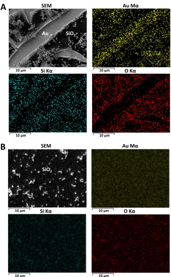
drawback would be the use of a reagent such as MPTMS, which is expected to bind to gold surfaces by chemisorption via its thiol function and to condensate with silica precursors via its alkoxysilane moieties.[47] The effectiveness of this approach is demonstrated from SEM examination of a silica film prepared by EASA using a gold electrode previously soaked in MPTMS medium, showing that a uniform crack-free deposit (with some aggregates, as common for EASA films[40]) over the whole electrode surface can be obtained (Fig. S1B). Such film is kept intact after attempting to remove it with a scotch tape, confirming the real molecular glue effect of MPTMS in ensuring good adhesion of silica onto the gold surface (even if some reductive desorption of MPTMS can occur, this process does not remove completely the adsorbed MPTMS[48]). High magnification SEM views combined to Energy Dispersive Analysis of X-rays (EDX) confirm the uniform silica coating on the whole MPTMS-treated gold whereas incomplete coverage of gold is shown through enhanced contributions of Au signal and concomitant decrease of Si and O signals (Fig. 1A, contrary to the uniform and less intense Au Mα image when the silica film is covering the whole gold surface (Fig. 1B)). Note that non-covered and film-coated Au surfaces can be distinguished even if the analysis depth of EDX extends from the silica membrane, the gold film and some part of the underlying glass support, via contrast changes on the EDX mapping images (Fig. 1A) whereas no contrast changes can be noticed on the film uniformly covering the whole gold surface (Fig. 1B). The white dots on the SEM micrograph (top left of Fig. 1B) correspond to the silica particles/aggregates located on top of the mesoporous layer (which are also visible on the silica portions of the deposits made without MPTMS, see top left of Fig. 1A).
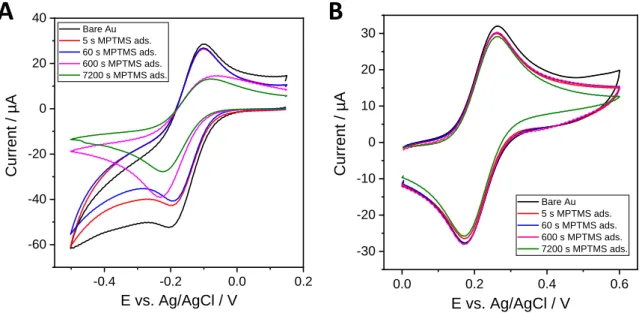
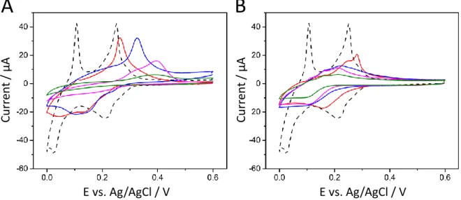
Notwithstanding the beneficial role of the MPTMS layer on the adhesion properties of the silica film, it can also affect either the response to redox probes or the structural and morphological features of the mesoporous membrane generated by EASA. Figure 2 shows the voltammetric response of Ru(NH3)63+ and ferrocenedimethanol (Fc(MeOH)2) species using gold electrodes treated for various times in MPTMS (which is likely to form self-assembled monolayers of different packing and even thicker deposits[49]).The partial and progressive coverage of the gold electrode surface with MPTMS is evidenced when using Ru(NH3)63+ as redox probe in solution (Fig. 2A). A decrease in the current response in comparison to the bare electrode is as more marked with lengthening the MPTMS adsorption time, with slightly larger anodic-to-cathodic peaks separation (from 95 to 160 mV) for longer times (600 and 7200 s), indicating slower electron transfer rates, consistent with previous observations.[48] More limited effects were however observed at shorted times (i.e., 20 & 23% decrease in peak current intensities, respectively for 5 & 60 s adsorption) thanks to the rather low packing density of the MPTMS layer. On the other hand, using the neutral Fc(MeOH)2 probe resulted in almost the same current responses (Fig. 2B), suggesting fast transfer processes independently on the presence of the MPTMS layer.
Figure 1. SEM micrographs and EDX mapping (Au, Si and O elements) of mesoporous silica thin films
deposited by EASA on (A) bare Au electrode or (B) MPTMS-treated Au electrode (1 min in 0.1 mM MPTMS in ethanol).
Si Kα
O Kα
10 µm 10 µmAu Mα
SEM
Au SiO
2Au Mα
SEM
SiO
2 10 µm 10 µmSi Kα
O Kα
10 µm 10 µm 10 µm 10 µmA
B
Figure 2. CV curves recorded at 100 mV s-1 in (A) 0.5 mM Ru(NH3)63+ (+ 0.1 M KCl) or (B) 0.5 mM
Fc(MeOH)2 (+ 0.1 M NaNO3), using bare Au electrode or MPTMS-treated Au electrode (in 0.1 mM
MPTMS in ethanol, respectively for 5, 60, 600 and 7200 s).
The effective exposure to the gold surface is consistent with XPS data indicating always a major contribution of Au 4f signal independently of the amount of MPTMS (Table S1). A possible explanation of the difference between the two probes is the fact that Fc(MeOH)2 is not expected to interact with the MPTMS layer while Ru(NH3)63+ species are likely to be involved in electrostatic interactions with the silanolate groups originating from hydrolyzed methoxysilane bonds in aqueous medium (given pKa values of silanol/silanolate groups around 6.8±0.2[50] and the isoelectric point of silica at pH 2-3,[51] the surface is thus negatively charged in the conditions used here). The electrostatic effects are also pointed out when using a negatively charged redox probe (Fe(CN)64-) for which large overpotentials and peak vanishing are observed (Fig. S2), in agreement with literature.[49]
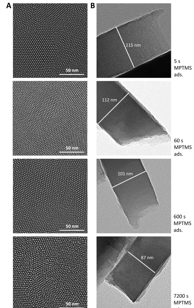
Another important question, in addition to the proper adhesion of the mesoporous silica film thanks to the MPTMS layer, is how it would affect (or not) the film growth by EASA in terms of thickness, structural morphology (i.e. nanochannel orientation, pore size and geometry) and permeability. Analysis of the films obtained on the various MPTMS-treated electrodes by transmission electron microscopy (TEM, Fig. 3) confirms a compact hexagonal packing of the pores (see top views on Fig. 3A) with linear mesochannels oriented perpendicularly to the underlying substrate (see cross section views on Fig. 3B), yet perhaps with more grain boundaries and/or small defects on electrodes treated with MPTMS for longer times (especially 7200 s). The mesopores diameter is 2.4 nm, with a pore-to-pore distance of 4.0 nm, so that the electrode surface at the bottom of the pores accessible to the species in solution represented approximately 35 % of the geometric surface area of the electrode. For a given sample, the film thickness is uniform. However, the film thickness decreases (from 115 to 87 nm) when the duration of MPTMS treatment increased, which can be related to increasing amounts of molecular glue slowing down the EASA process by more resistance to mass and charge transfer in agreement with observations made above by CV (Fig. 2). These results reflect that the presence of MPTMS molecules does not alter the vertical growth of the mesostructured silica membrane including pore size and hexagonal geometry, yet with some effect on film thickness and possibly more defects or less mesostructural order for the films
0.0 0.2 0.4 0.6 -30 -20 -10 0 10 20 30 Cu rrent / µA E vs. Ag/AgCl / V Bare Au 5 s MPTMS ads. 60 s MPTMS ads. 600 s MPTMS ads. 7200 s MPTMS ads. -0.4 -0.2 0.0 0.2 -60 -40 -20 0 20 40 Cu rrent / µA E vs. Ag/AgCl / V Bare Au 5 s MPTMS ads. 60 s MPTMS ads. 600 s MPTMS ads. 7200 s MPTMS ads.
A
B
prepared from Au electrodes treated with MPTMS for longer times. The reproducibility of the film preparation procedure is very satisfactory (less than 5% variation in thickness and always the same hexagonal packing and orientation of mesopores) but the mesostructure suffers from poor storage stability of the thin silica gel walls in the atmosphere (ca. some days after surfactant removal and one month with CTAB kept in the film), as common for such materials.
Figure 3. TEM micrographs of mesoporous silica films generated on Au electrodes treated with MPTMS
for 5, 60, 600 and 7200 s (from top to bottom): (A) top views and (B) cross sections.
115 nm 112 nm 101 nm 87 nm 50 nm 50 nm 50 nm 50 nm
A
B
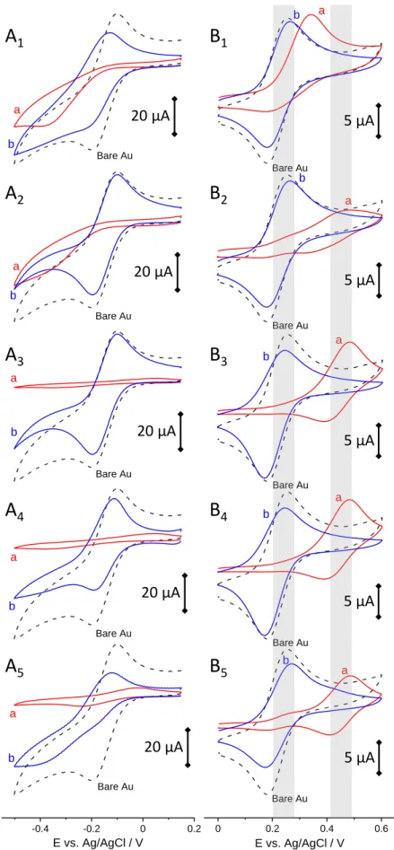
5 s MPTMS ads. 60 s MPTMS ads. 600 s MPTMS ads. 7200 s MPTMS ads.The various mesoporous silica films are investigated by cyclic voltammetry (CV) using the same redox probes as above (Ru(NH3)63+, see Fig. 4A, and Fc(MeOH)2, see Fig. 4B), respectively before (curves “a” in red) and after surfactant removal (curves “b” in blue). When using Ru(NH3)63+ probe to analyze the films prior to surfactant removal, negligible current responses are observed for Au-MPTMS-Silica electrodes prepared from 60 s and 600 s MPTMS adsorption (Fig. 4A3 & 4A4), revealing a defect-free and uniform membrane covering the whole electrode surface (because such probe is not likely to cross the hydrophobic surfactant barrier[40,41]). On the contrary, the MPTMS-free Au electrode covered with the mesoporous silica film results in a significant current (Fig. 4A1) indicating easy access of the probe to the electrode surface due to partial coverage (Fig. 1A), with electron transfer processes governed by diffusion of the probe through pinholes (charge transfer occurring on the gold free sites).[52] The Au-MPTMS-Silica electrode prepared from 5 s MPTMS adsorption also behaves similarly, yet with less intense currents (Fig. 4A2), suggesting that such short contact time improves film attachment but not enough to ensure complete blocking. Finally, a weak current wave appears for the 7200 s sample (Fig. 4A5), indicating the presence of some defects in the mesoporous film. After removal of the surfactant, the voltammetric peaks are restored to significant extents (see curves “b” in Fig. 4A), yet with more limitation for Au-MPTMS-Silica electrodes prepared from 600 s and especially 7200 s MPTMS adsorption, consistent with the partial blocking arising from a denser MPTMS layer (Fig. 2A).[48,49]
Confirmation and complementary information can be obtained when using ferrocenedimethanol (Fc(MeOH)2) as redox probe (Fig. 4B) for which one can distinguish two anodic currents (see greyed regions on parts B1-5 the Figure), one at 0.25 V (and corresponding cathodic peak at 0.18 V) due to solution-phase species and one at 0.48 V corresponding to the oxidation of Fc(MeOH)2 solubilized in the surfactant phase.[37,40] As shown, only Au-MPTMS-Silica electrodes prepared from 60 s and 600 s MPTMS adsorption gives rise to a single peak at 0.48 V prior to template extraction (see curves “a” in Fig. 4B3 & 4B4) and an intense couple of peaks at 0.25-0.18 V arising from fast diffusion of Fc(MeOH)2 species through the mesopore channels after surfactant removal (see curves “b” in Fig. 4B3 & 4B4), indicating the good quality of the oriented silica membranes. On these curves, one can also notice cathodic-to-anodic peak current ratios slightly larger than unity, due to some accumulation of ferrocenium cations via favorable electrostatic interactions with the negatively charged silica walls.[37] The fact that CVs (after template removal) are very close to that of a bare Au electrode, although the theoretical Au coverage is 0.35 (Au surface accessible to electrolyte), is explained by the very small pores (2.4 nm in diameter) located very close to each other (4.0 nm-to-center), so that the CV curves obey to a total overlap diffusion regime.[53] This concept of theoretical surface coverage will be more important when discussing the response of surface-confined processes such as Cu UPD (see next section thereafter).For other cases, small currents are observed in the 0.25 V region prior to surfactant removal (Fig. 4B2 & 4B5), indicating imperfect quality of the films and/or incomplete coverage, which is even more dramatic (larger currents) for the film electrode generated on MPTMS-free gold (Fig. 4B1) covering only partially the electrode surface, as suggested by microscopic observations. After surfactant removal, typical peak currents of solution-phase Fc(MeOH)2 species are restored (see curves “b” in Fig. 4B) due to the fast diffusion of (Fc(MeOH)2) through the vertical nanochannels,[37] except for the film prepared after 7200 s MPTMS adsorption for which the smaller peak intensity (Fig. 4B5) is explained by restricted diffusion through a probably less well-organized membrane (or containing some defects), as aforementioned for the Ru(NH3)63+ probe (Fig. 4A5).
Figure 4. CV curves recorded in 0.5 mM Ru(NH3)63+ (+ 0.1 M KCl) at 100 mV
s-1 (A) or in 0.5 mM Fc(MeOH)2 (+ 0.1 M NaNO3) at 20 mV s-1 (B), using MPTMS-free Au electrode (A
1,
B1) or MPTMS-treated Au electrodes (in 0.1 mM MPTMS in ethanol, respectively for 5 (A2, B2), 60 (A3,
B3), 600 (A4, B4) and 7200 s (A5, B5)), all covered with mesoporous silica films generated by EASA,
Bare Au a b Bare Au a b Bare Au a b Bare Au a b -0.4 -0.2 0 0.2 E vs. Ag/AgCl / V Bare Au a b Bare Au a b Bare Au a b Bare Au a b Bare Au a b 0 0.2 0.4 0.6 E vs. Ag/AgCl / V Bare Au a b
A
1B
1A
2B
2A
3B
3A
4B
4A
5B
520 µA
5 µA
20 µA
20 µA
20 µA
20 µA
5 µA
5 µA
5 µA
5 µA
respectively before (a, red curves) and after surfactant removal (b, blue curves); the CVs obtained on bare Au electrode have been added for comparison purpose (dashed black curves).
Both full coverage of the electrode surface with the film and effective surfactant removal are demonstrated by XPS (Fig. S3). The narrow XPS spectra corresponding to the Au 4f core-level (Fig. S3A), with single contributions of Au 4f 7/2 at 84.1 eV and Au 4f 5/2 at 87.8 eV corresponding to metallic Au0 with no trace of oxidation,[54] clearly indicate that the mesoporous silica material covers totally the gold surface as no gold contribution can be noticed upon film formation (curve “c”, repeated 5 times at different places of the sample). Also, the small difference observed after MPTMS adsorption (ca. 20% decrease with respect to bare Au, compare curves “a” and “b” in Fig. S3A) ascertains that the molecular glue used for film adhesion does not form a densely-packed layer, consistent with the above permeability data (Figs. 2 & Fig. 4). The high-resolution N 1s core-level spectra further confirms successful removal of the surfactant template, via the vanishing of the signal relative to quaternary ammonium moieties at 401 eV (Fig. S3B). Finally, one has to mention that no Au 4f signal can be observed after surfactant removal, although this leads to free Au surfaces at the bottom of mesopore channels, most probably due to shadowing effects arising from long (between 87 and 115 nm, depending on the MPTMS treatment duration) nanochannels which are not always perfectly linear over their whole length (Fig. 3B) leading to inelastic mean free path of electrons shorted than the silica membrane thickness.
One can summarize the conclusions of this first part as follows. SEM/EDX analysis of the modified electrode surface showed that, in the absence of a MPTMS pre-treatment, the silica membrane did not adhere to the gold substrate (Fig. 1A). Those SEM observations were confirmed by cyclic voltammetry of two redox probes, with currents indicating that an important portion of the electrode remained unmodified despite silica membrane deposition (Fig. 4A1&B1). A MPTMS treatment was used to improve the adhesion of the electrode surface by forming a gold-thiol bond on the electrode surface and leaving siloxane groups accessible to anchor the silica membrane. The amount of MPTMS immobilised on the electrode surface increased with the treatment time (5, 60, 600, and 7200 s), as demonstrated by the elemental surface composition determined by XPS analysis (Table S1). The electrode surface remained accessible to redox probes as assessed by cyclic voltammetry (Fig. 2). The electrochemically assisted self-assembly of silica membrane on the electrode substrate remained possible and its hexagonal compact mesostructure with pores oriented orthogonally to the electrode surface was confirmed by TEM analysis (Fig. 3). The presence of the MPTMS did not prevent the orientation and the organisation of the silica membrane at the nanoscopic scale, except at longer deposition times (e.g. 7200 s) for which some level of disorganisation/defects is noticeable. Cyclic voltammetry of the two redox probes (Fig. 4) allowed the characterisation of the silica membrane at the macroscopic scale and those experiments suggested that at both short (0 and 5 s) and at long deposition times (7200 s), defects appeared in the silica membrane, as demonstrated from non-negligible currents recorded for both redox probes before surfactant removal. For intermediate times (60 and 600 s), access to the electrode surface was blocked before surfactant removal (no response of the Ru(NH3)63+ probe and exclusive response of surfactant-solubilized Fc(MeOH)2 at more anodic potentials), confirming the good quality and adhesion of the films; after surfactant removal, the silica membrane permeability was restored. These good quality films were thus selected for further investigation of the triple boundary interface (electrode – MPTMS layer – silica) by Cu UPD.
Characterization by Cu UPD
Cu UPD is one of the most convenient method for the determination of real surface area of metal electrodes with complex diffusion profiles[55] (see Fig. S4 and related text in Supporting Information on the general concepts of copper electrodeposition on gold electrode). Cu is thus underpotentially deposited by cyclic voltammetry at a bare gold electrode (Au), gold electrodes modified with a layer of MPTMS for different treatment times (5, 60, 600 and 7200 s, Au-MPTMS, Fig. 5A) and the same electrodes covered with a mesoporous silica film (Au-MPTMS-silica, Fig. 5B). At the bare electrode, two cathodic peaks are observed at +0.21 V and +0.02 V, followed by two anodic peaks at +0.11 V and +0.25 V on the reverse scan, and the explanation on their origin is reminded in supporting information (after Fig. S4) from previous literature.[56,57] On scan reversal, the electrodeposited Cu species are re-oxidized and one can calculate (by current integration with time) a charge density of 380 µC cm-2, which is lower than a full monolayer coverage (Qmonolayer = 450 µC cm-2) as reported for monocrystalline Au(111),[58]
but consistent with those observed on polycrystalline Au substrates.[59] The incomplete monolayer in such condition of a single CV scan is even less if one considers the roughness factor of the gold substrate (1.79, as determined from CV in 0.1 M H2SO4). After 5 s of MPTMS deposition on the electrode surface, the reduction peaks for Cu2+ are lower in intensity, and tend to merge into one another with a potential shift to +0.12 V and +0.04 V. A longer deposition time (60 s, blue curve of Fig. 5A) with a broad peak at +0.11 V presenting a shoulder around +0.15 V. At even longer deposition times (600 and 7200 s), the peaks for the reduction of Cu2+ are not visible anymore. In the case of the Cu underpotential stripping, the first anodic peak disappears very quickly, with its intensity dropping by more than 90 % after 5 s of MPTMS treatment. The second UPD stripping peak current drops by a lesser extent and is shifted to more positive potentials at +0.26 V. As the duration of MPTMS treatment increases, the peak is shifted further (+0.33 V for 60 s, +0.39 V for 600 s and 7200 s). The merging of the two peaks into a broader one and the shift of deposition and stripping potentials were already reported for electrodes modified with thiol self-assembled monolayers,[58,60-63] with significant overpotential required to reach a Cu monolayer coverage.[58] The stripping charge density dropped by 20 – 26 % after 5 s (279 µC cm-2) and 60 s (303 µC cm-2) of MPTMS treatment. Longer MPTMS treatment resulted in a more important decrease of the stripping charge density with 181 µC cm-2 after 600 s and 48 µC cm-2 after 7200 s. These results are consistent with the cyclic voltammetry of Ru(NH3)63+ (Fig. 2A), which showed a 20 % decrease of the redox current for 5 and 60 s and slower electron transfer rates for Au electrodes treated with MPTMS for 600 and 7200 s. Those results are also consistent with the formation of SAMs in two steps.[56,57] At first, there is a fast, random, and spontaneous adsorption of thiols on the gold surface, which is then followed by a much longer step where thiol molecules are closely packing.[64] When the electrode is further modified with a mesoporous silica thin film, the cyclic voltammograms shape changes significantly. With a 5 s MPTMS treatment, a reduction peak is still visible at +0.16 V, but it gradually turns into a reduction wave with lower current when the treatment time increases (Fig. 5B). On the reverse scan, two shoulders at +0.16 V and +0.25 V and a peak at +0.28 V are observed. The overall UPD anodic charge obtained is 221 µC cm-2 (i.e., a value lower than above), suggesting some barrier effect of the porous membrane on Cu UPD. The stripping charge further decreases as the MPTMS treatment time increases (212 µC cm-2 for 60 s, 186 µC cm-2 for 600 s, and 116 µC cm-2 for 7200 s). Figure 5 thus reveals that Cu UPD is much slower at MPTMS modified Au electrodes (even more in the presence of the silica film), as also confirmed by UPD experiments performed by chronoamperometry (see Fig. S5 and related text in SI), and more quantitative analysis is
presented hereafter on the basis of anodic stripping measurements carried out after potentiostatic Cu UPD for increasing times.
Figure 5. Cyclic voltammograms recorded in 1 mM CuSO4 (in 0.1 M H2SO4 solution) at a scan rate of
50 mV s-1, corresponding to Cu UPD at Au electrode after MPTMS treatment (A) and after silica
deposition (B). CVs were recorded at a bare Au electrode (dashed line), and at Au electrodes immersed in a MPTMS solution for 5 (red solid line), 60 (blue solid line), 600 (pink solid line) and 7200 s (green solid line).
After deposition at constant potential (Edeposition = 0.00 V) for increasing times (from 5 to
100 s), the stripping of Cu monolayer is followed by linear sweep voltammetry (Fig. 6). Once a Cu monolayer is formed (i.e., tdeposition > 60 s), three features appear in the linear sweep
voltammograms at the bare electrode in good agreement with the CV showed in Figure 5. Two main peaks are obtained at +0.09 V and another one at +0.22 V with a shoulder around +0.25 V. At the short deposition times, (tdeposition = 5 s), a broad peak is observed at +0.25 V
and it grows with deposition time until reaching a maximal value (Fig. 6A). The peaks at +0.09 and +0.22 V are not visible at the shortest tdeposition. They emerge when a deposition potential
is applied for more than 20 s and stabilises once tdeposition reached 60 s. Three features are also
observed at the silica modified electrode (Fig. 6B,C), with the difference that the main peak is recorded at +0.25 V with a shoulder at 0.22 V. An ill-defined peak is observed at +0.09 V for the longest deposition times. The stripping charges (evaluated by integration, see Fig. S6) are plotted against deposition times as shown in Figure 6D. Both electrodes (bare and silica modified ones) show an increase of the stripping charge as the deposition time increases. For the bare electrode, an inflection point is observed around 40 s and the stripping charge saturates at a value of 55 µC after 60 s. Considering that this highest value corresponds to the maximal monolayer of Cu UPD on bare gold achievable in our conditions, the maximal charge values of 45 µC and 30 µC respectively observed for the silica modified electrode with 60 s and 600 s MPTMS treatment (see respectively blue and pink curves on Fig. 6D) are much higher than the one expected for the “free” exposed gold surface when covered with a mesoporous silica film with a hexagonal compact pore arrangement. Indeed, mesoporous silica films electrogenerated using the method presented here lead to the formation of a hexagonal compact array of pores of 2.4 nm of diameter, spaced by 4.0 nm. If we considered that only the areas located at the bottom of the pores are available to Cu UPD, the maximal
E vs. Ag/AgCl / V
E vs. Ag/AgCl / V
C
u
rr
en
t
/
µA
C
u
rr
en
t
/
µA
A
B
stripping charge at the silica modified electrode would have been 35 % of a monolayer (symbolised by the blue dashed line on Fig. 6D). However, about 81 % of a monolayer is formed at a silica modified electrode with 60 s of MPTMS treatment (54 % in the case of 600 s), suggesting that Cu monolayer is not deposited only at the bottom of the pores but also at the interface between silica and gold. The reason for the high stripping charge is that the boundary between the MPTMS layer, the gold electrode and the silica film allowed diffusion of Cu2+ ions to be deposited underneath the silica film. The MPTMS layer is probably not sufficiently dense to prevent the diffusion of Cu2+ species although it is enough to anchor the silica film onto the gold electrode as no delamination was observed after Cu UPD. This is consistent with the existing literature that showed that defects in a MPTMS layer resulted in the formation of Pb and Tl UPD monolayers by insertion between the S atom of the MPTMS and the underlying silver electrode.[65] Cu2+ diffusion through the silica walls and deposition under the silica film is unlikely as proven by the control experiments showing the cyclic voltammetry of Cu2+ UPD at a silica modified electrode before removal of the surfactant (see Fig. S7 in Supporting Information) and by the absence of any stripping peak when performing potentiometric deposition at 0.00 V (as in Fig. 6). No Cu UPD is observed at a silica modified electrode before extraction of the surfactant confirming that the silica does not allow diffusion of Cu2+ and also that the film is defect-free. Note that when investigating Cu UPD at the film electrode formed on SAM deposited in 7200 s (Fig. S8), an intermediate value of surface coverage was obtained (73%) as this membrane contains significant amounts of defects (as demonstrated by CVs on Fig. 4 A5&B5) contributing to deposit more copper onto the gold surface in spite of denser SAM.
Pb UPD is also investigated by cyclic voltammetry at a bare Au electrode and at Au-MPTMS-silica electrodes from a solution of 1 mM Pb(ClO4)2 in 0.1 M HClO4 solution (Fig. 7). As for Cu underpotential deposition, cyclic voltammograms for Pb UPD display wider deposition peaks, slightly shifted towards less positive potentials in comparison to the bare electrode (Fig. 7A). Pb is also underpotentially deposited at constant potential for increasing time periods and stripped by linear sweep voltammetry (Fig 7B). At short deposition times (tdep
< 25 s), the stripping charge is significantly lower at the Au-MPTMS-silica electrode than at the bare electrode, suggesting the deposition at the bottom of the mesopores. However, at longer times (tdep > 50 s), one achieves a stripping charges corresponding to 94% of the monolayer
at the film electrode, confirming that the metal monolayer is also formed between the silica film and the underlying electrode as is observed for copper. The difference (yet not so big: 81% for Cu and 94% for Pb) might be related to different kinetics associated to the UPD process for both species but this would require another full and detailed investigation of the Pb UPD, which is out of the scope of the present work.
Figure 6. (A-C) Linear sweep voltammograms recorded at 50 mV s-1 for the anodic stripping of Cu UPD
formed at 0.00 V, for deposition times varying from 5 to 100 s, at bare Au (A) and Au-MPTMS-silica electrodes with 60 s (B) and 600 s (C) of MPTMS treatment. Deposition solution was 0.1 mM CuSO4 in
0.1 M H2SO4. (D) Stripping charge, Qstripping, as a function of deposition time, tdeposition, measured at bare
Au () and Au-MPTMS-silica electrodes with 60 s (▲) and 600 s (●) of MPTMS treatment. Au-MPTMS-silica (b) electrodes. The dashed lines represent a full monolayer (1 ML) and 0.35 ML, (i.e. the expected stripping charge corresponding to the “free” exposed gold surface when covered with a mesoporous silica film with a hexagonal compact pore arrangement).
Figure 7. (A) Pb UPD on bare Au (black line) and Au-MPTMS-silica electrode with 60 s of MPTMS
treatment (red line) by cyclic voltammetry recorded at 50 mV s-1 in 1 mM Pb(ClO4)2 + 0.1 M HClO4
solution. (B) Variation of stripping charges as a function of Pb deposition time at -0.40 V, as calculated from linear sweep voltammograms recorded at 50 mV s-1 at bare Au (black) and Au-MPTMS-silica film
modified electrode (red).
Conclusion
The spontaneous adsorption of MPTMS onto the gold electrodes is compatible with subsequent growth of a mesoporous silica thin film by EASA to get uniform membranes with good adhesion onto the underlying support whereas the same film formation on bare gold leads to incomplete surface coverage, as demonstrated by SEM-EDX analyses. The mesostructural order and pore orientation are maintained in spite of the presence of SAM, except for too long exposure times (i.e., 7200 s) for which defects are present (suggested from TEM and clearly demonstrated by permeability tests performed by CV prior to surfactant removal). After surfactant removal, the film permeability is influenced by the MPTMS treatment time and the optimal responses are obtained for the films prepared in the time window of 60-600 s (soaking in 0.1 mM MPTMS in ethanol). Cu and Pb were then underpotentially deposited through the mesopores of these mesoporous films. The experiments demonstrate clearly that metal deposition does not occur only at the mesopore bottom (representing 35 % of the underlying gold surface area) but also through the MPTMS layer, to variable extent depending on the SAM density. No metal growth in the volume of nanochannels is expected to occur because UPD is restricted to the formation of metal monolayers.
Experimental Section
Chemicals and reagents. Tetraethoxysilane (TEOS, 98%, Alfa Aesar), cetyltrimethylammonium
bromide (CTAB, 99%, Acros), (3-mercaptopropyl)trimethoxysilane (MPTMS, 98%, Alfa Aesar), sodium nitrate (NaNO3, 99%, Fluka), ethanol (95–96%, Merck), ferrocene dimethanol (Fe(MeOH)2, Sigma),
2-propanol (98%, CARLO ERBA) hexaamineruthenium(III) chloride (Ru(NH3)6Cl3, 98%, Sigma), copper
Sigma), hydrogen peroxide (H2O2, 30%, Normapur ), perchloric acid (HClO4, 60%, Riedel de Haen), and
lead perchlorate (Pb(ClO4)2, 95%, Ventron), were used as received.
Preparation of gold electrodes. Glass slides (1.4 1.4 cm2) were first rinsed with deionized water,
dried and then chemically cleaned by immersion in piranha (3:1 concentrated H2SO4/H2O2) solution for
30 min, followed by thoroughly rinsing with deionized water and dried at 105 °C. The clean glass substrates were then covered with a polycrystalline gold layer according to an established procedure involving the use of MPTMS as adhesive layer.[43] Glass slides were immersed in the plating solution
(1.057 mL MPTMS in 1mL water and 30.4 mL 2-propanol) and refluxed for 10 min. They were then removed, thoroughly rinsed with 2-propanol and dried at 105 °C for 10 min. This procedure was repeated twice. A 70-nm thick gold layer was finally deposited onto the MPTMS modified glass slides by plasma sputtering technique.
Modification of gold electrodes (with MPTMS and mesoporous silica thin film). The above gold
electrodes were pretreated with MPTMS molecules (typically for 1 min in ethanol solution containing 0.1 mM MPTMS) and rinsed with ethanol. The MPTMS-coated gold electrodes (Au-MPTMS) were then used for the generation of mesoporous silica film by electrochemically assisted self-assembly (EASA), similarly to the method reported elsewhere[40,41] for the growth of ordered and vertically-aligned
nanochannels of silica. The starting sol was prepared by mixing 100 mM TEOS, 32 mM CTAB and 0.1 M NaNO3 (in 20 mL water + 20 mL ethanol). The pH of this solution was adjusted at 3 by adding HCl
and the sol was hydrolyzed at under stirring for 2.5 h before use. The films were produced galvanostatically by applying a current density, j = -0.7 mA cm-2, for 20 s, to the MPTMS-modified gold
electrode (or bare gold, for comparison purpose); the exposed electrode surface area was 0.196 cm2.
After deposition, the film was immediately removed from the cell and rinsed with deionized water. The electrodeposited films were dried and stored overnight in oven at 130 °C. The CTAB template was removed before use, by dipping in 0.1 M HCl/ethanol solution under mild stirring for 15 min. The resulting film-modified substrates are denoted hereafter Au-MPTMS-Silica electrodes.
Apparatus and electrochemical procedures. The modified electrodes were characterized by
scanning electron microscopy (SEM) with the aid of a JEOL JSM-IT500HR6000 apparatus equipped with the Ultim Max 170 EDS detector, and by X-ray photoelectron spectroscopy (XPS) at incident and take off angles of 90° using a KRATOS Axis Ultra X-ray photoelectron spectrometer equipped with a monochromatic Al K X-ray source (h = 1486.6 eV, 150 W) (Kratos Analytical, Manchester, UK). The level of mesostructural order was evaluated by TEM using a Philips CM20 microscope at an acceleration voltage of 200 kV. The samples were prepared by removing some pieces of the films, which were supported on a carbon-coated copper grid. All electrochemical experiments (cyclic voltammetry, linear sweep stripping voltammetry and chronoamperometry) were carried out in a three-electrode setup by using an Autolab PGSTAT-101 potentiostat/ galvanostat apparatus. Gold plates (prepared and modified as above) were used as working electrode, a platinum mesh served as counter-electrode, and an Ag/AgCl (3 M) electrode was used as reference. The permeability properties of the modified electrodes were checked by cyclic voltammetry using Ru(NH3)63+ or Fe(MeOH)2 as redox probes. The
underpotential deposition of copper (Cu UPD) was investigated first by cyclic voltammetry and then performed potentiostatically (typically at +0.00 V) in 1 mM CuSO4 and 0.1 M H2SO4 aqueous solution,
using bare Au, Au-MPTMS and Au-MPTMS-Silica modified electrodes. Pb UPD was conducting on bare Au and silica modified Au electrode from 1 mM Pb(ClO4)2 / 0.1 M HClO4.
This work was supported partly by the French PIA project “Lorraine Université d’Excellence” (Reference No. ANR-15- IDEX-04-LUE). WU acknowledges a PhD grant from Lorraine University. We also thank Aurélien Renard for recording XPS spectra.
Keywords: electrochemically assisted self-assembly • thin films • mesoporous materials • permeability • underpotential deposition
[1] F. Calle-Vallejo, M.T.M. Koper, A.S. Bandarenka, Chem. Soc. Rev. 2013, 42, 5210-5230. [2] G. Herzog, D.W.M. Arrigan, Trends Anal. Chem. 2005, 24, 208-217.
[3] G. Herzog, V. Beni, Anal. Chim. Acta 2013, 769, 10-21.
[4] M.R. Langille, M.L. Personick, J. Zhang, C.A. Mirkin, J. Am. Chem. Soc. 2012, 134, 14542-14554. [5] M.L. Personick, C.A. Mirkin, J. Am. Chem. Soc. 2013, 135, 18238-18247.
[6] Y. Yu, Q. Zhang, J. Xie, J.Y. Lee, Nat. Commun. 2013, 4, 1454.
[7] Y. Jiang, Y. Jia, J. Zhang, L. Zhang, H. Huang, Z. Xie, L. Zheng, Chem. Eur. J. 2013, 19, 3119-3124.
[8] L. Zhang, S.-I. Choi, J. Tao, H.-C. Peng, S. Xie, Y. Zhu, Z. Xie, Y. Xia, Adv. Funct. Mater. 2014, 24, 7520-7529.
[9] B.J. Plowman, M.E. Abdelhamid, S.J. Ippolito, V. Bansal, S.K. Bhargava, A.P. O’Mullane, J. Solid
State Electrochem. 2014, 18, 3345-3357.
[10] E. Herrero, L.J. Buller, H.D. Abruña, Chem. Rev. 2001, 101, 1897-1930.
[11] N. Linck, A. Peek, B.J. Hinds, ACS Appl. Mater. Interfaces. 2017, 9, 30964-30968. [12] B.J. Plowman, S.K. Bhargava, A.P. O’Mullane, Analyst. 2011, 136, 5107-5119. [13] M. Heim, B. Yvert, A. Kuhn, J. Physiol. 2012, 106, 137-145.
[14] M. Mierzwa, E. Lamouroux, A. Walcarius, M. Etienne, Electroanalysis. 2018, 30, 1241-1258. [15] T.A. Saleh, G. Fadillah, O.A. Saputra, Trends Anal. Chem. 2019, 118, 194-206.
[16] A. de Poulpiquet, A. Ciaccafava, E. Lojou, Electrochim. Acta. 2014, 126, 104-114.
[17] P. Yáñez-Sedeño, A. González-Cortés, L. Agüí, J.M. Pingarrón, Electroanalysis. 2016, 28, 1679-1691.
[18] Z. Chu, Y. Liu, W. Jin, Biosens. Bioelectron. 2017, 96, 17-25.
[19] P. Bollella, R. Ludwig, L. Gorton, Appl. Mater. Today 2017, 9, 319-332.
[20] N. Reta, C.P. Saint, A. Michelmore, B. Prieto-Simon, N.H. Voelcker, ACS Appl. Mater. Interfaces.
2018, 10, 6055-6072.
[21] J. Jiang, Y. Li, J. Liu, X. Huang, C. Yuan, X.W.D. Lou, Adv. Mater. 2012, 24, 5166-5180. [22] J. Maçaira, L. Andrade, A. Mendes, Renew. Sustain. Energy Rev. 2013, 27, 334-349.
[23] Q. Wei, F. Xiong, S. Tan, L. Huang, E.H. Lan, B. Dunn, L. Mai, Adv. Mater. 2017, 29, 1602300. [24] H. Zhang, I. Hasa, S. Passerini, Adv. Energy Mater. 2018, 8, 1870082.
[26] A. Walcarius, Trend Anal. Chem. 2012, 38, 79-97. [27] L. Kong, W. Chen, Adv. Mater. 2014, 26, 1025-1043.
[28] C. Mousty, A. Walcarius, J. Solid State Electrochem. 2015, 19, 1905-1931. [29] D. Tonelli, E. Scavetta, I. Gualandi, Sensors 2019, 19, 1186.
[30] A. Walcarius, A. Kuhn, Trend Anal. Chem. 2008, 27, 593-603. [31] Y. Yamauchi, K. Kuroda, Chem. Asian J. 2008, 3, 664-676.
[32] B.B. Lakshmi, C.J. Patrissi, C.R. Martin, Chem. Mater. 1997, 9, 2544-2550.
[33] F.C. Pereira, E.P. Bergamo, M.V.B. Zanoni, L.M. Moretto, P. Ugo, Quim. Nova 2006, 29, 1054-1060.
[34] Y. Yamauchi, N. Suzuki, L. Radhakrishnan, L. Wang, Chem. Rec. 2009, 9, 321-339. [35] F. Yan, X. Lin, B. Su, Analyst. 2016, 141, 3482-3495.
[36] A. Walcarius, Anal. Bioanal. Chem. 2010, 396, 261-272.
[37] A. Walcarius, E. Sibottier, M. Etienne, J. Ghanbaja, Nat. Mater. 2007, 6, 602-608.
[38] Z. Teng, G. Zheng, Y. Dou, W. Li, C.-Y.Y. Mou, X. Zhang, A.M. Asiri, D. Zhao, Angew. Chem. Int.
Ed. 2012, 51, 2173-2177.
[39] K.C. Kao, C.H. Lin, T.Y. Chen, Y.H. Liu, C.Y. Mou, C.T. Y, Y.H. Liu, C.Y. Mou, J. Am. Chem. Soc.
2015, 137, 3779-3782.
[40] A. Goux, M. Etienne, E. Aubert, C. Lecomte, J. Ghanbaja, A. Walcarius, Chem. Mater. 2009, 21, 731-741.
[41] T. Nasir, L. Zhang, N. Vilà, G. Herzog, A. Walcarius, Langmuir 2016, 32, 4323-4332.
[42] N. Vilà, E. André, R. Ciganda, J. Ruiz, D. Astruc, A. Walcarius, Chem. Mater. 2016, 28, 2511-2514. [43] C.A. Goss, D.H. Charych, M. Majda, Anal. Chem. 1991, 63, 85-88.
[44] S. Ahoulou, N. Vilà, S. Pillet, D. Schaniel, A. Walcarius, Electroanalysis 2020, 32, 690-697. [45] F. Xi, L. Xuan, L. Lu, J. Huang, F. Yan, J. Liu, X. Dong, P. Chen, Sensors Actuat. B 2019, 288,
133-140.
[46] F. Yan, J. Chen, Q. Jin, H. Zhou, A. Sailjoi, J. Liu, W. Tang, J. Mater. Chem. C 2020, 8, 7113-7119. [47] S. Sayen, A. Walcarius, Electrochem. Commun. 2003, 5, 341-348.
[48] G. Che, C.R. Cabrera, J. Electroanal. Chem. 1996, 417, 155-161.
[49] J. Wang, P.V.A. Pamidi, D.R. Zanette, J. Am. Chem. Soc. 1998, 120, 5852-5853. [50] P. Schindler, H.R. Kamber, Helv. Chim. Acta 1968, 51, 1781-1786.
[51] M. Kosmulski, J. Coll. Interface Sci. 2009, 337, 439-448.
[52] C. Cannes, F. Kanoufi, A.J. Bard, J. Electroanal. Chem. 2003, 547, 83-91. [53] D. Menshykau, R.G. Compton, Langmuir 2009, 25, 2519-2529.
[54] S. Matsuoka, M. Yamamoto, E. Higurashi, T. Suga, R. Sawada, in Int. Conf. Electron. Packag.
[55] S. Trasatti, O.A. Petrii, Pure Appl. Chem. 1991, 63, 711-734.
[56] H. Uchida, M. Hiei, M. Watanabe, J. Electroanal. Chem. 1998, 452, 97-106. [57] M.H. Hölzle, V. Zwing, D.M. Kolb, Electrochim. Acta. 1995, 40, 1237-1247. [58] H. Hagenström, M.A. Schneeweiss, D.M. Kolb, Langmuir. 1999, 15, 7802-7809. [59] M.C. Santos, L.H. Mascaro, S.A.S. Machado, Electrochim. Acta. 1998, 43, 2263-2272. [60] D. Oyamatsu, S. Kuwabata, H. Yoneyama, J. Electroanal. Chem. 1999, 473, 59-67. [61] D.W.M. Arrigan, T. Iqbal, M.J. Pickup, Electroanalysis. 2001, 13, 751-754.
[62] G. Herzog, D.W.M. Arrigan, Electroanalysis. 2003, 15, 1302-1306.
[63] C.M. Whelan, M.R. Smyth, C.J. Barnes, J. Electroanal. Chem. 1998, 441, 109-129.
[64] H.O. Finklea, in Encyclopedia of Analytical Chemistry, John Wiley & Sons, Ltd, Chichester, UK,
2006, pp. 1-26.