Local resilience of the 1T -TiSe
2charge density wave to Ti self-doping
B. Hildebrand,1,*T. Jaouen,1,†C. Didiot,1E. Razzoli,1G. Monney,1M.-L. Mottas,1F. Vanini,1C. Barreteau,2A. Ubaldini,2
E. Giannini,2H. Berger,3D. R. Bowler,4and P. Aebi1
1D´epartement de Physique and Fribourg Center for Nanomaterials, Universit´e de Fribourg, CH-1700 Fribourg, Switzerland 2Department of Quantum Matter Physics, University of Geneva, 24 Quai Ernest-Ansermet, CH-1211 Geneva 4, Switzerland
3Institut de G´enie Atomique, Ecole Polytechnique F´ed´erale de Lausanne, CH-1015 Lausanne, Switzerland 4London Centre for Nanotechnology and Department of Physics and Astronomy, University College London,
London WC1E 6BT, United Kingdom
(Received 9 September 2016; revised manuscript received 4 November 2016; published 2 February 2017) In Ti-intercalated self-doped 1T -TiSe2 crystals, the charge density wave (CDW) superstructure induces
two nonequivalent sites for Ti dopants. Recently, it has been shown that increasing Ti doping dramatically influences the CDW by breaking it into phase-shifted domains. Here, we report scanning tunneling microscopy and spectroscopy experiments that reveal a dopant-site dependence of the CDW gap. Supported by density functional theory, we demonstrate that the loss of the long-range phase coherence introduces an imbalance in the intercalated-Ti site distribution and restrains the CDW gap closure. This local resilient behavior of the 1T -TiSe2
CDW reveals an entangled mechanism between CDW, periodic lattice distortion, and induced nonequivalent defects.
DOI:10.1103/PhysRevB.95.081104
The quasi-two-dimensional transition-metal dichalco-genide (TMDC) 1T -TiSe2 has been largely studied over
many years with the desire to understand the mechanisms lying behind its many interesting properties related to its phase transitions. Below TCDW≈ 200 K, 1T -TiSe2 exhibits
a commensurate charge density wave (CDW) phase with a 2× 2 × 2 modulation and a weak periodic lattice distortion (PLD) [1]. Upon Cu intercalation [2], and under pressure [3], it can also host superconductivity that has been proposed to emerge in incommensurate CDW domain walls, therefore reflecting the complex 1T -TiSe2phase diagram [4,5].
Doping has shown to be an important tuning parameter of these collective mechanisms [1,2,6]. In particular, intercalation of Ti dopants, known to occur depending on the crystal growth temperature [1], leads to electron-donor impurity states close to the Fermi energy [7], enhances the Coulomb screening, and tends to reduce long-range electronic correlations. In a recent scanning tunneling microscopy (STM) study of Ti self-doped 1T -TiSe2 crystals, it has been further reported
that for a sufficient dopant concentration, the CDW breaks up in randomly phase-shifted domains with subsisting com-mensurate 2× 2 charge modulation separated by atomically sharp phase slips [6]. This observation of short-range phase coherent CDW nanodomains induced by Ti doping not only provides insight about the microscopic nature of the 1T -TiSe2
CDW, but is also of great concern for the understanding of the interplay between dopants and electronic phases of TMDCs, in general [2,4,8–13].
In this Rapid Communication, we report STM and scanning tunneling spectroscopy (STS) experiments that allow site-specified probing of the local density of states (LDOS) close to the Fermi level (EF). We demonstrate that the loss of
long-range phase coherence is a local resilient behavior of the CDW to self-doping. Together with density functional theory
*Corresponding author: [email protected]
†Corresponding author: [email protected]
(DFT) calculations, our observations show that the CDW locally adapts to the random distribution of the intercalated-Ti atoms existing in two nonequivalent PLD-related conforma-tions. This CDW-induced Ti-conformation imbalance not only explains the CDW’s domain formation, but also reveals a different CDW-PLD-impurity entangled mechanism.
The 1T -TiSe2 single crystals were grown at 860◦C by
iodine vapor transport, therefore containing 1.21± 0.14% of intercalated-Ti atoms [6]. The base pressure was better than 5× 10⁻¹¹mbar and constant current STM images were recorded at 4.7 K using an Omicron low-temperature (LT)-STM, with a bias voltage Vbias applied to the sample. The
differential conductance dI /dV curves (STS) were recorded with an open feedback loop using the standard lock-in method. DFT model calculations were performed using the plane-wave pseudopotential codeVASP[14,15], version 5.3.3. Pro-jector augmented waves [16] were used with the Perdew-Burke-Ernzerhof (PBE) [17] exchange correlation functional. The cell size of our model was 28.035 ˚A× 28.035 ˚A. The 1T -TiSe2surface was modeled with two layers and the bottom
Se layer fixed. A Monkhorst-Pack mesh with 2× 2 × 1 k points was used to sample the Brillouin zone of the cell. The parameters gave an energy difference convergence of better than 0.01 eV. During structural relaxations, a tolerance of 0.03 eV/ ˚A was applied.
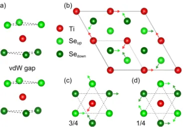
In pristine 1T -stacked TiSe2 [Fig. 1(a)], there are two
possible PLD-related sites for the eight Ti structural atoms of the 2× 2 × 2 CDW unit cell. Indeed, six of them experience a displacement inducing a Ti-Se bond shortening [referred to as the34conformation, Fig.1(c)], whereas the two remaining ones are concerned by a rotation of the six neighboring Se atoms that only slightly changes the Ti-Se interatomic distances [referred to as the14 conformation, Fig.1(d)].
In Ti self-doped 1T -TiSe2 crystals, Ti defects are
interca-lated in the van der Waals (vdW) gap directly in line with the structural Ti atoms [Fig.1(a)] [7]. Therefore, the CDW phase transition intrinsically implies two nonequivalent sites in the unit cell for each Ti defect, with also three times more34 sites
FIG. 1. (a) Structural model of 1T -TiSe2. (b) Top view (along the caxis) of the PLD accompanying the 1T -TiSe2CDW phase transition
(the atomic displacements are represented by arrows). The dotted and solid black lines represent the unit cells of the normal phase and of the CDW superstructure, respectively. (c), (d) Top views of the 1T -TiSe2
atomic structure showing the PLD displacements with 34 of TiSe6
octahedra distorted by Ti-Se bond shortening (c), and 1
4 concerned
by a rotation of the Se atoms around a nonmoving Ti atom (d).
than14ones [18]. Since the six TiSe6octahedra concerned with
Ti-Se bond shortening are energetically favorable with respect to the undistorted structure, and the two rotating octahedra are not [19], it becomes highly desirable to investigate the impact of nonequivalent Ti dopants sites on the local electronic properties of the CDW.
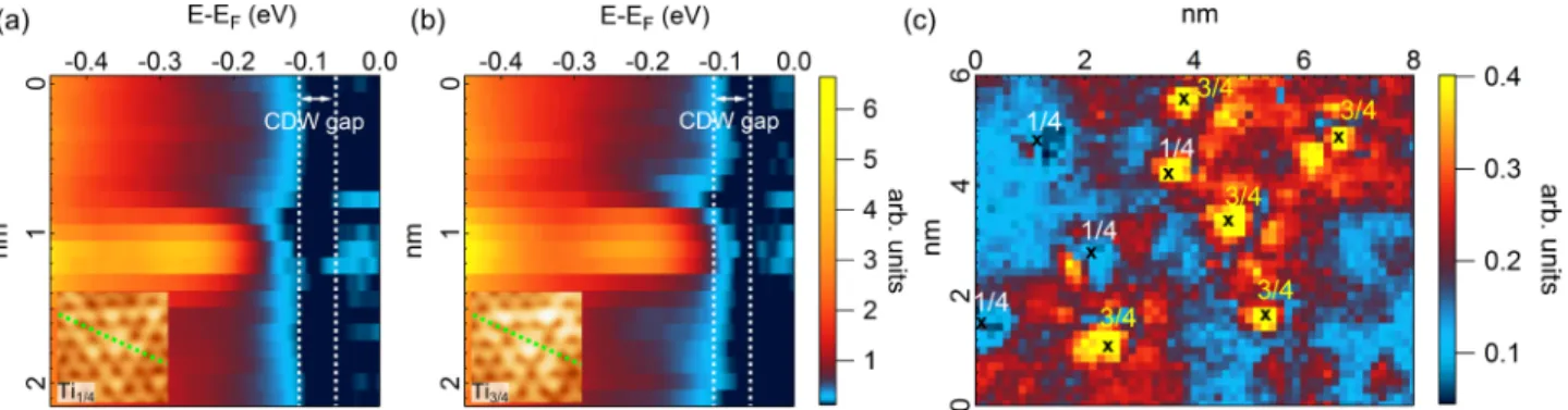
Figures2(a)and2(b)present 8× 6 nm2filled- and empty-state STM images of the 1T -TiSe2 surface respectively
recorded at−50 and +100 mV. The high-resolution filled-state STM image close to EF [Fig.2(a)] clearly shows the
atom-ically resolved CDW superstructure and the presence of one atomically sharp phase slip [gray line, Fig.2(a)], separating two commensurate CDW domains, as expected from the used Ti-doping density and associated CDW domain sizes [6].
The nonequivalent intercalated-Ti atoms are best resolved and differentiated at positive Vbias[18]. Empty-state STM images
[Fig.2(b)] reveal their characteristic nonidentical patterns con-sisting of two concentric bright triangles centered on the defect and CDW maxima locations with respect to the underlying Se atomic layer that depend on their1
4 or 3
4 conformations [18].
Figure2(c)shows tunneling spectra at specified sites of the 1T -TiSe2 surface. Each tunneling curve has been measured
at different but equivalent positions of the surface and have shown to be highly reproducible [20]. In defect-free surface regions, the LDOS corresponds to the one of the CDW state in an overall electron-doped 1T -TiSe2 crystal [red curve in
Fig.2(c)]. Indeed, the DOS is nonzero at EF and shows a
slight drop of the electron density that corresponds to the Ti 3d conduction band in the CDW state. The CDW gap [indicated by the arrow between the dashed lines, Fig.2(c)], separating the occupied Se 4p orbitals and the Ti 3d electron pocket, opens below EFbetween∼ − 110 and ∼ − 60 mV [21].
The nonequivalent nature of the intercalated-Ti atoms is also clearly manifested in the filled-state part of the STS curves made on top of the14and34 conformations [light and dark blue curves in Fig.2(c)]. Indeed, ∼200–300 mV below EF, the
induced electron-donor impurity states of mixed Ti 3d-Se 4p orbital character are energetically nondegenerate with the one associated with the14-conformed Ti defects lower in energy by ∼50 mV [arrow between the solid black lines in Fig.2(c)] in such a way that the34impurity state starts to overlap the CDW gap below EF.
Figures 3(a) and 3(b) show position-dependent intensity plots of the LDOS below EF. The associated dI /dV curves
have been measured as a function of position through the 14 and34 intercalated-Ti defects, respectively, with an interval of 1.4 ˚A [dotted green lines in the insets of Figs.3(a)and3(b)]. They clearly demonstrate the spatial variation of the LDOS and allow one to compare the extension of the CDW perturbations introduced by the nonequivalent Ti dopants.
At the intercalated-Ti sites [profiles with the highest intensity, Figs.3(a)and3(b)], the LDOS associated with the
FIG. 2. (a) 8× 6 nm2constant current STM image of the 860◦C-grown 1T -TiSe
2 crystal showing the CDW charge modulation within
two phase-shifted CDW domains separated by one phase slip. Two meshes corresponding to the two phase-shifted CDW modulations are superimposed and the phase-slip location is indicated by the full gray line. Vbias= −50 mV, I = 0.2 nA. (b) Constant current STM image
at 100 mV bias voltage and 0.2 nA current set point of the same region as (a), highlighting the characteristic fingerprints of the 14 and 34 intercalated-Ti conformations in the presence of CDW (black squares on the left- and right-hand sides, respectively). (c) dI /dV curves on top of the two intercalated-Ti conformations (light and dark blue curves, each of them averaged over five spectra) and on defect-free region (red curve, averaged over 18 spectra).
FIG. 3. (a), (b) Position-dependent intensity plots of the LDOS between−450 mV and EF. Ten dI /dV curves have been measured as a
function of position with an interval of 1.4 ˚A, through the1 4 and
3
4 intercalated-Ti defects as indicated by the dotted green lines in the insets.
Identical color scales have been used in (a) and (b). The white dashed lines in (a) and (b) mark the CDW gap region between∼ − 110 and ∼ − 60 mV. (c) Real-space dI/dV map obtained at Vbias= −110 mV on the same region as Figs.2(a)and2(b)showing the real-space CDW
gap perturbation due to intercalated-Ti atoms. The positions of1 4- and
3
4-conformed Ti defects are also indicated.
1
4 and
3
4 conformations shows the electron-donor impurity
states that both develop ∼200–300 mV below EF on a
relatively short length scale. Although at these energies they introduce electronic perturbations of the topmost Se layer electronic density of limited spatial extension that relates to the localized nondispersing nature of intercalated-Ti 3d orbitals, the impact of their PLD-related conformations on the CDW gap is nonequivalent [CDW gap region between∼ − 110 and ∼ − 60 mV as indicated by the white dashed lines in Figs.3(a) and3(b)]. Indeed, the 34 impurity state overlaps the CDW gap [Fig.3(b)] much more than the 14-conformed one [Fig.3(a)]. The dI /dV map obtained at Vbias= −110 mV [Fig.3(c)], i.e.,
at the occupied edge of the CDW gap, shows a higher DOS at and around the 34 intercalated-Ti atoms therefore indicating a more extended real-space electronic perturbation of the CDW gap as well as of defect states in their immediate vicinity [see the 1
4-conformed Ti defect at coordinates (3.6,4.2) nm in
Fig.3(c)]. This demonstrates that the34-conformed Ti defects have an overall detrimental effect on the CDW state and points towards their higher capability to destroy the CDW order.
Interestingly, statistics made on the relative density of the
1
4 and
3
4 Ti defect conformations finally provide an additional
key point for understanding the occurrence of CDW phase slips, i.e., the loss of the long-range phase coherence of the CDW state in Ti self-doped 1T -TiSe2 crystals. It is known
that increasing Ti doping dramatically influences the CDW by breaking it into phase-shifted domains [6]. Whereas for low Ti doping, the CDW exhibits a long-range order and a perfect distribution of the 1
4 (25%) and 3
4 (75%) Ti-defect
sites [18], for the studied highly doped crystal, a careful analysis of 65 intercalated-Ti atoms in the presence of CDW modulation shows that more than 35% of them have a 14 conformation [instead of 25%, as clearly depicted in Figs.2(b) and3(c), where already four out of nine Ti defects are in 14 conformation].
This finding indicates that intercalated-Ti defects do not act as a fixed random landscape that can be described by a unique perturbation potential, as it is the case in the well-known impurity pinning theory initially proposed by McMillan [22], and further extended in the Fukayama-Lee-Rice models of weak and strong impurity pinning [23–25]. Rather, even if
the Ti defects are fixed, their spatial distribution with respect to the PLD can be accommodated by the CDW through the phase-slip creation that allows one to introduce an imbalance in their statistical distribution in favor of the14Ti conformation. The loss of long-range phase coherence therefore appears as a local resilient behavior of the CDW to Ti self-doping and constitutes a different mechanism highlighting the key role of the PLD-induced defect degree of freedom for the understanding of the CDW phase patterning in intercalated TiSe2compounds [6,26–28].
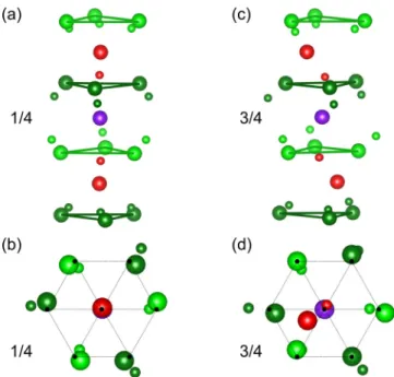
Finally, we would like to address the crucial role of the electron-lattice interaction that lies behind the induced imbalance in intercalated-Ti conformations and that is closely related to the nonequivalent CDW gap perturbation. DFT calculations performed for the two nonequivalent Ti defects in the vdW gap of the PLD-distorted 1T -TiSe2lattice confirm
that the total energy is lower for the14 conformation (70 meV per intercalated-Ti atom). Looking at the associated structures after relaxation (Fig.4), we first see that for the14conformation [Fig. 4(a)], the lattice distortion is very close to the one calculated for a non-CDW cell [6]. The atomic displacements are fully symmetric with respect to the14intercalated-Ti defect [Fig.4(b)], therefore leaving unchanged the threefold symme-try of the CDW, as confirmed by our STM measurements [inset of Fig.3(a)].
On the contrary, as experimentally observed [inset of Fig.3(b)], the lattice distortion induced by 34-conformed Ti defects clearly breaks the CDW threefold symmetry [Figs.4(c) and4(d)], with a calculated magnitude of displacements 11% larger than the one calculated in the 14 cell. Indeed, the
3
4-conformed Ti defects induce large lateral displacements of
the two neighboring Ti structural atoms [Figs.4(c)and4(d)], in such a way that the energetically favorable TiSe6octahedra
concerned with Ti-Se bond shortening (2.49 ˚A, as obtained by DFT) in pristine 1T -TiSe2 undergo a Ti-Se bond elongation
of 2% (2.54 ˚A) under Ti intercalation.
Based on our STM/STS measurements and DFT calcula-tions, we can thus draw the following conclusions. The atomic displacements as well as the electronic perturbation of the CDW gap induced by the34 intercalated-Ti conformation are larger than those induced by the14one. The fact that the CDW
FIG. 4. DFT-calculated relaxed structures of the 2× 2 × 2 1T -TiSe2 lattice with (small spheres) and without (large spheres)
intercalated-Ti atoms (violet spheres). Two TiSe6octahedra separated
by one vdW gap are considered. (a), (b) and (c), (d): Side and top views (top TiSe6octahedron along the c axis) for the 14, respectively
3
4, Ti-defect conformation. The amplitude of displacements induced
by Ti intercalation have been enhanced by a factor of 10. The black dots in (b) and (d) indicate the atomic positions in the non-CDW cell, i.e., without PLD.
avoids perturbing the PLD-related 34 conformation with a Ti impurity by favoring the 14 defect conformation is evidence for the predominant role of the Ti-Se bond shortening for the stabilization of the modulated structure of 1T -TiSe2, as
proposed in the pseudo Jahn-Teller scenario [19]. Therefore, with the increase of intercalated-Ti density, it becomes energetically favorable to introduce CDW domain boundaries since the cost in elastic energy starts to be compensated by the electronic energy gain brought by the induced Ti-conformation imbalance.
To summarize, our site-specified STM/STS study of Ti-doped 1T -TiSe2 crystals allows a deep investigation of the
impact of nonequivalent dopant sites on the local electronic properties of the CDW. The ability of the CDW state to locally determine the PLD-related conformation of intercalated atoms not only constitutes a different CDW-impurity interaction mechanism, but also highlights the underlying role of the dopant landscape for CDW phase patterning, resulting in spatially modulated electronic states that are expected to be a key ingredient for the emergence of mixed CDW-superconducting phases in Cux-TiSe2 [26–28], and TMDCs
in general [9–11].
This project was supported by the Fonds National Suisse pour la Recherche Scientifique through Div. II. We would like to thank C. Monney, H. Beck, A. M. Novello, and C. Renner for motivating discussions. Skillful technical assistance was provided by F. Bourqui, B. Hediger, and O. Raetzo.
B.H. and T.J. equally contributed to this work.
[1] F. Di Salvo, D. Moncton, and J. Waszczak,Phys. Rev. B 14,
4321(1976).
[2] E. Morosan, H. W. Zandbergen, B. S. Dennis, J. W. G. Bos, Y. Onose, T. Klimczuk, A. P. Ramirez, N. P. Ong, and R. J. Cava,
Nat. Phys. 2,544(2006).
[3] A. F. Kusmartseva, B. Sipos, H. Berger, L. Forr´o, and E. Tutiˇs,
Phys. Rev. Lett. 103,236401(2009).
[4] Y. I. Joe, X. M. Chen, P. Ghaemi, K. D. Finkelstein, G. A. de la Pe˜na, Y. Gan, J. C. T. Lee, S. Yuan, J. Geck, G. J. MacDougall, T. C. Chiang, S. L. Cooper, E. Fradkin, and P. Abbamonte,Nat. Phys. 10,421(2014).
[5] L. J. Li, E. C. T. O’Farrell, K. P. Loh, G. Eda, B. ¨Ozyilmaz, and A. H. Castro Neto,Nature (London) 529,185(2015).
[6] B. Hildebrand, T. Jaouen, C. Didiot, E. Razzoli, G. Monney, M.-L. Mottas, A. Ubaldini, H. Berger, C. Barreteau, H. Beck, D. R. Bowler, and P. Aebi,Phys. Rev. B 93,125140(2016). [7] B. Hildebrand, C. Didiot, A. M. Novello, G. Monney, A.
Scarfato, A. Ubaldini, H. Berger, D. R. Bowler, C. Renner, and P. Aebi,Phys. Rev. Lett. 112,197001(2014).
[8] D. Bhoi, S. Khim, W. Nam, B. S. Lee, C. Kim, B.-G. Jeon, B. H. Min, S. Park, and K. H. Kim,Sci. Rep. 6,24068(2016). [9] Y. Liu, D. F. Shao, L. J. Li, W. J. Lu, X. D. Zhu, P. Tong, R. C.
Xiao, L. S. Ling, C. Y. Xi, L. Pi, H. F. Tian, H. X. Yang, J. Q. Li, W. H. Song, X. B. Zhu, and Y. P. Sun,Phys. Rev. B 94,045131
(2016).
[10] R. Ang, Z. C. Wang, C. L. Chen, J. Tang, N. Liu, Y. Liu, W. J. Lu, Y. P. Sun, T. Mori, and Y. Ikuhara,Nat. Commun. 6,6091
(2015).
[11] R. Ang, Y. Tanaka, E. Ieki, K. Nakayama, T. Sato, L. J. Li, W. J. Lu, Y. P. Sun, and T. Takahashi,Phys. Rev. Lett. 109,
176403(2012).
[12] E. Morosan, K. E. Wagner, L. L. Zhao, Y. Hor, A. J. Williams, J. Tao, Y. Zhu, and R. J. Cava, Phys. Rev. B 81, 094524
(2010).
[13] L. Fang, Y. Wang, P. Y. Zou, L. Tang, Z. Xu, H. Chen, C. Dong, L. Shan, and H. H. Wen, Phys. Rev. B 72, 014534
(2005).
[14] G. Kresse and J. Hafner,Phys. Rev. B 47,558(1993). [15] G. Kresse and J. Furthm¨uller, Phys. Rev. B 54, 11169
(1996).
[16] G. Kresse and D. Joubert,Phys. Rev. B 59,1758(1999). [17] J. P. Perdew, K. Burke, and M. Ernzerhof,Phys. Rev. Lett. 77,
3865(1996).
[18] A. M. Novello, B. Hildebrand, A. Scarfato, C. Didiot, G. Monney, A. Ubaldini, H. Berger, D. R. Bowler, P. Aebi, and C. Renner,Phys. Rev. B 92,081101(R)(2015).
[19] M. H. Whangbo and E. Canadell,J. Am. Chem. Soc. 114,9587
(1992).
[20] The STS curves of Fig.2(c)have been renormalized on the basis of the STM topography image made in parallel to the STS map
for correcting the exponential decay of the tunneling current associated with the different tip-surface distances on top of a Ti defect.
[21] C. Monney, H. Cercellier, F. Clerc, C. Battaglia, E. F. Schwier, C. Didiot, M. G. Garnier, H. Beck, P. Aebi, H. Berger, L. Forr´o, and L. Patthey,Phys. Rev. B 79,045116(2009).
[22] W. L. McMillan,Phys. Rev. B 12,1187(1975). [23] P. A. Lee and T. M. Rice,Phys. Rev. B 19,3970(1979). [24] H. Fukuyama and P. A. Lee,Phys. Rev. B 17,535(1978).
[25] P. A. Lee and H. Fukuyama,Phys. Rev. B 17,542(1978). [26] S. Yan, L. Davide, E. Morosan, E. Fradkin, P. Abbamonte, and
V. Madhavan,arXiv:1609.08249.
[27] A. M. Novello, M. Spera, A. Scarfato, A. Ubaldini, E. Giannini, D. R. Bowler, and C. Renner, Phys. Rev. Lett. 118, 017002
(2017).
[28] A. Kogar, G. A. de la Pena, S. Lee, Y. Fang, S. X.-L. Sun, D. B. Lioi, G. Karapetrov, K. Finkelstein, J. P. C. Ruff, P. Abbamonte, and S. Rosenkranz,Phys. Rev. Lett. 118,027002(2017).