HAL Id: hal-00142999
https://hal.archives-ouvertes.fr/hal-00142999
Submitted on 30 Jul 2007
HAL is a multi-disciplinary open access
archive for the deposit and dissemination of
sci-entific research documents, whether they are
pub-lished or not. The documents may come from
teaching and research institutions in France or
abroad, or from public or private research centers.
L’archive ouverte pluridisciplinaire HAL, est
destinée au dépôt et à la diffusion de documents
scientifiques de niveau recherche, publiés ou non,
émanant des établissements d’enseignement et de
recherche français ou étrangers, des laboratoires
publics ou privés.
A DfT Architecture for Asynchronous Networks-on-Chip
Xuan Tu Tran, Jean Durupt, François Bertrand, Vincent Beroulle, Chantal
Robach
To cite this version:
Xuan Tu Tran, Jean Durupt, François Bertrand, Vincent Beroulle, Chantal Robach. A DfT
Archi-tecture for Asynchronous Networks-on-Chip. The 11th IEEE European Test Symposium, May 2006,
Southampton, United Kingdom. pp.219-224, �10.1109/ETS.2006.3�. �hal-00142999�
A DFT Architecture for Asynchronous Networks-on-Chip
Xuan-Tu TRAN, Jean DURUPT,
and Franc¸ois BERTRAND
LETI – CEA
17, rue des Marstyrs, 38054 Grenoble, France
[email protected]
Vincent BEROULLE,
and Chantal ROBACH
LCIS – INPG
50, rue Barthlmy de Laffemas, Valence, France
[email protected]
Abstract
The Networks-on-Chip (NoCs) paradigm is emerging as a solution for the communication of SoCs. Many NoC archi-tecture propositions are presented but few works on testing these network architectures.
To test the SoCs, the main challenge is to reach into the embedded cores (i.e, the IPs). In this case, the DFT tech-niques that integrate test architectures into the SoCs to ease the test of these SoCs are really favoured. In this paper, we present a new methodology for testing NoC architectures. A modular, generic, scalable and configurable DFT tecture is developed in order to ease the test of NoC archi-tectures. The target of this test architecture is asynchronous NoC architectures that are implemented in GALS systems. The proposed architecture is therefore named ANoC-TEST and is implemented in QDI asynchronous circuits. In ad-dition, this architecture can be used to test the computing resources of the networked SoCs. Some initial results and conclusions are also given.
1. Introduction
A global shared-bus cannot meet the needs of communi-cation on a System-on-Chip (SoC) because long-wire loads, resistances and shared bandwidth result in slow signal prop-agation. An alternative solution, the bus hierarchical archi-tecture, presented by [1], becomes a provisional solution but still faces many constraints in on-chip interconnections.
Network-on-Chip (NoC) paradigm is emerging as a promised solution for the communication of SoCs with nu-merous advantages in comparison with bus-based SoC ar-chitectures: good efficiency, high scalability and versatility, as well as high bandwidth communication [2–4].
With this innovation, NoC-based SoCs integrate more and more Intellectual Property (IP) blocks into a single chip. This gives many challenges to designers and also makes the
test of SoCs more difficult. In addition, the IPs are hierar-chically embedded into the IPs, and the systems are divided into many parts with different clocks and design technolo-gies.
To test a common core-based SoC, the challenge is to access to the embedded cores. A general architecture to test the embedded cores in core-based SoCs has been first proposed in [5]. In this architecture, the embedded cores are covered by wrappers that with test access mechanisms (TAMs) improve the controllability and the observability of the embedded cores. In order to make this design-for-test (DFT) methodology for the embedded cores become reusable, a standard for embedded core test has been devel-oped, IEEE 1500 Standard for Embedded Core Test [6]. In the age of NoC-based SoCs, to test a SoC we must deal with two main issues: the test of the IP cores that are embedded in the SoC and the test of the communication networks (i.e., the NoC architectures) [7].
Many propositions of NoC architectures for SoCs de-sign have been presented, such as SoCBUS [8], NOS-TRUM [9], SPIN [10], HERMES [11], xPIPES [12], ÆTHEREAL [13], QNOC [14], PROTEO [15], OC-TAGON [16], but works on testing the NoC architectures are few. Some works presented in [17,18] reuse the on-chip communication networks as TAMs to reach into the embed-ded cores. Test vectors are transported from the test vector generator to the embedded cores under test and the test re-sults are transported from the embedded cores under test to the analyzer via the on-chip networks. The advantages of this technique are low cost overhead and high bandwidth TAM for testing of embedded cores. Some other litera-tures discuss on testing of NoC architeclitera-tures (i.e., testing the communication networks) [2, 7], but no solution is pro-posed. A.M. Amory et al. [19] presents a methodology to test the synchronous network routers but it remains the test of internode wires and network interfaces.
In addition, the above NoC propositions solve most of the SoCs problems but do not cover the problem of multi-clocks used in SoC designs. In [20], the CEA-LETI has
proposed an asynchronous NoC (ANoC) architecture that is used for Global Asynchronous – Local Synchronous (GALS) platforms. This ANoC architecture, nodes and their interconnections, is implemented in asynchronous cir-cuits. It allows using multi-clocks for NoC-based SoCs design, a different clock for each distinct IP block. With the same approach, some other works have been proposed such as CHAIN [21], NEXUS [22], etc. All of these asynchronous NoC architectures adapt well for GALS plat-forms. They are the best solutions for the interconnection of SoCs with different clock domains and design technologies but they give also a huge difficulty for the manufacturing test because of many feedback loops.
The goal of our work is to develop an innovative method-ology to test the asynchronous NoC architectures. In this paper we introduce a modular, generic, scalable and config-urable architecture to ease the test of asynchronous NoC ar-chitectures. This DFT architecture targets the asynchronous NoC architecture presented in [20]. It is therefore named ANoC-TEST architecture.
The paper is organized as follows. Section 2 presents briefly the context and objectives of this work; Section 3 is a recall of the ANoC architecture, for which we develop a test method; Section 4 presents an innovative DFT architec-ture for testing the asynchronous NoC architecarchitec-tures, applied for the ANoC architecture; Section 5 presents the design of the proposed architecture; and finally design results and conclusions are given in Section 6.
2. How to Test NoC-based Systems-on-Chip
In NoC-based SoCs, we can imagine that the NoC com-munication architectures look like embedded cores with many identical sub-cores, nodes and network interfaces (NIs). Testing a NoC-based SoC for manufacturing defects can be categorized into two issues: the test of the NoC com-munication architectures; and the test of the computing re-sources (i.e., the IPs). Some works in [17, 18] reused the NoC communication architectures as TAMs to test the IP cores. However, making sure that the NoC communication architectures have no defect should be done first. If the NoC communication architectures contain defects, the following actions can be proposed: elimination of the die, use of a degraded mode, or replacement of the defective logics by redundant logics.
To test the NoC communication architectures, a simple method that the test stimuli are transported on the networks as communication packets may be used. This method does not need additional logics but it is insufficient to cover all possibilities of defects, for example, arbitration faults in case of concurrent data paths. In addition, when a fault is detected, we do not know where it is.
3. ANoC: an Asynchronous NoC Architecture
for GALS Systems
The CEA-LETI has proposed a low latency Asyn-chronous Network-on-Chip (ANoC) architecture in [20]. This ANoC communication architecture is composed of network nodes, links between nodes, and asyn-chronous/synchronous NIs between asynchronous nodes and synchronous resources. The nodes are the basic el-ements of the network and they usually have five bi-directional ports that connect to four neighboring nodes and the nearest synchronous computing resource via an asyn-chronous/synchronous NI. The role of nodes is to compute where to transmit an incoming data, then to arbitrate be-tween potential concurrent data, and finally to transmit the selected data to the selected output. All of these nodes are implemented in Quasi-Delay Insensitive (QDI) asyn-chronous logics in order to adapt GALS platforms and allow to use multi-clocks in different IPs.
4. ANoC–TEST: a Proposition for Testing NoC
Architectures
4.1. Architecture description
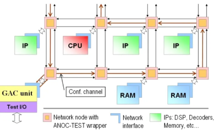
Figure 1. ANoC-TEST: a general architecture.
Because NoC architectures may be imagined as em-bedded cores, some principles of the IEEE 1500 Standard for Embedded Core Test therefore may be used. A gen-eral architecture of ANoC-TEST is illustrated in Figure 1. The ANoC-TEST architecture includes test wrappers that cover the network nodes, a configuration channel, and a generator-analyzer-controller (GAC) unit used to generate test vectors, analyze test results, and control the configura-tion channel. Specially, to adapt well to the asynchronous NoC architectures, the test wrapper is implemented by us-ing asynchronous cells instead of usus-ing classical shift reg-isters with a clock signal. The communication between
these cells is realized by handshake signals. Additionally, the network wires are reused to transport test stimuli and test results as high bandwidth TAMs. It is why the IEEE-compliant test wrapper is not used.
With this test architecture, the test vectors generated by the GAC unit are transported to the nodes-under-test via the network wires and are loaded to the nodes by the ANoC-TEST wrappers. In the other side, the test results are with-drawn by the ANoC-TEST wrappers and transported to the GAC unit via the network wires for analyzing. All the oper-ations of ANoC-TEST wrappers are configured by the con-figuration channel and the actions of the concon-figuration chan-nel is operated by a finite state machine in the GAC unit. The GAC unit may be implemented on-chip as an IP, or off-chip as a computer program which communicates with the ANoC via I/O ports, or an Ethernet port. In the following subsections we focus on the design of ANoC-TEST wrap-pers, the most important parts of the ANoC-TEST architec-ture.
4.2. ANoC-TEST wrapper
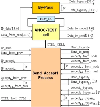
Figure 2. Connections between 2 wrappers.
In corresponding to the number of ports of the ANoC node, the ANoC-TEST wrapper is composed of five input stage cells, five output stage cells, and a local test control module (TCM). Two asynchronous 5/5 test wrappers and their communication channels are presented in Figure 2. The TCMs are serially interconnected to establish a config-uration channel in order to control the input/output stages of the test wrappers. The role of the ANoC-TEST wrapper is to transport test vectors to the node-under-test in correct situations and get the test results from the node-under-test through many operations: updating test vectors (update new test vectors to the input cell); shifting test vectors (shift the test vectors to the targeted input cell); loading test vectors (load the test vectors to the node-under-test); withdrawing test results (withdraw the test results from the node-under-test); shifting test results (shift the test results to the tar-geted output cell); transmitting test results (transmit the test
results to the TAMs); etc. To improve the quality of ser-vices (QoS), the asynchronous NoC presented in [20] uses
k virtual channels with k levels of priority. All these
lev-els of priority are arbitrated so that only one virtual channel is established at a time. Obviously, the test wrapper has to make no change to the values of data and their levels of pri-ority. The details of ANoC-TEST wrapper are presented as follows:
Input stages: In test mode, the input stage cell
trans-mits an incoming flit from the network or from the previous cell to the node-under-test or to the next cell, correspond-ing to the control signals that derive from TCM module. The main goal of the input stages is to transmit the test vec-tor to the node-under-test on correct input ports. If a shift or a load operation is requested, the incoming test vector will be stored in an immediate buffer, named “Buff R0”. In asynchronous design, this buffer is easily realized by com-munication channels in the input stage cells. Then, the test vector may be shifted to the next cell or loaded to the node at the next communication cycle. All “Send” and “Accept” signals are combined and generated inside this input stage.
The architecture of the input stage for anN -inputs/
out-puts node and k priority levels is presented in Figure 3,
where the “Buff R0” is just a symbolic view of the imme-diate buffer.
Figure 3. Input stage of the wrapper.
To reduce test time, a bypass function is usually favoured. If a bypass operation is required by the TCM module, the input stage will establish a bypass channel in
order to transmit directly the incoming test data from the network to the selected bypass output (depending on the di-rection we want to realize a bypass).
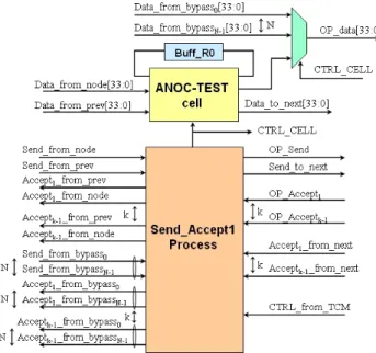
Output stages: In test mode, the output stage cell
trans-mits an incoming flit from the node-under-test or from the previous cell to the network or to the next cell, correspond-ing to the control signals that derive from TCM module. The main goal of the output stages is to withdraw the test re-sults from the node-under-test and transport them to the test result analyzer. If a shift or an export operation is requested, the incoming test result will be updated in an immediate buffer, “Buff R0”. As in the input stages, this buffer is real-ized by communication channels. Then, the test result may be shifted to the next cell or exported to the output port at the next communication cycle. All “Send” and “Accept” signals are combined and generated inside this output stage. The architecture of the output stage for anN -inputs/
out-puts node and k priority levels is presented in Figure 4,
where the “Buff R0” is just a symbolic view of the imme-diate buffer.
Figure 4. Output stage of the wrapper.
If a bypass operation is required, the output stage will se-lect a bypass channel that is established by the correspond-ing input stage and the test data from this bypass channel will be directly transported to the output port.
Test Control Module: The local test control module
(TCM) is composed by a multiplexer and two registers, see Figure 5, a register is used for building a configuration chan-nel and the other one is used for updating test instructions. The instruction bypass is simply realized by a bypass mul-tiplexer in the TCM module. This mulmul-tiplexer is controlled by a flag in the update instruction register, the flag is named
“bypass flag”. If this flag is set, the control data input of the TCM module will be connected directly to the control data output. This technique allows to reduce efficiently the test time. If a node is put in test mode and the others are put in bypass mode, the node-under-test is directly connected to the GAC unit in both of data and configuration channels.
The update of test instructions is realized by an instruc-tion update signal from the GAC unit. The “Send” and “Accept” signals of the control data channel are combined and generated inside this module by “send–accept” process. The output control signals,CT RL < i >, are used to
de-cide the operations of the input and output stage cells.
Figure 5. A local Test Control Module (TCM).
4.3. ANoC-TEST Configuration
With the architecture described above, the ANoC-TEST wrapper is configured to get test vectors from the network wires and load them to the node-under-test, then to with-draw the test results from the node-under-test and transmit them to the network wires. It may be easily configured in the following modes:
Normal Mode: In normal mode (i.e., transparent mode),
the ANoC-TEST wrapper is transparent. The network nodes operate as if they are not covered by the test wrap-per. The inputs of the ANoC-TEST wrapper’s input stages are directly connected to the inputs of the ANoC node and the outputs of the ANoC node are directly connected to the outputs of ANoC-TEST wrapper’s output stages.
Test Mode: In test mode, there are two main sub-modes:
testing the node-under-test and testing the surrounding con-nections. When a test process is enable, the GAC unit es-tablishes the configuration channel in order to configure the nodes in bypass mode or in test mode. Then, the GAC unit activates the instruction-update operation to put these nodes in the selected modes.
When nodes-under-test are defined, the configuration channel and the test data channel are directly connected to
the wrappers of these nodes. The GAC unit now controls the test wrappers to transmit the test vectors to the inputs of the nodes and to withdraw the test results from the outputs of these nodes by a set of operations as described above: update, shift, load, withdraw, export, etc. The testing pro-cess will be stopped when the reset signal is set. To realize an other test process, the configuration channel must be re-established. Depending on the test configuration, a node or more is set under test mode.
Bypass Mode: In order to reduce the test time, the
by-pass mode is developed. This mode allows us to isolate each node from the others and to do the test of this node only. The advantages of this mode is not only to reduce test time, but also to allow us to know exactly where the faulty node is. In addition, the bypass mode also makes the testing processes become easier.
5. Design and Verification
5.1. Flit-level handshake protocol
The handshake protocol is used to interconnect between the wrappers and between the wrappers and the nodes to ex-change a data flit. The flit handshake protocol in our archi-tecture is defined as the “Send/Accept” protocol, in which the communication between two wrappers or between a wrapper and a node is performed via the “Send” and “Ac-cept” signals, see Figure 6. To establishk virtual
chan-nels in the network, this flit handshake protocol is imple-mented byk “Send” and k “Accept” signals: send < i >
andaccept < i >, where i gets values from 0 to k − 1.
And the sender is allowed to send a new flit on virtual chan-nel i with send < i >= 1, if and only if, the receiver
indicatedaccept < i >= 1 at the previous cycle. With
this “Send/Accept” protocol, flit transactions are realized in many virtual channel with an assurance of free physi-cal channel. In practice, we have implemented the ANoC-TEST architecture withk equals 2.
Figure 6. Flit-level “Send/Accept” signaling.
5.2. QDI asynchronous design
To design the ANoC-TEST wrapper, the Quasi-Delay Insensitive (QDI) asynchronous design style [23] is used.
We have used a 4-phase RTZ protocol signaling for asyn-chronous channels. To have low power consumption, the 1-of-4 code signaling is used [24].
5.3. Verification platform
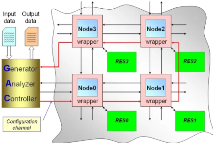
The ANoC-TEST wrapper has been modeled in Sys-temC/C++ and validated by using a test bench model that is illustrated in Figure 7. The role of the GAC unit is to gen-erate test vectors, to receive the test results, and to control the operations of all other blocks in the test bench model. It is also done in SystemC/C++. In fact, the generation of test vectors and the establishment of configuration channel are simply realized by reading test data and test configura-tion files. The test results are received and stored in a test result file that will be compared with the source test data file. In addition, the values of the configuration channels are re-read and stored in a test result file in order to allow a verification of configuration operations.
Figure 7. A test-bench with 4 test wrappers.
6. Results and Conclusion
The design of the proposed architecture is generic and can be adapted to the number of virtual channels required by the ANoC. The modularity of the ANoC-TEST is expressed through the independence of the test wrappers and theirs im-plementation in asynchronous logic. In addition, this archi-tecture may be easily configured to test many nodes at the same time, in parallel. In this case, thanks to the identity of the network nodes, the test vectors are simultaneously ap-plied in parallel and the test responses can be compared to each other. The test of NIs and the test of IPs can be ef-ficiently realized by configuring the test wrappers to have bypasses to the IP-under-test.
In term of reuse, the network wires are reused as high bandwidth TAMs and the test vectors can be reused for all
nodes. The reuse of network wires allows to reduce the sur-face and to avoid the wiring congestion in layout process. In test mode, the maximum TAM throughput of each test path is about 1 Gbytes/s for an average communication de-lay corresponding to an equivalent frequency of 250 MHz and 32-bits width.
The proposed architecture is scalable and can be ex-panded to accommodate to the size of the ANoC by adding the test wrappers in corresponding to the number of the net-work nodes, while the test time and test data volume in-crease little thanks to the possibility of test in parallel and high throughput TAMs.
The ANoC-TEST wrapper architecture is modeled and validated in a SystemC/C++ environment that corresponds to the behaviours of asynchronous circuits. The surface cost of this wrapper is evaluated at about 8000 gates. It is incon-siderable compared to the surface cost of our test target, an asynchronous NoC with 20 nodes, 23 IPs, and a total sur-face of 4.5 Mgates without memories.
References
[1] ARM Inc. AMBA On-chip Bus Architecture.
http://arm.com/products/solutions/AMBAHomePage.html
[2] A. Jantsch and H. Tenhunen. Networks on Chip. Kluwer Aca-demic Publisher, Feb. 2003.
[3] L. Benini and G. De Micheli. Networks on Chip: a New SoC Paradigm. IEEE Computer, Vol. 1, pp. 70–78, Jan. 2002. [4] W. J. Dally and B. Towless. Route Packets, not Wires:
On-Chip Interconnection Networks. In Proc. of the Design
Au-tomation Conf. (DAC), pp. 684–689, NV, USA, June 2001.
[5] Y. Zorian. Testing Embedded-Core based System Chips. In
Proc. of the Int’l Test Conference (ITC), pp. 130–140,
Wash-ington, DC, USA, Oct. 1998.
[6] IEEE Std. 1500. IEEE 1500 Standard for Embedded Core Test. http://grouper.ieee.org/groups/1500/.
[7] B. Vermeulent, J. Dielissen, K. Goossens, and C. Ciordas. Bringing Communication Networks on a Chip: Test and Verification Implications. IEEE Communication Magazine, pp. 74–81, Sep. 2003.
[8] D. Wiklund and D. Liu. SoCBUS: Switched Network on Chip for Hard Real Time Embedded Systems. In Proc. of the Int’l
Parallel and Distributed Processing Symposium (IPDPS),
Nice, France, April 2003.
[9] S. Kumar et al. A Network on Chip Architecture and Design Methodology. In Proc. of the IEEE Computer Society Annual
Symposium on VLSI (ISVLSI), pp. 105–112, USA, April 2002.
[10] P. Guerrier and A. Greiner. A Generic Architecture for On-Chip Packet-Switched Interconnection. In Proc. of the
De-sign, Automation and Test in Europe (DATE), pp. 250–256,
Paris, France, March 2000.
[11] F. Moraes et al. HERMES: an Infrastructure for Low Area Overhead Packet-Switching Networks on Chip. Integration,
the VLSI Journal, 38(1):69–93, Oct. 2004.
[12] M. Dall’Osso et al. xPIPES: a Latency Insensitive Param-eterized Network-on-Chip Architecture for Multi-Processors SoCs. In Proc. of the 21st Int’l Conf. on Computer Design
(ICCD), pp. 536–539, San Jose, California, USA, Oct. 2003.
[13] E. Rijpkema et al. Trade Offs in the Design of a Router with both Guaranteed and Best-Effort Services for Networks on Chip. In Proc. of the Design, Automation and Test in Europe
(DATE), pp. 10350–10355, Germany, March 2003.
[14] E. Bolotin, I. Cidon, R. Ginosar, and A. Kolodny. QNOC: QoS Architecture and Design Process for Network on Chip.
Journal of Systems Architecture: The Euromicro Journal,
50(2–3):105–128, Feb. 2004.
[15] I. Saastamoinen, S. Tortosa, and J. Nurmi. Interconnect IP Node for Future System-on-Chip Designs. In Proc. of the 1st
Int’l Workshop on Electronic Design, Test and Applications (DELTA), pp. 116–122, New Zealand, Jan. 2002.
[16] F. Karim, A. Nguyen, S. Dey, and R. Rao. On-Chip Com-munication Architecture for OC-768 Network Processors. In Proc. of the 38th Design Automation Conference (DAC), pp. 678-683, Las Vegas, NV, USA, June 2001.
[17] ´E. Cota, L. Carro, F. Wagner, and M. Lubaszewski. Reusing an On-Chip Network for the Test of Core-Based Systems.
ACM Trans. on Design Automation of Electronic Systems,
Vol. 9(4):471–499, Otc. 2004.
[18] M. Nahvi and A. Ivanov. Indirect Test Architecture for SoC Testing. IEEE Trans. on Computer-Aided Design of
Inte-grated Circuits and Systems, 23(7):1128–1142, July 2004.
[19] A.M. Amory et al. A Scalable Test Strategy for Network-on-Chip Routers. In Proc. of the International Test Conference
(ITC), Texas, USA, Nov. 2005.
[20] E. Beign´e et al. An Asynchronous NoC Architecture Provid-ing Low Latency Service and Its Multi-Level Design Frame-work. In Proc. of the 11th Int’l Symposium on Asynchronous
Circuits and Systems (ASYNC), pp. 54–63, USA, Mars 2005.
[21] J. Bainbridge and S. Furber. Chain: a Delay-Insensitive Chip Area Interconnect. IEEE Micro, 22(5):16–23, Sept.-Oct. 2002.
[22] A. Lines. Asynchronous Interconnect for Synchronous SoC Design. IEEE Micro, 24(1):32–41, Jan.-Feb. 2004.
[23] M. Renaudin, P. Vivet, and F. Robin. ASPRO-216: a Stan-dard Cell QDI 16-bit RISC Asynchronous Microprocessor. In
Proc. of the 4th Int’l Symposium on Advanced Research in Asynchronous Circuits and Systems (ASYNC), pp. 22–31, San
Diego, USA, April 1998.
[24] J. Bainbridge, W. Toms, D. Edwards, and S. Furber. Delay-Insensitive, Point-to-Point Interconnect using m-of-n Codes. In Proc. of the 9th Int’l Symposium on Asynchronous Circuits