Capacitive Position-Sensing and Electronics for a Linear Electrostatic Micromotor
by Lily Y. Kim
S.B. Massachusetts Institute of Technology (June 1997)
Submitted to the Department of Electrical Engineering and Computer Science in Partial Fulfillment of the Requirements for the Degree of
Master of Engineering in Electrical Engineering and Computer Science at the
Massachusetts Institute of Technology May 20, 1998
Copyright 1998 Massachusetts Institute of Technology. All rights reserved.
Author
Depart ent of Electrical Engineering and
/ Computer Science May 20, 1998 Certified by-, .. / r / Jeffrey H. Lang SThesis Supervisor Accepted by PMASSACHUSETTS INSTITUTE Or ''r.-~c~.l?; Arthur C. Smith Chairman, Department Committee on Graduate Theses
JUL 141998
LIBRARIES
Capacitive Position-Sensing System and Electronics for a Linear Electrostatic Micromotor
by Lily Y. Kim Submitted to the
Department of Electrical Engineering and Computer Science May 20, 1998
In Partial Fulfillment of the Requirements for the Degree of Master of Engineering in Electrical Engineering and Computer Science
ABSTRACT
Over the past ten years, many designs for electrostatic micromotors have emerged. Recently, a new linear electrostatic micromotor has been designed which, unlike most micromotors, is
purposefully actuated by both in-plane and plane forces. However, using repulsive out-of-plane forces introduces an instability into the motor. This instability must be corrected using closed-loop control, which becomes an essential part of the design. In this thesis, a milli-scale model of the new micromotor is built to test the design in a low-cost manner. All electronics for the model are also designed and built, including high-voltage drive circuitry, position-sensing circuitry, and an RC network to interface the electronics to the motor itself. Using the position-sensing circuitry and the milli-scale motor, a capacitive position-position-sensing scheme is
experimentally demonstrated for detecting the motor position in two directions: in-plane and out-of-plane. The in-plane position measurement accuracy is roughly 0.06 mm.
Thesis Supervisors: Carl Taussig, Hewlett-Packard Research Laboratories Jeff Lang, Associate Director of MIT LEES
Acknowledgments
Working on this thesis was an educational and rewarding experience because of the many people who helped me along the way.
First, I would like to thank Carl Taussig, my mentor and supervisor at Hewlett-Packard Research Labs. Daily, he took the time to discuss problems and to give thoughtful advice. I especially appreciate all the interesting and fun discussions we had, which extended beyond technical matters. I would also like to thank other people at Hewlett-Packard, especially C.C. Yang, Graeme Burward-Hoy, Lennie Kiyama, and Sui-hing Leung for their advice and
encouragement.
I also want to thank Professor Jeffrey Lang, my thesis supervisor at MIT. He provided a fresh viewpoint on the project and helped me to look at things from new angles. I also thank Professor Stephen Senturia for introducing me to the MEMS area during my undergraduate years, and guiding and supporting me during my graduate year.
This project was performed at and sponsored by Hewlett-Packard Research Labs as part of the VI-A program. I would like to thank Professor Markus Zahn and Lydia Wereminski at MIT, Rick Baer at Hewlett-Packard, and the rest of the VI-A program for giving me the opportunity to learn about the world of engineering in industry.
Finally, I express my gratitude to my mother, father, and sister, Connie, who have always been there for me.
Table of contents
1.0 Introduction... ... 7
2.0 B ackground ... 9
2.1 Previous w ork on this design... ... 9
2.1.1 Motor's physical description...9
2.1.2 M otor function... ... 10
2.1.3 Preliminary experiments...15
2.2 O ther related w ork... ... 15
2.2.1 DEMED linear motor... 15
2.2.2 Closed-loop control for micromotors... ... 16
2.2.3 Capacitive position-sensing... 16
3.0 Experim ental A ctuator... ... 17
3.1 Motor geometry, materials, and electrical connections... ... 17
3.2 M otor m ount... ... 18
3.3 Rotor alignm ent ... ... 20
3.4 Measuring the rotor-stator gap... 21
3.5 H igh-voltage tests... ... 23
4.0 Position-sensing circuitry...26
4 .1 O verview ... ... ... 262... 4.2 Choosing dither frequencies... ... 27
4.3 B andpass filter... ... 27
4.3.1 D esign criteria... ... 27
4.3.2 Bandpass implementation: LMF100...28
4.3.3 Type of filter: Butterworth... ... 29
4.3.4 Clock and dither signal sources... 30
4.3.5 Filter parameters and performance...32
4.4 Absolute value circuit: implemented using multiplier...34
4.5 L ow pass filter... ... 35
4.6 Overall demodulator performance... ... 36
4.6.1 Varying the input amplitude...37
4.6.2 Varying the input modulation frequency... ... 38
4.6.3 Varying the input percent modulation... ... 39
4.6.4 Spectra at various stages...40
4.6.5 Summary of demodulator tests...42
4.7 Calibrating the position signal... ... 43
4.7.1 Preliminary experiments without the demodulator... ... 43
4.7.2 Position signals using the demodulator...50
4.7.3 Estimating the accuracy of measurement... 51
5.0 Driving the motor: high voltage circuit...54
5.1 Purpose of high-voltage circuitry... ... 54
5 .2 D esign ... ... 54
5.3 Experim ental details... ... 55
5.3.1. Parts and construction... ... 55
5.3.2 Testing... ... ... 56
6.0 R C crossover netw ork... ... 58
6.1 Purpose... 58
6.2 D esign and testing... ... 59
6.2.1 Design criteria...59
6.2.2 Initial design... ... 59
6.2.3 Choosing component values: intuitive approach... ... 60
6.2.4 Complete transfer functions...63
6.2.5 Comparison between model and experiment...64
6.2.6 Dependence on Cg... 69
6.2.7 Revising the model: accounting for a ground plane... 70
6.2.8 Revising the circuit: protection against shorting and voltage spikes...71
7.0 Summary, conclusions, and suggestions for future work...73
7.1 Sum m ary...73
7.2 C onclusions... ... 73
7.3 Suggestions for future work...74
R eferences... ... 76
Appendix B: Calculating the in-plane force density...79
A ppendix C : C ircuit diagram s... ... 81
Appendix D: Frequency-division program for Altera EPLD...86
1.0 Introduction
The idea of making micron-scale electrostatic motors using integrated circuit fabrication technology has existed for over a decade. In that time, many different micromotor designs have emerged. [1-2] This thesis explores a new linear electrostatic micromotor purposefully actuated by both in-plane and out-of-plane forces. Two main parts, a movable rotor and a fixed stator, constitute the motor. The rotor and stator are parallel, insulating plates on which metal electrodes have been printed. When these electrodes are set at certain voltages, electrostatic forces are created in two orthogonal directions, moving the rotor. Although this motor design incorporates concepts from past designs, it is unique because it combines electrostatic repulsion, closed-loop control, and position-sensing in a new way.
One advantage of this design is that it uses repulsive out-of-plane forces to help prevent the rotor from crashing into the stator. However, when the repulsive forces are used, an instability
in the rotor's in-plane equilibrium is created. To counteract this instability, an active control system must be implemented. In its final incarnation, the motor is meant to be fabricated on micron scale. However, to test the design at low cost, large-scale prototypes. All experiments in this thesis deal with one of these millimeter scale models.
Prior to this thesis, the motor was designed by Carl Taussig of Hewlett-Packard Research Labs, who also performed preliminary force and position-sensing measurements on a first-generation milli-scale motor prototype. Taussig also designed the motor prototype and
mechanical setup used during this thesis project. The motor prototype is shown at the far right in Figure 1.1, which depicts a block diagram of the motor and its control system .
Figure 1.1: Block diagram of control system; thesis work in gray
The gray blocks of Figure 1.1 represent hardware that was designed and built during this thesis.
They show the electronics that were designed for the motor: 1) position-sensing circuitry to condition the feedback signal, 2) high-voltage amplifiers to drive the motor, and 3) an RC
crossover network to connect the position-sensing circuitry and the high-voltage amplifiers to the motor itself. In addition, a DSP (digital signal processor) would be needed to perform the actual control algorithm to determine the stator voltages. Using the position-sensing circuitry and the mini-scale motor, a capacitive position-sensing scheme was experimentally demonstrated for detecting the motor position in two directions: in-plane and out-of-plane.
This thesis is organized as follows. Chapter 2 describes the general motor design, principles of operation, and related research. Chapter 3 describes the specific motor implementation (milli-scale model) that was used during this project. The position-sensing circuitry, high-voltage circuitry, and RC network are discussed in Chapters 4, 5, and 6, respectively. Finally, Chapter 7 concludes with a summary and suggestions for future work.
2.0 Background
2.1 Previous work on this design
The micromotor design explored in this thesis was created by Carl Taussig of Hewlett-Packard Research Laboratories [3] and is described below. To test the motor's principles of
operation, Taussig also performed several experiments, described in Section 2.1.3. This thesis differs from those experiments because it is a step toward a complete, integrated prototype, going beyond testing isolated concepts.
2.1.1 Motor's physical description
The motor is composed of two main pieces, a rotor and stator, shown below in Figure 2.1.
Y 4-t~ -plane motion
% Xout-of-plane
staor (trede
drtve electrodes
Figure 2.1: Basic motor
Physically, both pieces are similar, however they differ in function. Each piece is a flat insulating
plate with parallel conducting strips (drive electrodes) on one face and a ground plane on the opposite face. The rotor and stator are placed so their planes are parallel and their electrodes are
facing each other (thus, the rotor electrodes cannot be seen in the figure). During operation, the stator remains fixed in place, while the rotor moves in a straight line, as shown in Figure 2.1. The
out-of-plane distance between the rotor and stator is called the rotor-stator gap.
Because Figure 2.1 is merely a sketch, it leaves out some details. First, the rotor does not levitate in mid-air, as shown in the figure. The rotor must be suspended by supports which are very flexible in the in-plane direction. The characteristics of these supports are important for determining how gravity affects the rotor. Second, although Figure 2.1 shows the rotor and stator as being the same size, the stator is actually larger and has a greater area covered by electrodes. This allows all of the rotor electrodes to be useful throughout a range of in-plane motion.
'The drive electrodes are each assigned to a group in a periodic fashion, shown in Figure 2.2. In this thesis, the electrodes have been divided into groups of four. All electrodes of the same group are electrically connected. These groups are called the phases of the motor. The electrode width and spacing are the same for both rotor and stator. The motor's phases are depicted in Figure 2.2, which shows an 8-electrode-wide piece of the motor's cross-section.
Y tx mo (ud plan) rotor 1 . --- kulator E F G H E F G H stator ' - +-frs-- tor
met(-
(
Plane)Al electrodes with the same label are
electricaly connected,
Figure 2.2: Motor phases: electrode grouping 2.1.2 Motor function
There are a few aspects of the motor's functioning which, when combined, make it a unique design. First, the motor can generate both in-plane and out-of-plane forces. Second, the motor uses closed-loop control to take advantage of the repulsive out-of-plane forces. Third, the motor uses a sensing scheme in which the drive-electrodes are used as
position-dependent capacitors. The rotor's position can be measured by sensing changes in capacitance.
Electrostatic forces
To actuate the motor, certain patterns of voltage must be applied to the rotor and stator phases. These voltage patterns cause electric fields to take a certain shape, in turn causing forces on the rotor in the x (in-plane) and y (out-of-plane) directions. For example, if voltages are applied to the rotor and stator as shown in Figure 2.3a, the forces in the x and y directions which
result are those shown as a function of rotor displacement in Figure 2.3b. S-2d rotor V V 0 0 V V 0 Y
x-force on rotor
' d x-lsplacement %I V % V n J n J \/ v \/ V n y-force on rotor stator --2dMotor shown at x-displacement=O
V=non-zero
voltage
x-displacement
O=ground
Figure 2.3a: Example voltage pattern Figure 2.3b: Rough sketch of corresponding electrostatic forces
By judiciously choosing the voltages on the motor phases, the forces on the rotor can be controlled. From Figure 2.3b we see that there is a region where the y-force is positive, repulsing the rotor away from the stator. This design feature is advantageous, because a repulsive force may prevent the rotor from sticking down onto the stator, as may happen in other micromotors where such control over the y-forces does not exist.
However, we also see from Figure 2.3b that when the y-force is repulsive, the x equilibrium position is unstable. Because of this, the motor must be controlled using a closed loop to stabilize the x-position while maintaining a repulsive out-of-plane force.
To estimate the forces, rough calculations were performed. To simplify the calculations, the voltages on the rotor and stator were assumed to be sinusoidal in space, with amplitudes of V0.
These calculations are worked out in Appendices A and B, and the results are shown below
2 2 max(F) E 1 - tanh2 )) (2- 1) 2 4d 7E Vo max(Fx) = (2-2) 16d2 sinh 79 2d
where d= 1/4 spatial period (as shown in Figure 2.3b)
g= out-of-plane gap between rotor and stator
These force equations can be used to estimate the forces per area for a given motor size, voltage, and configuration. Typical force densities for the motor Taussig used (parameters given in Section 2.1.3) were estimated to be 1.9 N/m2 out-of-plane and 1.46 N/m2 in-plane. Typical force densities for the motor used in this thesis (parameters given in Section 3.1) were estimated to be roughly 4.2 N/m2 out-of-plane and 0.8 N/m2 in-plane for g-0.015" and for V0=400 V.
Position-sensing
In order to perform closed-loop control, a feedback position signal is necessary. The position-sensing method outlined below was developed by Carl Taussig, and the testing of the method forms the core of the thesis. In this design, the motor drive electrodes perform double-duty. Not only are they used to actuate the motor, but they are also used to detect the rotor's position, since the rotor-stator capacitance is position-dependent. The capacitance can be
detected by superimposing high-frequency, low-voltage signals (dither signals) onto the rotor and measuring how much of these signals gets capacitively coupled to the stator phases. For a four-phase motor, two frequencies are sufficient to uniquely distinguish rotor positions throughout translation in y and throughout one spatial period in x. In this situation, eight signals are
produced, each signal indicating how much of each frequency is coupled into each stator phase. Suppose the stator phases are labeled A, B, C, and D, and the two dither frequencies, fl
and f2, have been superimposed on the rotor electrodes as shown in Figure 2.4 below. Then define
Vxi as the amplitude of the dither signal of frequency fi measured from stator phase x. The eight "raw" position signals produced can be labeled VAI, VA2, VB1, VB2, VC1, VC2, VDI, and VD2.
Taussig has shown that these eight signals can be combined to form two in-plane position error signals: a direct signal (Ed) and a quadrature signal (Eq).
Ed = (VAI + VC2)-(VA2+ VCI) (2-3)
Eq = (VB2 + VDI)-(VBI + VD2) (2-4)
When normalized, these two signals uniquely identify the in-plane position of the rotor within one
spatial period.
ERected, normalized Ed' Eq Y
L.x
rotor f, f, f, t2 1 fl 12 ABCDABC statorMotor shown at x-dlspolaement=0O
(x origin different from previous figure) Normaled x-dpacemer
Figure 2.4: Normalized in-plane and quadrature position-error signals
To see how Equations 2-3 and 2-4 work, we need to look at the forms of the Vxi signals. For the setup of Figure 2.4, the Vxi signals can be approximately described as follows:
VAI = AAlcoskx+ BAl
VC2 = AC2coskx + BC2
VB2 = -AB 2sinkx + BB 2 VDI = -ADlsinkx + BDI
VA2 = -AA 2coskx+ BA 2 Vc] = -AcIcoskx+ Bc1 VBI = ABIsinkx+BBI VD2 = AD2sinkx + BD2 where t/k=2d in Figure 2.4
x=relative in-plane displacement between rotor and stator, as in Figure 2.4 Axi, Bxi=constant coefficients
These equations only approximately describe the Vxi signals, which actually contain higher harmonics. Substituting Equations 2-5 through 2-8 into Equations 2-3 and 2-4 yields
Ed = (AAI +AA2 + ACI +AC 2)coskx + [(BAl +BC2)-(BA2 +BCl)] Eq = -(ABI + AB2 + ADI + AD2)sinkx + [(BB2+ BD1) - (BBI + BD2)]
(2-9)
(2-10)
Figure 2.4 also shows the correspondence between normalized Ed and Eq signals and the rotor's position relative to the stator. The normalization factor used is
Enorm= d (2-11) Chapter 2: Background (2 - 5a, b) (2 -6a, b) (2 - 7a, b) (2 - 8a, b) 10_
When scaled by Enorm, the direct and quadrature signals are independent of rotor-stator gap under normal motor operation. This normalization factor works under the assumption that Ed and Eq have roughly the same magnitudes (the Axi are roughly equal and the Bxi are roughly equal) and on the assumption that Ed and Eq are harmonically pure (well modeled by sin waves). Ed/Enorm and Eq/Enorm are the actual in-plane position signals, not Ed and Eq alone. The normalized signals are independent of gap up to a point. If the gap were very large, these signals would not provide useful position information. However, the motor would not work in this case.
The eight Vxi signals can also be used to calculate a gap width signal that is independent of the in-plane position. A gap-width signal, Egap, is obtained by summing the eight initial Vxi signals, creating an overall "parallel-plate" capacitance measurement which is inversely
proportional to gap.
Egap = VAl + VA2 + VB1 + VB2 + VC1 + VC2 + VD1 + VD2 (2-12)
Going back to the example, if Vxi are given by Equations 2-5 through 2-8, the Egap signal will be
Egap = (AAI-AA2+AC 2-Acl)coskx+(ABl-AB 2+AC2 -Acl)sinkx+ Bxi (2-13)
Assuming that the Axi's are approximately equal, Egap is approximately equal to the sum of the Bxi terms. In this way, the in-plane spatial information in the sinusoidal terms has been excluded.
The above method for finding in-plane position and gap width is not the only way; other schemes could involve using more dither frequencies and combining the raw signals in a different way in order to generate a sufficient position signal. However, the above method does minimize the number of high-frequency dither signals which must be superimposed onto the rotor, thus minimizing connections to the rotor. Also, this method provides robustness, because Ed/Enorm
and Eq/Enorm are not dependent on the absolute magnitudes of VA1, VA2, etc., but on their
differences. If VAI, VA2...VD2 were each multiplied by slightly different coefficients (for example VAI * 1.02, VA2*1.01, VC1 *0.99, etc.), the form of the Ed and Eq signals in Equations 2-9 and 2-10
helps to average out these differences. This is also true for the Egap signal. In addition, once Ed and Eq are divided by the normalizing factor, Enorm (Equation 2-11), the effect of the coefficients Axi is further reduced, because they are divided out.
2.1.3 Preliminary experiments
To verify the concepts on which the design is based, Taussig performed several experiments using a dynamometer integrated with a mini-scale model of the electrostatic micromotor. This setup could measure the forces in the x- and y- directions between rotor and stator as a function of the xy position. The forces could be measured with a resolution of approximately 50 gN. In these experiments, the rotor and stator plates used were larger than those in the current project. The width of the electrode lines and spaces was approximately 0.010", and the rotor and stator plates were each 3.125" x 4.5". When the rotor-stator gap was
approximately 0.02" and the applied voltage was 400 V, in-plane forces of +/- 5x10⁻³ N and out-of-plane forces of 3.5x10- 3 to 8.0x10⁻³ N were measured. These force magnitudes are slightly smaller than expected from Equations 2-1 and 2-2, but they are in the right range. The
experiments confirmed the shape of the force curves shown in Figure 2.4. Taussig also used the same setup to perform preliminary position-sensing tests. Oscilloscopes were used to extract the V,xi signals from the stator phases, successfully producing the position signals Ed/Enorm and Eq/ Enorm. The gap signal was also successfully calculated from these signals. Finally, experiments were done to control the out-of-plane force independently of the in-plane force. This thesis has further confirmed the design by testing the position-sensing scheme on a milli-scale model of the motor using specially-designed electronics. All other electronics required for motor operation
have also been designed and tested, however all of the electronics designed here could be much improved. Suggestions for improvements are given in Chapter 7.
2.2 Other related work
Several researchers have developed motors with similar design components, however, no one seems to have used the parts of the design together in the way described above.
2.2.1 DEMED linear motor
Niino, Higuchi, and Egawa have designed a motor which they have named DEMED (Dual Excitation Multiphase Electrostatic Drive) [4]. This motor is also a linear motor with a similar rotor and stator. It is also actuated by applying varying voltages to the rotor and stator phases. In addition, the "dual excitation" means that the DEMED also displays forces in the out-of-plane direction. So far, this motor sounds quite similar to Taussig's design. However, there are a few key differences. The DEMED makes no use of closed-loop control. It is driven instead by an open-loop AC power source. Therefore, it cannot take full advantage of the repulsive y-force. Also, having no closed-loop control, the DEMED does not use the rotor or stator phases as capacitive position sensors.
2.2.2 Closed-loop control for micromotors
Few people have tried to perform closed-loop control on micromotors. Researchers at Case Western Reserve University have developed a circuit, called the Micromotor Control Integrated Circuit (MCIC) [5], to perform closed-loop control for a rotational micromotor. However, their motor does not use repulsive out-of-plane forces, so their control system is different from one that would be needed to control Taussig's motor.
2.2.3 Capacitive position-sensing
Similar position-sensing schemes have been used in the past. In particular, the designers of the MCIC used the same technique of detecting in-plane position by sensing rotor/stator capacitance changes. Taussig's scheme detects position in two orthogonal directions, out-of-plane and in-out-of-plane, each independent of the other. Many other researchers have worked on capacitive position-sensing for micromotors. David Leip has done work on detecting very small micromotor capacitances in the presence of much larger parasitic capacitances. [6]
3.0 Experimental Motor
This chapter describes the specific motor implementation used in this thesis. The actual rotor and stator models and the mechanical mounts for them were designed and built by Carl Taussig. These are described in Sections 3.1 and 3.2.
3.1 Motor dimensions, materials, and electrical connections
The rotor and stator used here were made in the same manner as printed circuit boards. The insulating plate of each piece was made of Fr4 (a fiberglass composite with a dielectric permittivity of 4E0), and the metal traces and ground plane for the stator were made of copper. The active surfaces of the rotor and stator are shown below in Figure 3.1.
Rotor
Drive
-eecfro
Algnment marks
Figure 3.1: Rotor and Stator active surfaces
The drive electrode pattern covered an area of 2.1" x 2.8" on the rotor, and 2.2" x 3.35" on the stator. The electrode lines and spaces were 0.005" wide and are shown magnified in Figure 3.1. On the back side of the stator was a continuous metal ground plane. The total thicknesses (including metal traces) of the stator and rotor plates were 0.014" and 0.011", respectively. The alignment marks shown on the stator were also 0.005" wide lines and spaces. These were used for visually aligning the rotor to the stator. Typical rotor-stator gaps for the motor in this thesis
Ch~usw 3.' E~p~ ic~u l&A t
were about 0.01" to 0.015". Y
x
rotor > 11 1 1 A BC D A B C D stator i 7TT TAll electrodes wfth the same label are
electrically connected.
Figure 3.2: Electrical connections to rotor and stator
Figure 3.2 shows how the stator and rotor electrodes were electrically connected. All connections to individual electrodes were incorporated into the printed circuit design and were not hand-wired. The entire motor was designed to be four-phase, like the motor shown in Figure 2.2 and described in Chapter 2. Because the rotor was a moving part, the electrical connections to the rotor were made as simple as possible. For simplicity, it was decided that the rotor would have constant drive voltages (with super-imposed high-frequency, low-voltage signals for position-sensing), so that only the stator voltages would be actively controlled. The rotor voltage pattern shown in Figure 3.2 was chosen based on Taussig's previous work. This voltage pattern allowed the rotor to have only two electrically separate traces, one trace at high voltage (H) and one at low voltage (L). The stator's electrodes were grouped into four phases, also shown in Figure 3.2. Including the ground plane, the stator had five electrically separate traces.
This motor was smaller than the motor used in Taussig's previous experiments. The previous motor had 0.01" lines and spaces, twice as wide as those of the current motor. Also, Taussig's previous rotor and stator plates were larger in area and made using thicker insulating
plates. Typical gaps for Taussig's motor were 0.02".
3.2 Motor mount
The mechanical mount for the rotor and stator was designed by Taussig and is shown in
Figure 3.3.
T-shaped piece
Fr4
vertical-slab
Al
base-
T-shaped
piece
rotor and stator
Figure 3.3: Motor mount: side view (left), overhead view (right)
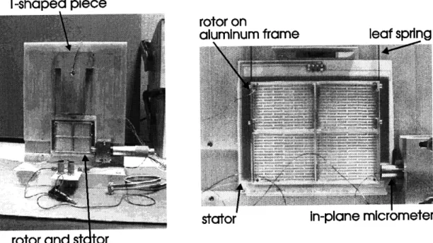
The rotor and stator plates were mounted vertically, like two opposite walls of a room. Because of the vertical mount, the effect of gravity on the motor was like the effect on a pendulum. The stator was attached by adhesive to a thick vertical insulating slab of G-10 (9.15"x8"x 1"), which rested on a heavy horizontal aluminum base (6"x8"xl"). The rotor was first attached to a light aluminum mounting frame by adhesive, then suspended from a T-shaped aluminum piece by two stainless steel leaf springs, designed to allow in-plane motion as shown in Figure 3.4. The springs were designed to be very flexible in the in-plane direction, so they would not exert much force on the
motor--the primary external force on the rotor was gravity. In the first half of the project, 0.002" thick springs were used. However, these were so easily bent out of shape that it was difficult to align the rotor. Later, 0.004" thick springs were found to be superior. Their greater stiffness made it easier for the rotor to be positioned very close to the stator. The T-shaped aluminum piece was supported using a kinematic mount with four degrees of freedom controlled by micrometers. By positioning the T-shaped piece, the rotor could also be positioned. Additionally, a micrometer was
mounted to control the in-plane motion of the rotor and is shown in Figure 3.4.
T-shaped piece
rotor on
aluminum
frame
leaf
spring
rotor and stdtor
Figure 3.4: Front view of motor mount (left), Close-up of rotor/stator (right) As mentioned above, the electrical connections to the rotor were minimized to reduce unnecessary mechanical influences. Two thin, 0.008" diameter wires were connected to the rotor and fastened to the heavy base for strain relief. The wires were allowed plenty of extra length to minimize their mechanical effect on the rotor. The rotor, its aluminum mounting frame, and the tape used to bind the rotor to the frame weighed 8.9 g.
Both the heavy metal base and the T-shaped aluminum piece were grounded. The
aluminum frame, which was shorted to the T-shaped piece via the springs, thus formed the ground plane for the rotor. The entire setup was placed on a regular tabletop.
3.3 Rotor alignment
It was important for the rotor to be positioned parallel to the stator so that 1) the two plates were parallel to each other with a uniform gap and 2) the electrodes on those plates were parallel. A small rotor-stator gap was desirable, because it would increase the rotor-stator capacitances,
producing greater forces and larger position signals. However, contact between the rotor and stator was undesirable because it would cause mechanical friction and electrical shorting. The rotor was positioned using micrometers to control the kinematic mount described above.
Chapter 3: Experimental Actuator
Two methods were used to gauge the uniformity of the rotor-stator gap: 1) visual
inspection by shining a light through the gap and observing how much light emerged from the slit and 2) observing the amount of mechanical damping caused by friction between the plates (any observable damping indicated contact between the plates). Using these two methods, the rotor was brought as close and as parallel to the stator as possible without touching it. The micrometers were then adjusted by a known amount to change the gap. After the gap was made as uniform as possible, the lower edge of the rotor was aligned to the visual alignment marks shown in Figure 3.1. This ensured that the rotor and stator electrodes were parallel.
The shape of the rotor and stator plates affected the alignment. Ideally, the rotor and stator planes would have been perfectly flat. Initially, there were some problems, because both the rotor and stator were actually slightly concave. This happened because the glue (photo mount spray adhesive) holding the rotor and stator to their mounts was not strong enough, so the edges peeled away slightly. The peeling was most noticeable along the upper and lower edges of the stator and rotor. Because of this warping, the perimeters of the rotor and stator were closer together than the centers. This restricted how close the rotor and stator could be aligned without touching.
However, later the rotor and stator were both remounted using doubled-sided masking tape, which improved the flatness. The glue probably didn't work because it was too old, not because the type of glue was inherently weak. Taussig had previously used the glue successfully on an earlier generation of the motor model. In addition, the aluminum frame that the rotor was mounted on was not perfectly flat, also affecting the rotor flatness.
3.4 Measuring the rotor-stator gap
Since the rotor and stator were not perfectly aligned, no single number could represent the gap, which varied across the plane. Also, in this motor setup, there was no good way of finding an absolute average gap measurement. The absolute gap was roughly estimated by sliding a piece of shim stock of known thickness into the gap without disturbing the rotor. Using this method, the smallest gap achieved without contact was roughly 0.005". However, this method only estimated the gap around the upper and lower edges of the rotor. During initial experiments, when both rotor and stator were concave, the center gap was roughly 0.012", even though the gap around the perimeter was around 0.005". Later, when a flatter rotor and stator were achieved, the overall gap was more uniform.
Although the absolute gap could not be measured accurately, the relative gap was easily measured. The gap measurements that follow refer to a relative gap setting, using an initial gap position as a reference. Because the stator was fixed, measuring the relative gap was equivalent to measuring the rotor position. As mentioned earlier, gap settings could be dialed into the
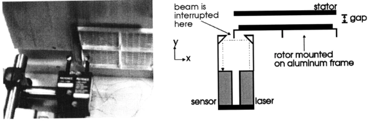
micrometers of the rotor mount. To test the accuracy of these dialed-in gap settings, a beam-interrupt device was used to measure the position of the rotor. Figure 3.5 shows the setup of the device.
beam is sttor
interrupted e
her(
L
Figure 3.5: Beam-interrupt device setup
The device worked by emitting a laser beam, then measuring how much of this beam was interrupted by an object in its path. The change in the beam's area corresponded to a change in position of the object. In this case, the beam was interrupted by a piece of metal on the rotor's aluminum frame. This metal piece was orthogonal to the beam and to the plane of the rotor, as shown in Figure 3.5. The dotted line in the figure represents the laser beam. As the gap increased, the rotor moved out-of-plane, and more of the beam was blocked. Using this
beam-interrupt device, an experiment was performed to test the accuracy of the dialed-in gap settings. During this experiment, the rotor was allowed to hang freely from the springs, without touching any other object. The dialed-in gap settings were changed and the change in rotor position was
Chapter 3: Experimental Actuator
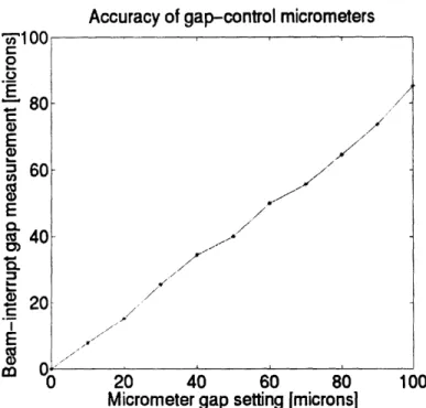
t.,-measured using the beam-interrupt device. The results are shown in Figure 3.6
Accuracy of gap-control micrometers
' t IUU r E 80 E 0 E r_ ' E 8 l " "0 20 40 60 80 100
Micrometer gap setting [microns]
Figure 3.6: Rotor's actual out-of-plane position compared to dialed-in setting
The two measurements should have yielded the same results, leading to a unity slope in Figure 3.6. However, Figure 3.6 shows that the beam-interrupt measurements were smaller than expected from the dialed-in settings. One reason for the discrepancy may be that the beam-interrupt device was not calibrated properly. Also, the rotor was connected to the micrometers by thin leaf springs which were not perfectly rigid, and the rotor's position may not have exactly copied the micrometer adjustments.
3.5
High-voltage tests
Although no high-voltage actuation experiments were conducted during this thesis, initial high-voltage tests were performed to make sure the motor parts could withstand the high voltages necessary to move them.
The rotor and stator were tested separately. To test the rotor, one trace pattern was grounded, while the other pattern was slowly raised to 475 V using a high-voltage power supply. The power supply was used in its constant current mode, with the current limit set as low as possible (10 mA). The stator was tested in a similar fashion: four of the five stator conductors were grounded while the remaining conductor (either an electrode pattern or the ground plane)
Chapter 3: Experimental Actuator
/i f 7J / 7 7 i /
/7-was slowly raised to 475 V. This was repeated for all five separate conductors on the stator. Figure 3.7a shows the initial test setup.
HOh voNage High votage
I
I
one pIase I
o-re
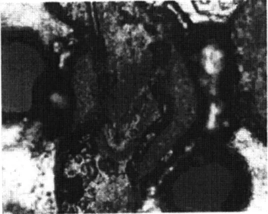
PhowFigure 3.7a: Initial high-voltage test Figure 3.7b: Revised high-voltage test In these tests, several stator boards were destroyed when shorting occurred between the drive electrodes. The shorting usually occurred around 200-300 V. Figure 3.8 shows a close-up of the damage to one of the stator boards. The area shown in the figure is roughly 0.020"x0.025". The traces near the short had evaporated or melted away! It is likely that the power supply was not able to limit the current quickly enough, so the damage occurred.
These failures suggested that the stator and rotor might have been dirty. Both the stator and rotor were then cleaned in an ultrasonic acetone bath for about fifteen minutes and dried with compressed air. Then they were retested with a revised procedure, depicted in Figure 3.7b. A 43 MO + 1 MO resistor was placed in series to prevent further damage. The current was monitored with an ammeter as the voltage was slowly raised to 475 V. If shorting had occurred, there would have been a noticeable increase in current, but no such jump was observed. Both the stator and rotor passed this high-voltage test after they had been cleaned. Also, another test was run with only the 1 MR resistor in series. The rotor and stator were also able to withstand high voltages
under these conditions.
Figure 3.8: Close-up of melted traces on stator during high-voltage testing All of these tests were performed on the rotor and stator when they were unmounted. Because of the particular mechanical setup, gaps less than 0.005" would be difficult to achieve without having some contact between rotor and stator. Smaller gaps (< 0.005") would be risky, because contact could easily occur if the setup were jostled, and because 400 V applied across 0.005" is already past the breakdown voltage of air (-3x10⁶ V/m). For 400 V, the distance at which breakdown occurs is 0.00525". In this thesis, the motor was not actually run at high voltages, but for high voltage operation, gaps should be kept around 0.01" or larger, to avoid air breakdown.
4.0 Position-sensing circuitry
4.1 Overview
Electronics were designed and built to implement the position-sensing method described earlier in Section 2.1.2. The electronics are shown as part of the system diagram in Figure 4.1. In
Figure 4.1: System block diagram; position-sensing circuitry shaded
this position-sensing method, the position information is encoded using AM modulation as the amplitude of a carrier (dither) wave. In order to use the Ed/Enorm and Eq/Enorm formulas
(Equations 2-3, 2-4, 2-11), the Vxi signals must be found by demodulating the raw stator output (Vx). One way to extract the Vxi signals is depicted in Figure 4.2.
^ _
Inpu
Vx
utput
Vxi
Pre-amp Bandpass Rectifier Lowpass Post-amp
filter filter
Figure 4.2: Demodulation scheme
In Figure 4.2, one demodulation channel is shown. Since the motor had four stator phases, each of which had to be demodulated for two frequencies, a total of eight demodulation channels were needed, one for each Vxi signal (x=A,B,C, or D; i=l or 2). Four channels were designed to handle one dither frequency, and the other four channels handled the remaining dither frequency. These were assembled on a protoboard using Wire-Wrap. The schematic diagrams for the
demodulation circuitry are shown in Appendix C.
Section 4.2 describes how the dither frequencies were chosen. Sections 4.3, 4.4, and 4.5,
discuss the bandpass filter, rectifier, and lowpass filter respectively. Finally, Section 4.6 evaluates the overall demodulator performance.
4.2 Choosing dither frequencies
Three criteria were used to choose the two dither frequencies:
1) the frequencies had to be high enough to resolve the motor's motion in time, 2) the frequencies had to be sufficiently far apart so that the bandpass filter could
distinguish them, and
3) the bandpass filter and other demodulators components had to be able to work at those frequencies.
The DSP that would perform the control algorithm was capable of sampling the position information at up to 10 kHz. Following a rule of thumb for a noise-limited digital servo, the control loop was estimated to have bandwidth around 1 kHz, and the motor's motion would fall within this bandwidth. Since the dither frequencies control the time-resolution of the position signal, they had to be much higher than 10 kHz, the sampling rate. The higher the dither frequencies, the greater the time-resolution of the signal.
However, the choice of dither frequency was also limited by the decision to use switched-capacitor bandpass filters in the first stage. The best filter readily available had a maximum center frequency around 100 kHz while maintaining a Q-20.
Finally, if the dither frequencies were too close together, the bandpass filters would not be able to select a single frequency--information about both frequencies would overlap into all demodulation channels.
Based on these criteria, dither frequencies f1=70 kHz and f2=95 kHz were chosen. In
addition, these were close to the frequencies used by Taussig in his initial, successful experiments with this position-sensing technique.
4.3 Bandpass filter
4.3.1 Design criteria
The ideal bandpass filter for this application would have had a perfectly flat passband,
centered about one of the dither frequencies. More design criteria can be uncovered by examining
a hypothetical input to the bandpass filter:
A A
= [sin(oclt) + M cos(Wcl - m)t - 2cos(cl + 0m)t
A . M M.
+ [sin L(Oc2t) + sin (Oc2 Om)t + sin (c2 + Om)t
where Vx=signal from single stator phase x
oci=dither frequencies (oci/2n - 70-100 kHz)
i=dither frequency index (i=1 or 2)
(Om=modulation envelope (position signal) frequency (Om/2 t < 1 kHz)
A=amplitude
M=percent modulation (0o M < 1, corresponding to a range of 0% to 100%)
Suppose we want to pass the terms dealing with dither frequency 1. The bandpass filter
must have a wide enough passband to pass cos( cl +/- om), while still attenuating the signal
components from the other dither frequency. However, since no filter will be perfectly flat, it is also important for the bandpass filter to be symmetrical about the center frequency. A fast transient response is also desirable. Since the design is for a maximum modulation frequency of 1 kHz, the maximum motor speed the circuit can handle is (1 kHz)(0.040")- 1 m/s. If the motor were to move faster than 1 m/s, the motion would be beyond the bandwidth of the circuit.
4.3.2 Bandpass implementation: LMF100
Initially, a Sallen-Key design was investigated for the bandpass filter, but a switched-capacitor filter was later chosen because of time constraints on the thesis. The advantages of a switched-capacitor filter are that the bandpass center frequency can be easily changed by altering the clock frequency, and that the filter is easy to use. However, this type of filter does have clock noise which would not exist in a Sallen-Key design. [7] Many types of switched-capacitor filters
were reviewed, but the LMF100 was chosen because it could realize filters with high center frequencies (- 100 kHz) and relatively high Q's compared with other switched-capacitor filters. In general, a high Q was desired, because the higher the Q, the more the bandpass filter would be able
to selectively pass a single dither frequency with minimal overlap from the neighboring dither signal. However, if the passband region were too narrow (< 20m), the gain at frequencies Oci +/-(0m might be too low.
4.3.3 Type of filter: Butterworth
Once the LMF 100 was chosen and passed preliminary tests, the type of bandpass filter was chosen. The LMF100 is capable of implementing Butterworth, Chebyshev, Bessel, and other classical filters. Although a Chebyshev filter was considered, the Butterworth design was used because it was simpler to implement and did not have passband ripples (which might distort the modulation envelope). Although the Butterworth filter had a slower time-domain response than the Chebyshev, it was still faster than the Bessel filter and so provided a compromise between the Chebyshev and Bessel. The bandpass filter is shown below as it was used during experiments.
R1B lu -- --- -- --
---R3A A A,,
R3A LPa LPb 0 'R3B
BPa BPb --- out
From [,Frm -INVa N/APiHPa NAP!HPb INVb i vR2B
pre-amplifier RV1 Sla Sib1
SSa/b AGND +8V-- VA+ VA- - - 8V SVD+ VD-4 S - - - Sh 50!100 T---: Cb CLKa CLKbf-
4
0 LMF100 0 DSTM1 4 -4 ---- --- --- - ---- _ -- --- --- ---.Figure 4.3: Bandpass filter: implemented circuit
The LMF100 was used in mode lb to create two cascaded 2nd-order Butterworth bandpass filters having the following total transfer function:
-(-R3a)(O)i) (-R3b)
rOi)
H(s) = a a Rb Qb (4 - 2)
S2 +02 S2+ (2Oi S+0)2
0oi = 2rf0oi = 27CfCLK_i 5 (4-3)
fol R
foi R3(a b)2 (4-4)
Qa, b (-3 dB bandwidth of output) R2(a, b)
where Rla, R2a, R3a=external resistors for 1st stage (2nd-order Butterworth filter)
Rib, R2b, R3b=external resistors for 2nd stage (2nd-order Butterworth filter)
Qa=Quality factor for 1st filter stage Qb=Quality factor for 2nd filter stage
ooi=2itfi=bandpass center frequency (same for both stages) fclk_i=clock frequency input to LMF100 (same for both stages) i=dither frequency index
This filter could have been improved. It was later realized that the LMF100 could have been used in mode 3, which would have allowed two internal clock signals to be created from one external clock signal, using a few additional external components. However, this option was not pursued at the time of design. Using mode 3 would have been better, because it would have easily allowed a 4th-order Butterworth filter to be implemented without extra equipment. A 4th-order filter would have had a flatter passband and steeper transition region. However, since the Butterworth filter has a maximally flat passband in any case, this improvement may not be significant.
4.3.4 Clock and dither signal sources
Including the two dither signals (mci) and two LMF 100 clock signals (fclk_i), four separate
periodic signals had to be generated. However, only two signal generators were required to produce all four signals. This was possible because each clock frequency is related to its
corresponding bandpass center frequency by a factor of -35.4 (Equation 4-3). To take advantage of this, an Altera EPLD (Erasable Programmable Logic Device) was programmed to perform a divide-by-35.3 function. If the EPLD received an input square-wave of frequency f, it would output two square-waves at frequencies: f/212 and f/6. The program for the EPLD was written by
Carl Taussig and is listed in Appendix D. Two such EPLD's were used, one for each dither frequency. In summary, two signal generators fed a high frequency signal to two EPLD's, each of which produced a dither and clock signal. The signals produced by the EPLD's were square waves.
Problems with the clock and dither signal sources
Ideally, the dither signal frequency (Oci) and bandpass center frequency (oOi) should have been exactly the same. In reality, there were several issues involving the clock signals which affected the bandpass center frequency. These problems suggest the dangers of having a passband that is too narrow--it is too difficult to align the bandpass center frequency and dither frequency.
First, since 212/6-35.3, this was an approximation to 35.4 and would result in some error: the dither signal frequency and bandpass center frequency might not be the same.
Second, it was also found that the dither frequency and bandpass center frequency might differ by several kHz, depending on the external components to the LMF100. These components were chosen to minimize the difference between the dither frequency generated by the EPLD and the center of the bandpass.
Third, the fclk_i/f0i ratio shown in Equation 4-3 was slightly different, depending on fclk_i.
In the LMF100 data sheets, a graph is given showing the ratio's dependence. In early experiments, it was determined that for f02=95 kHz, it would be better to use a ratio of 36 instead of 35.3, which
agreed with the information in the LMF 100 data sheet, which is shown in Appendix E. However, later in the thesis, measurements were taken which showed that a ratio of 35.3 was better for producing a bandpass center frequency of 95 kHz. This issue remains unresolved.
Fourth, although each chip was slightly different, with a slightly different fclk/f0i ratio, all four 70 kHz LMF100 filters received the same fclk_1, and all four 95 kHz filters received fclk_2* This was another reason that the bandpass center frequencies were not precisely aligned to the dither frequencies.
The above difficulties show why it is dangerous to have a bandpass filter with too narrow a passband. It is difficult to precisely place each filter's f0i exactly at the same frequency as the
corresponding dither signal. A narrow passband which is not at the exactly same frequency as the dither signal may miss the signal entirely and attenuate it instead.
4.3.5 Filter parameters and performance
After some experimentation, the following values were chosen to yield two cascaded
2nd-order filters, each with a Q of 10. The overall passband gain was 1 dB and overall Q was about 17.
The components in Table 1 refer to Figure 4.2 and Equations 4-2 through 4-4.
Table 1: Component values for LMF100 bandpass filter
Component fc Resistance Name [kHz] [kW] Ria 70 34.8 Ria 95 42.2 Rlb 70; 95 50 (variable) R2a 70; 95 8.25 R2b 70; 95 8.25 R3a 70; 95 61.9 R3b 70; 95 61.9
In initial experiments, it was found that when the same filter IC was operated at different clock frequencies (all other parameters held constant), different gains resulted. For this reason, the Ria resistors had different values, depending on fc. A variable resistor was used for Rib to adjust for differences between chips. Figure 4.4 below shows the experimentally measured transfer
functions for two different bandpass filters, one with fcl=6 7 kHz, and one with fc2=95 kHz. 67
kHz was used instead of 70 kHz because of a restriction on fcnk_1 due to equipment. Rlb= 39.4 kW
was used for the filter at fc1=67 kHz, and Rib = 35.0 kM was used for the filter at fc2=95 kHz.
Using these components, the expected transfer functions from Equations 4-2 through 4-4 were
calculated and are shown in Figure 4.5. Y-0. 01 s , I I I I 11111I ! Iii I I I I I I I I I l tii I I t I tll I I t I tit I I ! 11111 I I I 111I I I i i IIlt I I I I lII I I I tlIt I i I I I Iit I I t t t t I I 1 1 1 I! I I I I i ll! i I iZr , j __ ,rt !!t i4~ 111111l I I 11111 " ; I ; I- llt I I I I I I II I I I I I| II . I i i ll i I I I i ri I I I ii IIi i I Il lii i 1 iI il S I lItI I! I I Il t I I 11111 I ! t111 I • I 11i 11 I I I I i t 1 I ! I 1 I1I 1 I I I I i Iii I I I t I I I I 11111 L.Og ix o04k 0F0IR: A nPPP'WQli I1 P8 10.0 do -70.4 P34 Y Y -e. Iam do 1 I I I tI il I I I liii! 1 ! :1 I 11111 I 1 1 h! I.Ih I I I I 1 111 .. :I I I Ii l Iii 1 I t I: : : I I I1 I tI _1::: 1 I 1 Ilit I I I I i lt!!i: : : r c:ii : I I:: 111: 111t lll , ; I I i I t t I i I III I i SI I liii S I I I ilt I I I I I *I. . i i iil /i' I I I I I I1 ii I I I I I I/ . I I I I: 1 I I ! I l Ii I I I t I IIlt 1 I I .. I I I i I i i I 1 11 SI I I tll i r I I i I1 I !I i I I I It I l IIIIII itII I I 1 I 1 I I11 1111 I1 LOg :Z
Figure 4.4a: Experimental bandpass transfer function with fc=67 kHz
2 cascaded 2-pole Butterworth using LMF100: 67 kHz 10 - 1 0 . " -20 . . -40 -50 - 60 ... ... _7n , ,47 10 Frequency [Hz]
Figure 4.5a: Expected bandpass transfer function with fc=67 kHz
Figure 4.4b: Experimental bandpass transfer function with fc=95 kHz
2 cascaded 2-pole Butterworth using LM F100: 95 kHz
10 Frequency [Hz]
Figure 4.5b: Expected bandpass transfer function with f,=95 kHz As can be seen from the figures, experimental gain and peak sharpness were lower than expected. For both experimental filters, the peak gain was roughly 5 dB greater than the gain at the non-peak dither frequency.
Figure 4.6 shows close-ups of the passband peaks for the experimental filters. (Note that the horizontal axes are on different scales.) Unfortunately, these passband regions were not very
Chapter 4: Position-sensing circuitry
414 do AIl.l, WVIO PrMQ 10.0 10.0 /Div0 I I i iii S I 1 I il o -70. Fxd Y 1k
I
! ii
i
-- , .. .. . . . -_ _.° " . ... - -A- ; .. tO1 Skflat. For both filters, the passband is only flat for about 2 kHz. :.:-i. I il | I i i :1 -1-I ± 10. 10. /01 c, ii'
i-i
C:
I I 0 ... - - -. - - - -• 4.o
-i
I
1-L rFigure 4.6a: Experimental bandpass peak Figure 4.6b: Experimental bandpass peak
with fc=67 kHz with fc=95 kHz
In future, a 4th-order filter should be implemented in mode 3, because only a few more external components would be needed to implement it, and it would improve performance. Using a 4th-order Butterworth filter would increase the passband flatness and transition-region steepness slightly, coming closer to the ideal filter. From Figure 4.5, the cascaded 2nd order filters yield a 3 dB passband of roughly 4 kHz.
Finally, offset voltage was another important element of the bandpass filter. Ideally, the output of the bandpass filter would have no DC component, however, in reality the output was offset by around -0.1 V. This output offset was independent of the input offset or input amplitude. Since the signal range was expected to have an amplitude of around 2 V, the offset from the bandpass filter was not expected to cause problems.
4.4 Absolute value circuit: implemented using multiplier
Initially, a standard full-wave rectifier, using three diodes and an op-amp, was considered. However, for convenience, a multiplier IC (AD734) was used instead, shown below in Figure 4.6. Using the multiplier, the function X2/D was implemented. Although this was not an absolute value function, it did ensure that the signal became positive, so that the position signal would be preserved after going through the lowpass filter. The value of the denominator, D, was controlled by external resistors. The multiplier chip was tested by feeding it a +/- 4V square wave, which was transformed into a single DC voltage -7V. Thus, the experimental value of D was -2.8, which was close to the expected value of D=3 that the external resistors had been chosen to create. D was
Si 34 lu.V 10.0 /DLv do -70.0
!i
Si
iiiiI
rc ---I I--r 3 I L c I -r. 1CI
I
I
r Iii1-t
r I I I -70. O- - 76k PXd Y 210k L X1 Iiii I~ii ~i c- i..-Clj -I I -I la r"j-i
,._ ,. WAMS Y~ LP -- I--L ~CI ~i~~ rIv ~E r rT r ur I,Crapter 4,: OSiLtlon-s nsing t)yIcut
I-- --~ICc~-' '
'-P 1 i
I
maintained at this value through the rest of the project. There were some periodic spikes in the output, but for the most part it performed adequately. This experiment was tried at various frequencies (5 kHz, 100 kHz) and seemed to work just as well at either frequency.
in
0
Ri
out
Figure 4.7: Multiplier circuit diagram
4.5
Lowpass filter
The criteria for the lowpass filter were less stringent than those for the bandpass filter. The lowpass filter needed to preserve low-frequency (< 5 kHz) signals while attenuating the high-frequency dither signals (70-95 kHz). However, it was also important for the passband to be flat in the region where the position signal would be expected (< 1 kHz).
A switched-capacitor filter was also used to implement the lowpass filter. The LMF40, a 4th-order Butterworth lowpass filter, was chosen for ease of use. An advantage of this IC was that no external clock signal was needed to set the lowpass filter's cutoff frequency. Instead, external components could be used to set an internal clock frequency. There was no way to control the gain on the LMF40, so a standard non-inverting op-amp was placed after the lowpass filter in each demodulation channel to control the gain.
External components (R=2.61 k4 C=680 pF) were chosen to yield an expected cutoff frequency of 8.2 kHz, since the experimental cutoff frequency was found to be lower than
expected. Figure 4.8 shows a typical lowpass transfer function. XaWS9 e-5 FRE 10. 10. /01 a.7 HZ S.0271 d8 O o ! l 1, 1 1; 1 1 ,,111. 11;;' 411111 1 1, ! 11!11 :oil 1 1 ...r I llll I . .l.l I 4 ,,lllll~c~t 1 I ... rIi t t I 1.I 11 id I I i 01111IIIII tlil~it td~ftlf 1ff(f~t 1 1 1 filltl~l~ 0 I 1 a aaIIII I it, I 1 11111
I II III I I i t tII I MI III I It I 111M I t I 1jlt I Iiili I I IlII. a a aaa 4 a It I alalaI
I I ~ ~ ~ ~ ~ It 1. 11 III lI 1111111 III # .. 1 I 1III It 1 i :.I I 11111 III
M
!. U I 11 !II I 1 I11I I IIIIII 1!i I I I I -I I I4N I
$I aalaI 11 l ai1i I I a a ltta .t tl, .I I lala a a l a I lt ll
4{ 4 4:taa ... I:tiH ~il liltaa
al i aal a a aaaaaa ai a aaaaiifa a a ;iaaiai ai a aaaa
at ailatll a a aaaaaal a a !a!aIai 7:1 a ! aaall a al laa!!t
..-L-LJ.Z 11 ....t4..L! III!i -i -LMItI 7'I::I7tIl : I!11 i a aaaaal i a a aaaa ll a:Ii "aaa a a laaitl aI ai a l
a a aalaall a a aaaaal a I aiaaaa a a aaaaaa al a aaaaa
-70*0 1 I I IIt l I I iiiil 1il4i 1 1 i :i! l I4 iilli
Fxd Y i L9g Hz o
Figure 4.8: Experimental lowpass transfer function
This figure shows that the passband region is not flat. Around 200 Hz - 1100 Hz, there is a
5 dB dip before the main knee around 5 kHz. This is bad, because it means that the output amplitude depends on the frequency of the position signal, possibly distorting the position signal. In future, this might be improved by moving the cutoff frequency up by 15 or 20 kHz or by using a different kind of lowpass filter.
4.6 Overall demodulator performance
Despite the fact that the demodulator was not optimized, it still performed its basic function. A few experiments were performed on the overall demodulator to explore its
characteristics. In particular, the dependence of the output on the input amplitude, frequency, and percent modulation were investigated. Also, frequency spectra were taken at various stages as a known signal passed through the demodulator, giving noise information.
Theoretically, if the input signal is as follows:
V V
V(t) = PP[1 + Msin(omt)]sin (Ocit) + -[1 + Mcos(Omt)]sin(Oc2t) (4-5)
2 M2f(~tIS~lCct
then the final demodulator output signal should be
K + Msin(cit) if i=1
Vxi(t) = (4-6)
K [+ Mcos(Oc2t)] if i=2
where i=dither frequency index x=stator phase index
K=constant gain (depends on gain of each stage) Vpp=input amplitude
M=percent modulation (o s M 1 , which corresponds to a range of 0% to 100%)
1
ci=2fi=dither frequency (70-95 kHz) oam=2nfm=modulation frequency (< 1 kHz)
The theoretical output (Equation 4-6) takes into account the X2/D function, but assumes a perfect bandpass and perfect lowpass filter. In Equation 4-6, the value of i depends on which dither signal the demodulation channel is tuned for, fl or f2. Experimentally, the output was different from Equation 4-6 because of noise, saturation at various stages, and imperfect filters. In addition, Equation 4-5 only represents a hypothetical input, with asinusoidal modulation and sinusoidal dither signal.
4.6.1 Varying the input amplitude
In this experiment, an unmodulated (M=O) 95 kHz square wave with no offset was fed to the demodulator, producing a DC value at the output. A square wave was chosen, because the
dither signals produced by the Altera EPLD were square waves. The output level was observed as the input peak-to-peak amplitude (Vpp=Vmax-Vmin) was varied. From Equations 4-5 and 4-6, we would expect a graph of the output level to input amplitude to resemble an Vpp2function. Figure
4.9 shows the relationship between input peak-to-peak amplitude and output level. 5 1 0
joS
7 Ai i/,.
/ 7 / ' 0 2 4 6 10 12 14VPPeak-to-peak amplitude of inputsquare wave [VI
Figure 4.9 Varying the input amplitude to the demodulator
When the peak-to-peak input amplitude nears 10 V, the output starts leveling off. This was probably due to saturation of the signal at some stage of the demodulator, most likely the multiplier. Each stage was powered by +/- 8V power supplies and could only handle signals within this range. For example, when an input signal with Vpp=10 V passes through the multiplier, the maximum predicted voltage is roughly 52/2.8 - 8.9 V. This is higher than the multiplier can handle, so it saturates, and the signal is deformed.
4.6.2 Varying the input modulation frequency
Ideally, the output should not depend on the input modulation frequency, as long as this frequency is within a reasonable range (< 5 kHz). In this experiment, the input modulation frequency ((om) was changed while all other input parameters were held constant. Referring back to Equation 4-5, the input signal was a modulated 98 kHz sine wave with M-1, Vpp=8 V. The following graph shows the dependence of the output amplitude on the input modulation