THE EFFECT OF IMPLANTS ON THE
STRUCTURAL INTEGRITY OF GRAPHITE/EPOXY
LAMINATES
by
Laura Ann Kozel
B.S. Aerospace Engineering, The Ohio State University (1989)
Submitted to the Department of Aeronautics and Astronautics in Partial Fulfillment of the Requirements for the Degree of
MASTER OF SCIENCE at the
MASSACHUSETTS INSTITUTE OF TECHNOLOGY
September 1992
Copyright @ Massachusetts Institute of Technology, 1992. All rights reserved. Signature of Author
Department of Aeronauj and Astronautics
T1 I Ir9Q 1009 I ' uJ Lly £.JLJ .L.J.J Certified by Accepted by MASSACHUSETTS INSTITUTI
'SEP 22
1992
U~bnrv~--Professor Michael J. Graves Thesis Supervisor
IV
Professor Harold Y. Wachman Chairman, Department Graduate Committee EThe Effect of Implants on the
Structural Integrity of Graphite/Epoxy Laminates by
Laura Ann Kozel
Submitted to the Department of Aeronautics and Astronautics on July 28, 1992, in partial fulfillment of the requirements for the Degree of
Master of Science. ABSTRACT
Experiments were performed to study the structural integrity of graphite/epoxy laminates with embedded optical fibers, circuit chips, piezoceramic actuators (PZA) and teflon. Embedded devices are characteristic of the smart structure concept where a structure monitors its own structural integrity and can adapt to external disturbances. The devices were embedded parallel to the loading direction into four different laminate configurations which had 10/80/10%, 25/50/25%, 40/50/10% and 0/100/0% of 0*/45*/90* plies. Uniaxial tensile testing was performed to determine the effects of the implants on the ultimate tensile stress, failure mode, and to determine at what loading damage initiated and if initial damage occurred at the implant. The implants were placed in cut out sections of the laminate with the exception of the chip and optical fiber implants, which were also placed directly into the laminate. All specimens were x-rayed and both failed and partially loaded specimens were sectioned and examined for delaminations or matrix cracking at the implant. Results indicated that the implants degraded the ultimate tensile stress up to 16% in the layup where 0O plies were cut to embed the devices. The implants had the least affect on ultimate stress when they were in layups with high percentages of ±45* plies. Implants demonstrated the ability to significantly reduce the laminate ultimate stress but were not necessarily the failure initiation site. Matrix cracking was observed in all tested specimens. Delamination at the side of the PZA implant embedded in a 100% ±45* laminate was also observed. There was no significant difference in ultimate stress for specimens with the chip implant placed in a cut area or placed directly into the laminate; however, placing the chip directly into the laminate appeared to prevent failure at the implant and had little effect on failure mode. Teflon implants degraded the ultimate stress in a manner comparable to the actual chip and PZA implants. The optical fibers degraded the ultimate stress up to 12% but did not appear to affect the failure mode of the laminates and no delamination was observed at the implant.
Thesis Supervisor: Michael J. Graves
Title: Assistant Professor, Department of Aeronautics and Astronautics, Massachusetts Institute of Technology
Acknowledgments
My work at MIT would not have been possible without the extemely generous financial support of my managers at the GE Aircraft Engine Company. I sincerely appreciate the time off for classes and the months off to work on my thesis (although some people would argue my absence was a blessing!). Thank you Paul LoPiccolo for supporting me during my time at MIT even when I was acting crazy. I appreciated the visits in the lab (especially when they were accompanied by food!) and your continued offers to help me even after you smashed your bum into the caul plate! I hope you will always treasure the picture of the geek at the milling machine. My advisor, Michael Graves, deserves a special thank you for his guidance and especially for making sure there were no spaces before the paragraph symbols in my thesis! I also enjoyed working with a great set of Professors, Administrators and Research Associates including Paul Lagace, Hugh McManus, John Dugundji,
Queen Ping Lee, Debbie Bowser and Al Supple!
Good-Bye!
* My favorite car ever, the 1989 black Acura Integra with moonroof and awesome interior (Merry X-Mas)
* Late Friday night strain gaging * Splinters in everything
* Dirt encrusted hands from the milling machine
* Spending an entire day cutting apart strips of 10 coupons that stuck together during a bond cure
* The computer mezzanine (I will never listen to 101.7!) Hello!
* Friday and Saturday nights * Daylight
* Learning how to play the piano * Building the perfect body
* Life outside
Some Things Never Change (and some people take longer to graduate than others):
My friendships with Narendra, Wilson, Steve, Mak, Hiroto, Mary, Ed, Hary, Aaron, Jeff, Stacy, Malee, Elizabeth, Kerry, Kim, and Amy. All the other UROPers aren't so bad either!!!
Foreword
This work was performed in the Technology Laboratory for Advanced Composites (TELAC) of the Department of Aeronautics and Astronautics at the Massachusetts Institute of Technology. This work was sponsored by the GE Aircraft Engine Company and Leaders for Manufacturing.
Table of Contents
Chapter
Page
1. Introduction ... ... 22
2. Background... ... ... 27
2.1 Optical Fiber Implant Research... 27
2.2 Piezoceramic Implant Research ... ... 31
2.3 Circuit Chip Implant Research ... 31
3. Experimental Procedure ... ... 33
3.1 Experimental Approach... ... 33
3.2 Manufacturing Procedure of Tensile Coupons ... 44
3.2.1 Implanting Circuit Chips... 49
3.2.2 Implanting the Piezoceramic ... 52
3.2.3 Implanting the Optical Fibers... 56
3.2.4 Implanting Teflon ... 58
3.2.5 Specimen Coding ... ... 58
3.2.6 Curing Procedure... 59
3.2.7 Cutting Tensile Coupons ... 63
3.2.8 Manufacture and Bonding of Loading Tabs ... 64
3.3 Instrum entation ... 67
3.4 Testing Procedure ... 70
4. Experim ental Results... 75
Chapter
Page
4.2 Ultimate Stress Results...76
4.2.1 Ultimate Stresses for Implanted Specimens with a Layup 1, [0/(±45)2/90/(±45)2]s, Configuration ... 82
4.2.2 Ultimate Stresses for Implanted Specimens with a Layup 2, [0/±45/9012s, Configuration ... 82
4.2.3 Ultimate Stresses for Implanted Specimens with a Layup 3, [45/0/-45/0/90/-45/0/-45/0/45]s, Configuration ... ...83
4.2.4 Peak Stresses for Implanted Specimens with a Layup 4, [±4514s, Configuration ... 84
4.3 Stress-Strain Curve Results ... 84
4.3.1 Stress-Strain Curves for Virgin Specimens ... 85
4.3.2 Stress-Strain Curves for Specimens with a Layup 1, [0/(±45)2/90/(±45)2]s, Configuration ... 90
4.3.3 Stress-Strain Curves for Specimens with a Layup 2, [0/±45/90]2s, Configuration... 90
4.3.4 Stress-Strain Curves for Specimens with a Layup 3, [45/0/-45/0/90/-45/0/-45/0/45]s, Configuration ... ... 99
4.3.5 Stress-Strain Curves for Specimens with a Layup 4, [±4 514s, Configuration ... 105
4.4 Failure M odes ... ... 105
4.4.1 Layup 1, [0/(±45)2/90/(±45)2]s, Failure Modes ... 109
4.4.2 Layup 2, [0/±45/9012s, Failure Modes ... 115
4.4.3 Layup 3, [45/0/-45/0/90/-45/0/-45/0/45]s, Failure M odes ... 123
4.4.4 Layup 4, [±4 5]4s, "Failure" Modes...132
Chapter
4.5.1 X-Ray Damage Detection at Implants for
Specimens with a Layup 1, [0/(±45)2/90/(±45)2]s,
Configuration ... 135 4.5.2 X-Ray Damage Detection at Implants for
Specimens with a Layup 2, [0/±45/90128,
Configuration ... 135 4.5.3 X-Ray Damage Detection at Implants for
Specimens with a Layup 3,
[45/0/-45/0/90/-45/0/-45/0/45]s, Configuration ...143 4.5.4 X-Ray Damage Detection at Implants for
Specimens with a Layup 4, [±45]48,
Configuration, ... 143 4.6 Sectioning Results of Tensile Specimens ... 145
4.6.1 Sectioning Results for Specimens with Chip
Im plants ... ... 147 4.6.2 Sectioning Results for Specimens with PZA
Im plants ... 147 4.6.3 Sectioning Results for Specimens with Optical
Fiber Implants ... ... 52 4.6.4 Sectioning Results for Specimens with Teflon
Im plants ... ... 157 5. D iscussion ... 160
5.1 Prediction of Ultimate Stress Reduction and Overview of Results ... 160 5.2 Effect of Implants in Specimens with a Layup 1,
[0/(±45)2/90/(±45)2]s, Configuration...165 5.3 Effect of Implants in Specimens with a Layup 2,
[0/±45/90128, Configuration...168 5.4 Effect of Implants in Specimens with a Layup 3,
[45/0/-45/0/90/-45/0/-45/0/45]s, Configuration ... 173
5.5 Effect of Implants in Specimens with a Layup 4, [±4514s, Configuration ... 177
Chapter
Page
6. Conclusions and Recommendations...179
6.1 Conclusions...179 6.2 Recommendations ... 81 References ... .. 183 Appendix A Appendix Appendix Appendix Appendix E Appendix F Appendix G Thickness and Width Measurements of all Tested Specim ens ...187
Failure Stresses of All Tested Specimens ... 196
Stress-Strain Curves for Virgin Specimens ... 198
Stress-Strain Curves for Specimens with a Layup 1 [0/(±45)2/90/(±45)2]s, Configuration ...210
Stress-Strain Curves for Specimens with a Layup 2, [0/±45/9012s, Configuration ... 220
Stress-Strain Curves for Specimens with a Layup 3, [45/0/-45/O0/90/-45/0/-45/0/45]s,Configuration...240
Stress-Strain Curves for Specimens with a Layup 4, [±4514s, Configuration...250
List of Figures
Figure
Figure 3.1 Figure 3.2 Figure 3.3 Figure 3.4 Figure 3.5 Figure 3.6 Figure 3.7 Figure 3.8 Figure 3.9 Figure 3.10 Figure 3.11 Figure 3.12 Figure 3.13 Figure 3.14 Figure 3.15 Figure 4.1Page
Enlarged View of Micromet Integrated Dielectric
Circuit Chip and Lead Attachment... 37
Schematic of Piezoceramic Implant with Lead Wires Attached ... ... 40
Comparison of Implant Sizes... 43
Tensile Specim en ... 46
Creation of 450 and 90' Ply From Unidirectional Tape ... 47
Templates Used to Cut Holes in Graphite/Epoxy for Chip Implants ... 50
Sublaminate Approach to Implant Chips ... ... 51
Templates Used to Cut Holes in Graphite/Epoxy for PZA Im plants ... 54
Sublaminate Approach to Implant PZA ... 55
Placement of Optical Fibers in Graphite/Epoxy L am inate ... 57
Standard Plate Cure Set-Up ... 60
Standard Cure Cycle for AS4/3501-6 Graphite/Epoxy Laminates ... ... ... Coupon Thickness and Width Measurement Locations ... 65
Strain Gage Placement for Virgin Specimens ... 68
Strain Gage Placement for Specimens with Implants... 9
Stress-Strain Curves for Virgin Coupon 1V-E with a Layup 1, [0/(±45)2/90/(±45)2]s, Configuration Tested to Failure ... 86
Figure
Figure 4.2 Figure 4.3 Figure 4.4 Figure 4.5 Figure 4.6 Figure 4.7 Figure 4.8 Figure 4.9 Figure 4.10 Figure 4.11 Figure 4.12Stress-Strain Curves for Virgin Coupon 2V-A with a
Layup 2, [0/±45/90]2s, Configuration Teste&dto Failure...87 Stress-Strain Curves for Virgin Coupon 3V-B with a
Layup 3, [45/0/-45/0/90/-45/0/-45/0/45]s, Configuration
Tested to Failure ... 88 Stress-Strain Curves for Virgin Coupon 4V-A with a
Layup 4, [±4 5]4s, Configuration Tested to 100% of its
Peak Stress ... 89 Stress-Strain Curves for Coupon 10F-D with a Layup
1, [0/(±45)2/90/(±45)2]s, Configuration Tested to 95% of
its Ultimate Stress ... 91 Stress-Strain Curves for Coupon 1CHIP-D with a
Layup 1, [0/(±45)2/90/(±45)2]s, Configuration Tested to F ailure ... 92 Stress-Strain Curves for Coupon 1PZA-E with a
Layup 1, [0/(±45)2/90/(±45)2]s, Configuration Tested to 90% of its Ultimate Stress ... 93 Stress-Strain Curves for Coupon 20F-E with Optical
Fiber Placed Directly in Laminate with a Layup 2,
[0/±45/90]2s, Configuration Tested to Failure ... 94 Stress-Strain Curves for Coupon 2CHIP-A Tested to
Failure with Chip Placed in Cut Laminate with a
Layup 2, [0/±4 5/901]2s Configuration... 95 Stress-Strain Curves for Coupon 2PZA-E with a
Layup 2, [0/±4 5/9012s, Configuration Tested to 90% of its Ultimate Stress ... 96
Stress-Strain Curves for Coupon 2TC-C with a Layup 2, [0/±45/90128, Configuration Tested to 90% of its
Ultim ate Stress ... 97 Stress-Strain Curves for Coupon 2TP-E with a Layup
2, [0/±45/9012s, Configuration Tested to 95% of its
Figure
Figure 4.13 Figure 4.14 Figure 4.15 Figure 4.16 Figure 4.17 Figure 4.18 Figure 4.19 Figure 4.20 Figure 4.21 Figure 4.22 Figure 4.23 Figure 4.24Page
Stress-Strain Curves for Coupon 2CHIP-A Tested to 90% of its Ultimate Stress with Chip Placed Directly in Laminate with a Layup 2, [0/±45/9012s,
Configuration ... 100 Stress-Strain Curves for Coupon 20F-C Tested to 90% of its Ultimate Stress with Optical Fiber Placed in Cut
Laminate with a Layup 2, [0/±45/901]2s, Configuration...101
Stress-Strain Curves for Coupon 30F-E with a Layup 3, [45/0/-45/0/90/-45/0/-45/0/45]s, Configuration Tested
to Failure ... 102 Stress-Strain Curves for Coupon 3CHIP-E with a
Layup 3, [4 5/0/-4 5/0/90/-45/0/-45/0/4 5]s, Configuration
Tested to 95% of its Ultimate Strength ... 103 Stress-Strain Curves for Coupon 3PZA-D with a
Layup 3, [45/0/-45/0/90/-4 5/0/-4 5/0/4 5]s, Configuration
Tested to Failure...104 Stress-Strain Curves for Coupon 40F-D with a Layup 4, [±4 514s, Configuration Tested to 100% of its Peak
Stress ... 106 Stress-Strain Curves for Coupon 4CHIP-E with a
Layup 4, [±4514s, Configuration Tested to Failure ...107 Stress-Strain Curves for Coupon 4PZA-D with a
Layup 4, [±4514s, Configuration Tested to 100% of its Peak Stress ... 108 Nomenclature Describing Locations Around the
Implant ... 110 Photographs of Failure Modes of Virgin Specimens
with a Layup 1, [0/(±45)2/90/(±45)2]s, Configuration...111 Photograph and X-Ray of Coupon 1CHIP-C with a
Layup 1, [0/(±45)2/90/(±45)2]s, Configuration Tested to Failure ... 113 Photograph and X-Ray of Coupon 1PZA-E with a
Layup 1, [0/(±45)2/90/(±45)2]s, Configuration Tested to Failure ... 114
Figure
Figure 4.25 Figure 4.26 Figure 4.27 Figure 4.28 Figure 4.29 Figure 4.30 Figure 4.31 Figure 4.32 Figure 4.33 Figure 4.34 Figure 4.35 Figure 4.36Pag~e
Photograph and X-Ray of Coupon 1PZA-B with a Layup 1, [0/(±45)2/90/(±45)2]s, Configuration Tested to Failure ... 116 Photographs of Typical Failure Modes of Virgin
Specimens with a Layup 2, [0/±45/9012s,
Configuration ... ... 117 Photographs of Coupons 2PZA-B and 2PZA-D with a
Layup 2, [0/±45/90]2s, Configuration Tested to Failure...119 Photograph and X-Ray of Coupon 2CHIP-A Tested to Failure with the Chip Placed in a Cut Laminate with
a Layup 2, [0/±45/90128, Configuration ... 120 Photograph of Coupon 20F-E Tested to Failure with
the Optical Fiber Placed Directly in a Laminate with
a Layup 2, [0/±45/90]2s, Configuration ... 22 Photograph of Coupon 20F C/O-B Tested to Failure
with the Optical Fiber Placed in a Cut Laminate with
a Layup 2, [0/±45/90128, Configuration ...124 Photographs of Typical Failure Modes of Virgin
Specimens with a Layup 3,
[45/0/-45/0/90/-45/0/-45/0/45]s, Configuration ... 125 Photograph and X-Ray of Coupon 3CHIP-B with a
Layup 3, [45/0/-45/0/90/-45/0/-45/0/45]s, Configuration
Tested to Failure ... 127 Photograph and X-Ray of Coupon 3CHIP-C with a
Layup 3, [45/0/-45/0/90/-45/0/-45/0/45]s, Configuration
Tested to Failure ... 128 Photograph and X-Ray of Coupon 3PZA-B with a
Layup 3, [45/0/-45/0/90/-45/0/-45/0/45]s, Configuration
Tested to Failure ... ... 29 Photograph and X-Ray of Coupon 3PZA-D with a
Layup 3, [45/0/-45/0/90/-45/0/-45/0/45]s, Configuration
Tested to Failure ... ... ...130 Photograph of Coupon 30F-C with a Layup 3,
[45/0/-45/0/90/-45/0/-45/0/45]s, Configuration Tested to
Figure
Figure 4.37 Figure 4.38 Figure 4.39 Figure 4.40 Figure 4.41 Figure 4.42 Figure 4.43 Figure 4.44 Figure 4.45 Figure 4.46Page
Sketch of X-Ray Results for Coupon 2CHIP-D Tested to 95% of its Ultimate Stress with Chip Placed in Cut
Laminate with a Layup 2, [0/±45/9012s, Configuration... 136 Sketch of X-Ray Results for Failed Coupon 2CHIP-B
with Chip Placed in Cut Laminate with a Layup 2,
[0/±45/90128, Configuration...138 Sketch of X-Ray Results for Coupon 2CHIP-D Tested
to 95% of its Ultimate Stress with Chip Placed Directly in Laminate with a Layup 2, [0/±45/901]2s,
Configuration ... 139 Sketch of X-Ray Results for Coupon 20F-D Tested to
90% of its Ultimate Stress with Optical Fiber Placed Directly in Laminate with a Layup 2, [0/±45/90128,
Configuration ... 140 Composite Sketch of X-Ray Results for Failed
Coupons 20F C/O-A and 20F C/O-B with Optical Fibers Placed in Cut Laminates with a Layup 2, [0/±45/9012s, Configuration...141 Composite Sketch of X-Ray Results for Coupon 2TPZA-E Tested to 95% of its Ultimate Stress and for Failed Coupon 2TPZA-B both with Laminates having
a Layup 2, [0/±4 5/901]2s, Configuration ... 142
Sketch of X-Ray Results for Coupon 2PZA-E with a Layup 2, [0/±45/9012s, Configuration Tested to 90% of
its Ultim ate Stress ... 44 Composite Sketch of X-Ray Results for Coupons
4PZA-D and 4PZA-C with Layup 4, [±45]4S,
Configurations Tested to 100% of their Peak Stresses ... 146 Photograph of Section of Untested Coupon 1CHIP-A with a Layup 1, [0/(±45)2/90/(±45)2]S, Configuration Showing Resin Rich Areas at the Top Edge of the Chip Im plant...148 Photograph of Section of Coupon 1CHIP-B with a Layup 1, [0/(±45)2/90/(±45)2]s, Configuration Showing
Figure
Figure 4.47 Figure 4.48 Figure 4.49 Figure 4.50 Figure 4.51 Figure 4.52 Figure 4.53 Figure 4.54 Figure 5.1 Figure 5.2Photograph of Section of Untested Coupon 1CHIP-A
with a Layup 1, [0/(±45)2/90/(±45)2]s, Configuration
Demonstrating Misalignment of Fibers Adjacent to
Im plant ... ... 150 Photograph of Section of Failed Coupon 2PZA-D and
Coupon 2PZA-C Which was Tested to 90% of its Ultimate Stress with a Layup 2, [0/±45/9012s, Configuration Showing Damage Between Lead
W ires ... 151 Photograph of Section of Untested Coupon 2PZA-A
with a Layup 2, [0/±45/90]28, Configuration Showing
Typical Adhesion in Composite ... 153 Photograph of Section of Failed Specimen 2PZA-D
with a Layup 2, [0/±45/9012s, Configuration Showing
Misalignment of Fibers Adjacent to Implant ... 154 Photograph of Section of Specimen 4PZA-B Tested to its Peak Stress Value with a Layup 4, [±4514s, Configuration Showing Delamination at Side of Im plant... ... 155 Photograph of Section of Coupon 1OF-E Tested to 90% of its Ultimate Stress with a Layup 1, [0/(±45)2/90/(±45)2]s, Configuration Showing a Typical
Resin Pocket Surrounding the Optical Fiber ...156 Photograph of Coupon 2TC-C Tested to 90% of its
Ultimate Stress with a Layup 2, [0/±4 5/90]2s,
Configuration Showing a Typical Bond and the Resin Rich Areas at the Upper and Lower Corners of the
Im plant ... ... 158 Photograph of Untested Coupon 2TC-A with a Layup
2, [0/±45/90]2s, Configuration Showing Misalignment
of Fibers Adjacent to Implant...159 Range of Ultimate Stress Values For Specimens With
a Layup 1, [0/(±45)2/90/(±45)2]s, Configuration ... 166 Range of Ultimate Stress Values For Specimens With
Figure
Figure 5.3 Figure C.1 Figure C.2 Figure C.3 Figure C.4 Figure C.5 Figure C.6 Figure C.7 Figure C.8 Figure C.9 Figure C.10 Figure C.11Range of Ultimate Stress Values For Specimens With a Layup 3, [45/0/-45/0/90/-45/0/-45/0/45]s,
Configuration ... 175 Stress-Strain Curves for Virgin Coupon 1V-A with a
Layup 1, [0/(±45)2/90/(±45)2]s, Configuration Tested to Failure ... 199 Stress-Strain Curves for Virgin Coupon 1V-C with a
Layup 1, [0/(±45)2/90/(±45)2]s, Configuration Tested to
Failure ... 200 Stress-Strain Curves for Virgin Coupon 1V-D with a
Layup 1, [0/(±45)2/90/(±45)2]s, Configuration Tested to
Failure ... 201 Stress-Strain Curves for Virgin Coupon 2V-B with a
Layup 2, [0/±45/90]2s, Configuration Tested to Failure...202 Stress-Strain Curves for Virgin Coupon 2V-E with a
Layup 2, [0/±45/90]2s, Configuration Tested to Failure...203 Stress-Strain Curves for Virgin Coupon 3V-A with a
Layup 3, [45/0/-45/0/90/-45/0/-45/0/45]s, Configuration
Tested to Failure...204 Stress-Strain Curves for Virgin Coupon 3V-C with a Layup 3, [45/0/-45/0/90/-45/0/-45/0/45]s, Configuration
Tested to Failure ... 205 Stress-Strain Curves for Virgin Coupon 3V-D with a
Layup 3, [45/0/-45/0/90/-45/0/-45/0/45]s, Configuration
Tested to Failure...206 Stress-Strain Curves for Virgin Coupon 3V-E with a
Layup 3, [45/0/-45/0/90/-45/0/-45/0/45]s, Configuration
Tested to Failure... ... ... 207 Stress-Strain Curves for Virgin Coupon 4V-B with a
Layup 4, [±45]4s, Configuration Tested to Failure ... 208 Stress-Strain Curves for Virgin Coupon 4V-C with a
Figure
Figure D.1 Figure D.2 Figure D.3 Figure D.4 Figure D.5 Figure D.6 Figure D.7 Figure D.8 Figure D.9 Figure E.1 Figure E.2 Figure E.3Stress-Strain Curves for Coupon 1CHIP-B with a Layup 1, [0/(±45)2/90/(±45)2]s, Configuration Tested to
Failure ... 211 Stress-Strain Curves for Coupon 1CHIP-C with a
Layup 1, [0/(±45)2/90/(±45)2]s, Configuration Tested to
Failure ... 212 Stress-Strain Curves for Coupon 1CHIP-E with a
Layup 1, [0/(±45)2/90/(±45)2]s, Configuration Tested to
90% of its Ultimate Stress ... 213 Stress-Strain Curves for Coupon 1OF-B with a Layup
1, [0/(±45)2/90/(±45)2]s, Configuration Tested to
Failure ... 214 Stress-Strain Curves for Coupon 10F-C with a Layup
1, [0/(±45)2/90/(±45)2]s, Configuration Tested to
Failure ... 215 Stress-Strain Curves for Coupon 1OF-E with a Layup
1, [0/(±45)2/90/(±45)2]s, Configuration Tested to 90% of
its Ultim ate Stress ... 216 Stress-Strain Curves for Coupon 1PZA-B with a
Layup 1, [0/(±45)2/90/(±45)2]s, Configuration Tested to
Failure ... 217 Stress-Strain Curves for Coupon 1PZA-C with a
Layup 1, [0/(±45)2/90/(±45)2]s, Configuration Tested to
Failure ... 218 Stress-Strain Curves for Coupon 1PZA-D with a
Layup 1, [0/(±45)2/90/(±45)2]s, Configuration Tested to
90% of its Ultimate Stress ... 219 Stress-Strain Curves for Coupon 2CHIP-B Tested to
Failure with Chip Placed in Cut Laminate with a
Layup 2, [0/±45/90128, Configuration... 221 Stress-Strain Curves for Coupon 2CHIP-C Tested to
90% of its Ultimate Stress with Chip Placed in Cut
Laminate with a Layup 2, [0/±45/9012s, Configuration ... 222 Stress-Strain Curves for Coupon 2CHIP-D Tested to
95% of its Ultimate Stress with Chip Placed in Cut
Figure
Figure E.4 Figure E.5 Figure E.6 Figure E.7 Figure E.8 Figure E.9 Figure E.10Page
Stress-Strain Curves for Coupon 2CHIP L/O-B Tested to Failure with Chip Placed Directly in Laminate
with a Layup 2, [0/±45/90]2s, Configuration...224 Stress-Strain Curves for Coupon 2CHIP L/O-D Tested
to Failure with Chip Placed Directly in Laminate
with a Layup 2, [0/±45/90128, Configuration ... 225 Stress-Strain Curves for Coupon 2TC-B with a Layup
2, [0/±45/90128, Configuration Tested to Failure...226 Stress-Strain Curves for Coupon 2TC-D with a Layup
2, [0/±45/9012s, Configuration Tested to 90% of its
Ultim ate Stress ... 227 Stress-Strain Curves for Coupon 2TC-E with a Layup
2, [0/±45/90128, Configuration Tested to Failure...228 Stress-Strain Curves for Coupon 20F-B Tested to
Failure with Optical Fiber Placed Directly in
Laminate with a Layup 2, [0/±45/90128, Configuration...229 Stress-Strain Curves for Coupon 20F-D Tested to Failure with Optical Fiber Placed Directly in
Laminate with a Layup 2, [0/±45/90128, Configuration ... 230 Figure E.11 Figure E.12 Stress-Strain Failure with with a Layup Stress-Strain Failure with with a Layup
Curves for Coupon 20F C/O-A Tested to Optical Fiber Placed in Cut Laminate
2, [0/±45/901]2s, Configuration...231
Curves for Coupon 20F C/O-B Tested to Optical Fiber Placed in Cut Laminate 2, [0/±4 5/90128, Configuration...23 Figure E.13
Figure E.14 Figure E.15
Stress-Strain Curves for Coupon 20F C/O-D Tested to 80% of its Ultimate Stress with Optical Fiber Placed in Cut Laminate with a Layup 2, [0/±45/9012s,
Configuration ... 233 Stress-Strain Curves for Coupon 2PZA-B with a
Layup 2, [0/±45/90128, Configuration Tested to Failure...234 Stress-Strain Curves for Coupon 2PZA-C with a
Layup 2, [0/±45/90]2s, Configuration Tested to 90% of
Figure
Figure E.16 Figure E.17 Figure E.18 Figure E.19 Figure F.1 Figure F.2 Figure F.3 Figure F.4 Figure F.5 Figure F.6 Figure F.7 Figure F.8Stress-Strain Curves for Coupon 2PZA-D with a
Layup 2, [0/±45/90128, Configuration Tested to Failure...236 Stress-Strain Curves for Coupon 2TPZA-B with a
Layup 2, [0/±4 5/90128, Configuration Tested to Failure...237
Stress-Strain Curves for Coupon 2TPZA-C with a
Layup 2, [0/±45/90]2s, Configuration Tested to Failure...238 Stress-Strain Curves for Coupon 2TPZA-D with a
Layup 2, [0/±45/90]2s, Configuration Tested to 90% of
its Ultimate Stress ... 239 Stress-Strain Curves for Coupon 3CHIP-B with a
Layup 3, [45/0/-45/0/90/-45/0/-45/0/45]s, Configuration
Tested to Failure...241 Stress-Strain Curves for Coupon 3CHIP-C with a Layup 3, [45/0/-45/0/90/-45/0/-45/0/45]s, Configuration
Tested to Failure...242 Stress-Strain Curves for Coupon 3CHIP-D with a Layup 3, [4 5/0/-4 5/0/90/-4 5/0/-4 5/0/4 5]s, Configuration
Tested to 90% of its Ultimate Stress ... 243 Stress-Strain Curves for Coupon 30F-B with a Layup
3, [4 5/0/-4 5/0/90/-4 5/0/-4 5/0/4 5]s, Configuration Tested
to Failure ... 244 Stress-Strain Curves for Coupon 30F-C with a Layup
3, [4 5/0/-4 5/0/90/-4 5/0/-4 5/0/4 5]s, Configuration Tested
to Failure ... 245 Stress-Strain Curves for Coupon 30F-D with a Layup
3, [45/0/-45/0/90/-45/0/-45/0/45]s, Configuration Tested
to 90% of its Ultimate Stress ... 246 Stress-Strain Curves for Coupon 3PZA-A with a
Layup 3, [45/0/-4 5/0/90/-4 5/0/-4 5/0/4 5]s, Configuration
Tested to Failure... ... 247 Stress-Strain Curves for Coupon 3PZA-B with a
Layup 3, [4 5/0/-4 5/0/90/-4 5/0/-4 5/0/4 5]s, Configuration
Figure
Figure F.9 Figure G.1 Figure G.2 Figure G.3 Figure G.4 Figure G.5 Figure G.6 Figure G.7 Figure G.8Page
Stress-Strain Curves for Coupon 3PZA-C with a
Layup 3, [45/0/-45/0/90/-45/0/-45/0/45]s, Configuration
Tested to 90% of its Ultimate Stress ... 249 Stress-Strain Curves for Coupon 4CHIP-C with a
Layup 4, [±4514s, Configuration Tested to 100% of its
Peak Stress ... ... 251 Stress-Strain Curves for Coupon 4CHIP-D with a
Layup 4, [±4 5]4s, Configuration Tested to 100% of its
Peak Stress ... 252 Stress-Strain Curves for Coupon 40F-A with a Layup
4, [±4514s, Configuration Tested to 100% of its Peak
Stress ... 253 Stress-Strain Curves for Coupon 40F-B with a Layup
4, [±4 514s, Configuration Tested to 100% of its Peak
Stress ... 254 Stress-Strain Curves for Coupon 40F-C with a Layup
4, [±4 514s, Configuration Tested to 100% of its Peak
Stress ... 255 Stress-Strain Curves for Coupon 4PZA-A with a
Layup 4, [±4514s, Configuration Tested to 100% of its Peak Stress ... 256 Stress-Strain Curves for Coupon 4PZA-B with a
Layup 4, [±4 5]4s, Configuration Tested to 100% of its
Peak Stress ... 257 Stress-Strain Curves for Coupon 4PZA-C with a
Layup 4, [±45]48, Configuration Tested to 100% of its
List of Tables
Table
Page
Table 3.1 Material and Calculated Laminate Properties ... 35
Table 3.2 Material Properties of Piezoceramic Material ... 39
Table 3.3 Material Properties of Teflon... 42
Table 3.4 Number of Coupons Manufactured... 45
Table 3.5 Number of Failed Coupons For Each Layup/Implant Set ... ... ... ... 72
Table 3.6 Testing to Partial Ultimate Strength ... 73
Table 4.1 Summary of Elastic Moduli in GPa Away From Implant for all Manufactured and Tested Specimens ... 77
Table 4.2 Comparison of Average Failure Stresses in MPa Between Virgin and Implanted Specimens... 78
Table 4.3 Comparison of Failure Stresses in MPa Between Virgin and Implanted Specimens in Layups 1 and 2 When Failure Occurred At or Away From Implant... 80
Table 4.4 Comparison of Failure Stresses in MPa Between Virgin and Implanted Specimens In Layups 3 and 4 When Failure Occurred At or Away From Implant... 81
Table 5.1 Comparison of Predicted and Experimentally Determined Reductions in Ultimate Strength Due to Cut Plies for Specimens with a Layup 1 or 2 Configuration ... 162
Table 5.2 Comparison of Predicted and Experimentally Determined Reductions in Ultimate Strength Due to Cut Plies for Specimens with a Layup 3 or 4 Configuration ... 163
Nomenclature
CHIP Integrated Dielectric Circuit Chip CLPT Classical Laminated Plate Theory C.V. Coefficient of Variation
EL Longitudinal Elastic Modulus (GPa) ET Transverse Elastic Modulus (GPa)
GLT Shear Modulus
GNPT Guaranteed Non-Porous Teflon Layup 1 [0/(±45)2/90/(±45)2]s
Layup 2 [0/(±45)/9012s
Layup 3 [45/0/-45/0/90/-45/0/-45/0/45]s Layup 4 [±45]4s
OF Optical Fiber
PZA Piezoceramic Actuator
TC Teflon Chip
TPZA Teflon PZA
v Poisson's Ratio
Y11 Modulus in the Width or Length Direction Y33 Modulus in the Thickness Direction
CHAPTER 1
Introduction
A smart structure is capable of sensing, evaluating and reacting to an external disturbance or monitoring its own structural integrity by using a network of embedded sensors, actuators, and controllers. Theoretically, it should be able to locate where damage occurs and determine the type of and severity of the damage to the structure. If an external disturbance affects the control of the structure, the internal sensors would adjust for it. The terms smart, intelligent, sense-able and adaptive have all been used to describe this type of structure and there is considerable debate over the proper terminology to describe this technology [1,2].
The smart structure concept is important to the aerospace industry and has received considerable attention from Boeing, McDonnell Aircraft Company, Wright Patterson Air Force Base and the US Air Force and Navy among others in the area of smart aircraft skins [3,4,5]. The Aloha Boeing 737 accident in 1988 exemplifies the complexity of predicting the amount of structural fatigue present in an aircraft [4]. The FAA requires the airframer to assess the aircraft's durability, damage tolerance, fatigue crack growth rates and to set up
inspection methods and a time schedule for the inspections which would detect cracks, corrosion and damage. Despite all of these precautions and maintenance schedules, the Aloha accident demonstrates that there is still potential for catastrophic failure of the aircraft. With the implementation of the smart skin concept, the aircraft would be able to provide real time and continual assessment of its structural integrity.
Smart skins would improve the life predictions of aircraft by addressing three important challenges with the current system. Boeing claims that the current method for individual tracking of an aircraft is expensive, often inaccurate and does not account for assessment of in-flight damage [5]. A sensing network in the structure would be capable of tracking actual flight load data for each aircraft. This aspect is also critical for survivability of combat aircraft which must assess and react to damage in real time. To accomplish this goal, McDonnell Aircraft company is investigating the use of optical fibers to sense strain and impact damage [3]. The second benefit of using the smart structure concept is the reduction of the required number of or interval between inspections to assess the structural integrity, which often prove unnecessary and result in expensive down time. Unnecessary tear down and subsequent assembly of the structure also creates an opportunity for the inspectors to damage the structure. The third problem that would be better understood with an internal sensing system is variation in manufacturing. Even with improved manufacturing techniques and industry's effort towards achieving ±6 sigma defect levels, there will always be some aircraft that incur a defect during the manufacturing process that will be undetected. An internal sensing system would be able to assess each aircraft's stiffness,
frequency and damping characteristics, and initial structural state to provide an individual signature of each aircraft prior to actual service.
The use of laminated composite materials and their potential for weight reduction, aeroelastic tailoring, improved fatigue characteristics, and corrosion resistance is often associated with the smart structure concept. Before the concept can become a reality, there are several issues that must be researched and resolved. The first major issue is interconnection of the sensing/actuating/controlling devices within the aircraft structure because aircraft are typically built in small sections. Associated with this issue is the need to develop a method for bringing the data transmission lines or leads out of the laminates and the associated connections both at the implant and outside of the laminate. The ability to repair the integrated network must also be assessed in conjunction with the need to have back-up sensors, actuators and communication to account for lost sensors during manufacturing. Although possible sensors and actuators applicable for a smart skin application have been identified [6], they must be developed and predictable before they can be effective. There are many open issues relating to the integration of the sensing network into a composite material and how to minimize the effects of the embedded devices on the host material. The embedded devices must be able to withstand the manufacturing process including the cure cycle of the composite material. The structure must also be capable of being produced efficiently and with consistent quality using automatic fabrication. The issue that is addressed in this thesis is the effect of the embedded devices on the structural integrity of the composite material.
All of the devices introduce an internal flaw in the material which must be minimized for the most effective smart structure design.
The types of implants necessary to implement a smart structure concept include sensors, actuators, controllers and a communication network. Sensors that would be capable of embedment into a composite structure include strain gages, fiber optic cables, and piezoelectric sensors. Fiber optics are capable of sensing strain, temperature, pressure, corrosion and vibration. Shape memory alloys and piezoelectric material are examples of possible actuators for this application. Shape memory alloys can be plastically deformed and embedded into the structure. They are capable of returning to their original shape if they are heated above their transition temperature. Piezoelectric actuators respond to an applied voltage. The controllers and communication network would involve a series of small microprocessors, optical fibers and data transmission lines or lead
wires.
The purpose of the experiments described in this thesis was to study the structural integrity of graphite/epoxy laminates with embedded sensors, actuators or circuitry that would typically be used for a smart structure application. The testing was performed to determine the effect of implants on the ultimate tensile stress, variation in failure mode, modulus, and to determine whether the implant was the site of damage initiation and at what fraction of the ultimate stress this damage occurred. Variations in the laminate ply orientations and thicknesses were chosen to simulate real-life applications where all types of angled plies would be cut to implant the sensor/actuator or circuitry. The implants were chosen to vary in size, shape, functionality
and lead wire configuration in order to determine the effects of each and to recommend the least structurally damaging configuration.
The implants used in the experiments included silica optical fibers with a polyimide coating, rectangular integrated dielectric circuit chips which are typically used for cure monitoring, rectangular piezoceramic actuating material and teflon. They were embedded into the center of graphite/epoxy laminates which were either 16 or 20 plies
thick.
A background of the current research pertinent to these investigations is reviewed in Chapter 2. Chapter 3 describes the details of the manufacture of the laminates with the embedded implants and the experimental procedure. The results of the experiments are presented in Chapter 4 and discussed in Chapter 5. Chapter 6 includes conclusions on the effects of the implants and recommendations.
CHAPTER 2
Background
The primary focus of smart structure research has been on the development of the sensors, actuators and controllers. Now that several devices are available that can be embedded into a smart structure, the effect of these devices on the structural integrity of the aircraft must be investigated. This chapter includes a review of the literature addressing the effects of embedded optical fibers, piezoceramic actuators, and circuit chips on the structural integrity of the host material.
2.1 Optical Fiber Implant Research
The primary sensor or communication device that has been researched for the last 10 years is the optical fiber. It is capable of sensing strain, temperature, magnetic and electric fields, acoustic waves, chemical concentrations and structural and vibratory mode shapes. Issues have been identified for the application of fiber optics to a smart structure application by Turner et al [7], Wood [81 and Claus et al [9]. Turner identified the criteria for optical fibers that provide a point strain measurement and also the key requirements for the optical fiber
that must be embedded into a composite material. They also reviewed current types of optical fibers that met their required criteria and compared their advantages and disadvantages. Wood more broadly defined the design and production issues associated with the use of optical fibers in a smart structure. Experimental work addressed the need to establish a fabrication and tooling technique and to establish a design database which specifies the effects of implants on the structural integrity. The design database included the effect of layup and the device placement on the sensitivity and survivability of the devices.
Placement of an optical fiber into a composite laminate creates a resin rich area around the fiber. The size of the area is dependent on the surrounding ply orientation, applied pressure during the cure, the thickness of the laminate, distance of the optical fiber from the surface and the size of the optical fiber. Sirkis et al [101 stated that the resin pocket acts like an interlaminar crack which can impair the strain transfer between the host material and optical fiber and increase the optical fiber's vulnerability to microbuckling failure modes. Wood [81 experimentally evaluated how to implant the optical fiber and obtain the smallest resin pocket. Several optical fiber placement alternatives were examined including placing it parallel or perpendicular to the surrounding plies of graphite/epoxy, flanking the optical fiber with graphite/epoxy tape and cutting the plies to make room for the optical fiber. The resin pocket was the smallest when the optical fiber was placed parallel to adjacent plies. Dasgupta et al [11] analytically predicted the size and shape of the resin pocket using an energy method. Finite element methods were used to determine the stress/strain relationship in the pocket and surrounding composite material. Their
results agreed with Wood and showed that the size of the resin pocket increases with an increasing angle between the optical fiber and surrounding plies. The finite element analysis verified that a larger pocket creates a larger stress concentration at the optical fiber/matrix interface.
The stress concentration at the optical fiber has been evaluated analytically and experimentally by Salehi et al [12] using moir6 interferometry and finite element modeling. Their experiments involved implanting an optical fiber with a .142 mm outer diameter perpendicular to the uniaxial loading direction in unidirectional and [0/90] type layups. Their results verified those of Wood and Dasgupta and determined that the resin pocket caused by the optical fiber was a function of the surrounding ply angle and that the stress concentration was a function of the resin pocket size. The moir6 interferometry technique did not produce the same magnitudes of strain concentration as the results of the finite element modeling because the size of the fringe pattern allowed only a few data points across the actual fiber and the peak strain values were difficult to determine. The finite element analysis predicted a stress concentration of up to 18 when the optical fiber was placed perpendicular to surrounding plies and up to 5 when it was placed parallel to surrounding plies. The model included material properties of the optical fiber cladding, core and coating and showed that the largest strain occurred in the coating of the optical fiber.
During their research into the stress concentrations at the optical fiber, both Wood [8] and Salehi [12] found that the optical fiber was
cracked prior to testing when it was placed between 450 and 900 plies. Salehi [12] also noted that when a laminate has 901 plies perpendicular
to the loading direction similarly to the optical fiber, the microcracking that will occur may crack the coating of the optical fiber.
The effect of the coating on the stress concentration around the optical fiber was analytically evaluated by Dasgupta et al [13]. Using finite element analysis and a closed form elasticity solution, they showed an optimum coating and coating diameter can minimize the stress concentration in the host material. Their analytic model was of a transversely isotropic host material with the embedded optical fiber placed parallel to the surrounding plies and loaded uniaxially. There were identified several coatings available today including acrylates, polyimides and metals which can be used in a variety of environments.
Experimental work on the effect of embedded optical fibers on the tensile and compressive strengths of composite laminates has been performed by Jensen et al [14] and Measures et al [151. Jensen implanted multiple optical fibers with a .250 mm outer diameter into graphite/bismaleimide laminates with a [03/902/01] layup. Their experiments included variations where the optical fiber was placed parallel and perpendicular to the applied load, parallel and perpendicular to the surrounding plies and symmetrically and unsymmetrically about the midplane of the laminate. The laminates were tested under uniaxial tension. Results indicated that the optical fiber degraded the ultimate tensile stress the most (9%) when it was placed perpendicular to the plies and perpendicular to the applied load. All of the other cases had an impact of 4% or less on ultimate tensile stress. Five to nine specimens were tested for each case and the spread of data was large enough that the 9% decrease was possibly within the standard deviation of the samples tested.
Measures implanted an optical fiber with a .125 mm outer diameter into six Kevlar/epoxy panels. The panel consisted of four 00 plies and the optical fiber was placed perpendicular to the plies and loading direction. Results indicated that the optical fiber had a negligible effect on the tensile and compressive strengths of the material.
2.2 Piezoceramic Implant Research
Crawley et al [16] has created an analytic model to predict the response of piezoceramic actuators to an applied voltage. They experimentally verified their model by exciting the actuators and measuring the induced vibrations. They also performed static testing on four glass/epoxy test specimens to determine the effect of the implant on ultimate stress. Two of the specimens did not include any implants and were used as controls. Each of the remaining two had one 38.1 by 15.2 by .25 mm piezoceramic actuator embedded into the center of a [0/90/0/90/01s laminate. The implants reduced the ultimate tensile stress by 20%.
2.3 Circuit Chip Implant Research
Warkentin [171 performed experiments to determine the effect of embedding a low conductivity integrated circuit dielectric sensor chip into a graphite/epoxy laminate on the structural integrity of the host material and on the functionality of the devices. The [0/90/021s coupons were subjected to quasi-static and cyclic loading and also to a
temperature/humidity/bias environment. Five specimens were tested to failure with a resulting 15% decrease in ultimate stress.
Chow [18] performed a finite element analysis based on the Hellinger-Reissner variational principle on the same sensor chip used by Warkentin embedded into a graphite/epoxy laminate with 00/900
layups. Results indicated that the worst stress concentration around the embedded chip occurred when 00 plies were cut to embed the device with a decreasing stress concentration as the angle of the cut plies increased to 900. It was also shown that the lead wire connection to the main sensor chip could be ignored as a significant stress concentration site.
CHAPTER 3
Experimental Procedure
The experiments were designed to determine the effect of implants on the structural integrity of graphite/epoxy composite laminates. X-rays were made of the specimens during and after tensile testing in conjunction with sectioning of tested and untested specimens to determine where damage initiation occurred. The type, shape and size of implants are presented and the rationale for their selection and laminate layups are described for all specimens.
3.1 Experimental Approach
The purpose of the experiments was to study the structural integrity of graphite/epoxy with embedded sensors, actuators or circuitry that would typically be used for a smart structure application. The testing was performed to determine the effect of implants on the ultimate tensile stress, variation in failure mode, modulus, and to determine whether the implant was the site of damage initiation and at what fraction of the ultimate stress this damage occurred. Variations in the laminate ply orientations and thicknesses were chosen to
simulate real-life applications where all types of angled plies would be cut to implant the sensor/actuator or circuitry. The different
percentages of 00, 900 or 450 plies also reflect the various applications
composite materials might be used for depending on the type of load carrying capability desired. The implants were chosen to vary in size, shape, functionality and lead wire configuration in order to determine the effects of each and to recommend the least structurally damaging configuration.
All 50 by 356 mm tensile specimens were made using prepreg with Hercules AS4 graphite fibers in 3501-6 resin. The material properties are given in Table 3.1. A graphite/epoxy system was chosen because of its applicability to aircraft and spacecraft structures. Because the purpose of the experiments was to determine the effect of implants in real-life applications, 16-20 ply laminates were chosen to simulate "smart" skins which typically vary between 30-141 plies thick. Four different layups were chosen with different percentages of
00/450/900 plies as shown in Table 3.1. The four layups demonstrate
variance in the angular orientation of plies cut for and surrounding the
implant. Layup 1, which had 10/80/10% of 00/450/900 plies respectively, is
indicative of a layup used for a skin structure or shear web which must be shear resistant with minimal longitudinal reinforcement. Layup 2,
which had 25/50/25% of 00/450/900 plies respectively, is a standard
quasi-isotropic layup used in industry where the longitudinal and transverse
moduli are identical. Layup 3, which had 40/50/10% of 00/450/900 plies
respectively, is dominated by 00 plies and was expected to behave the most linearly of all four layups. This configuration might be used as an
Table 3.1 Material and Calculated Laminate Properties EL = Longitudinal Modulus ET = Transverse Modulus VLT = Poisson's Ratio GLT = Shear Modulus Material or Laminate EL ET VLT GLT
(GPa) (GPa) (GPa) [0/459M]
AS4/3501-6 142.0 9.8 0.3 6.0 Layup 1 37.18 37.18 .5313 30.57 10/80/10 [0/(±45)2/90/(±45)2] s Layup 2 55.51 55.51 .300 21.35 25/50/25 [0/±4 5/9 012s Layup 3 72.59 36.62 .439 21.04 40/50/10 [45/0/-45/0/90/-45/0/-45/0/45]s Layup 4 20.80 20.8 .737 36.7 0/100/0 [±45]4s
integral stringer or stiffener in a smart skin application. Layup 4,
which had all ±450 plies, is matrix dominated and was expected to
behave nonlinearly with applied longitudinal load. This configuration would be used for a structure which is dominated by shear loading.
Optical fibers, piezoceramic material, a low conductivity integrated dielectric circuit chip and teflon rectangles, which approximated the size and shape of the PZA and chip, were the implants chosen for the experiments. The effects of laying over versus cutting out an area for the implant was investigated by testing the chip placed directly into the center of layup 2 and by testing the optical fiber placed in two cut-out plies also in layup 2.
Cylindrical fused silica optical fibers with a polyimide coating were manufactured by Radiant Communications. They had a core diameter of 200 micrometers and an outer diameter of 266 micrometers which is roughly equivalent to two plies of graphite/epoxy material. The polyimide coating allows the optical fiber to withstand temperatures
from -1900 to 3850C.
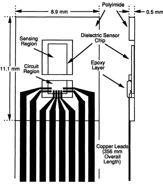
The 8.9 by 11.1 by .5 mm rectangular integrated dielectric circuit chip manufactured by Micromet Industries and typically used for cure monitoring is shown in Figure 3.1. It was encased by a polyimide coating to protect the electronics from the graphite fibers. This circuit chip was used in previous studies to determine the feasibility of implanting sensitive electronic devices in graphite/epoxy [16]. The circuit chip had lead wires .13 mm thick equal to the width of the chip that extend halfway along the tensile coupon.
A G1195 piezoceramic material manufactured by Piezo Systems was implanted as an example of a strain actuator. This piezoceramic
a U Polyimide .
'-d- 0.5 mm
Figure 3.1 Enlarged View of Micromet Integrated Dielectric Circuit Chip and Lead Attachment
11.1
material had a high modulus and curie temperature. The high modulus allows the PZA to carry loads within the graphite/epoxy and the high curie temperature protects the material during the cure cycle. Piezoceramic material will cause a bending moment when two piezoelectrics are bonded or embedded at opposite but equal distances from the neutral axis of the composite material and a voltage is applied across the PZA. The properties of the piezoceramic are shown in Table 3.2. Y11 is the modulus in the length or width direction. Y33 is the modulus in the .25 mm thickness direction. Because these experiments were not focused on the operation of the embedded sensors, actuators, or circuitry, only a single PZA with two lead wires was embedded instead of the pair normally required for actuation.
The PZA material was purchased in 64 by 38 by .25 mm sheets. Each sheet was cut with a sharp razor and straight edge into four 16 by 38 by .25 mm pieces. The lead wires were easily cut with a razor from the leads of integrated dielectric circuit chips and consisted of two of the
eight copper wires. 1.5 mm of polyimide coating on one end of the lead wires had to be scraped off with a razor to allow soldering of the wires to the PZA. The lead wires were placed on opposite edges of the PZA, one on the top and one on the lower surface, halfway along its length as shown in Figure 3.2. M-FLUX AR manufactured by Measurements Group helps the solder adhere to different surfaces and was put on the PZA where the end of the lead would be attached and also on the bare copper wires on the leads. Both the PZA and the lead wires were painted with solder which minimized the size of the finished solder joint. The lead wire tips were straightened after the solder was painted on. Methanol was used to clean up the M-FLUX around the painted solder
Table 3.2 Material Properties of Piezoceramic Material
Moduli:
Density:
Curie Temperature: Tensile Static Strength: Tensile Dynamic Strength: Thermal Expansion Coefficient: Compressive Strength: Y33 = 4.9 x 10¹⁰ N/m2 Y11 = 6.3 x 10¹⁰ N/m2 7600 kg/m3 3600C 6.3 x 10⁷ N/m2 2.1 x 10⁷ N/m2 5 x 10⁻⁶ m/m C 5.2 x 10⁸ N/m2
Y33 = Modulus through Thickness
Kapton
I I
38.1
I
Figure 3.2 Schematic of Piezoceramic Implant with Lead Wires Attached
on both the PZA and leads. The leads were then soldered to the PZA such that the lead wires were aligned with the sides of the implant. The PZA and the portion of the leads along the PZA were encased in .075 mm thick Kapton film with pressure sensitive acrylic epoxy manufactured by 3M which electrically insulated the PZA from the graphite fibers. The acrylic adhesive had a lamination temperature of 135-1501C and a maximum operating temperature of 1050C for short-term exposures. Piezoceramic material is extremely brittle and caution had to be exercised to avoid cracking it during this process.
The teflon implants were manufactured by Altec Plastics. A 305 by 305 by 0.5 mm thick teflon sheet was cut into 9 by 11 mm rectangles to simulate the size of the circuit chip. A 305 by 305 by 0.25 mm thick teflon sheet was cut into 16 by 38 mm rectangles to simulate the size of the PZA. The thickness of the teflon chip was equivalent to the actual chip implant thickness. The thickness of the teflon PZA was equal to the thickness of the PZA material but was only one half the thickness of the combined PZA, film coating and lead wires. These teflon pieces were used to investigate how the material properties of the implant affected the tensile strength of the coupons and also to compare how well the actual implants versus teflon bonded to the graphite/epoxy. The material properties of teflon are shown in Table 3.3. Because of the difficulty in attaching anything to teflon, there were no lead wires attached to the teflon pieces. The teflon, chip, PZA and optical fibers were placed directly into the composite with no additional bonding material. Figure 3.3 shows a comparison of the chip, PZA and teflon implants' relative sizes and shapes.
Material Properties of Teflon
Note: Properties as quoted by Altec Plastics Table 3.3
Tensile Strength 6.9 GPa - 27.6 GPa
Melting Point 326.67 OC
Specific Gravity 2.16
Coefficient of Linear Thermal 13.33 in/in OC x 10-6 Expansion (CTE)
- 50 mm
111
mm,
38 mm II Ii II"mm
-I
I: U' .40 mm .66 mm PZA 50 mm --. aph ipox min; 8.9 mmL5
mm
Graphite/ Epoxy Laminate Laminate Thickness.5 mm
Laminate Thickness Teflon ChipComparison of Implant Sizes
.25 mm Teflon PZA
I
l .13 mm .5 mm Circuit Chip i ,.= `11ý Figure 3.3 I I I I IThe matrix showing all the combinations of implants and layups that were manufactured is shown in Table 3.4. A total of 5 tensile coupons were manufactured for each variation of layup and implant. A set of "virgin" specimens without implants was made and tested to validate theoretical mechanical properties of the laminate and to have an experimental comparison to the specimens with implants. A common type of layup used in industry is the quasi-isotropic laminate layup 2. This was the primary layup used to study the effect of laying over the implant vs. cutting out plies and to make a comparison between the effects of using teflon versus the chip and PZA implants. The tensile specimen configuration is shown in Figure 3.4.
3.2 Manufacturing Procedure of Tensile
Coupons
All experimental work was performed in the Technology Laboratory for Advanced Composites. Manufacturing, instrumenting and testing was performed using procedures described in the TELAC Manufacturing Class Notes [19]. Special procedures described in the following sections 3.2.1-3.2.4 were developed for inserting the implants into the laminates.
The individual plies were cut from a 305 mm wide roll of unidirectional AS4/3501-6 prepreg manufactured by Hercules. The tensile coupons were manufactured from a 305 by 356 mm plate. Cutting 0 degree plies was straightforward. The cutting of ±45 degree and 90 degree plies from unidirectional tape was slightly more complicated and is illustrated in Figure 3.5. The plies were laid up by
Table 3.4 Number of Coupons Manufactured Implant Layup 1 2 3 4 [0/(±45)2/90/(±45)2]s [0/+45/901]2s [45/0/-45/0/90/-45/0/-45/0/451s [454s Virgin 5 5 5 5 Specimens Circuit Chip 5 5 5 5 Implants Placed in Cut Laminate PZA Implants 5 5 5 5 Placed in Cut Laminate Optical Fibers 5 5 5 5 Placed Directly in Laminate Teflon Circuit 5 Chip Placed in Cut Laminate Teflon PZA 5 Placed in Cut Laminate Circuit Chip_ _ 5 Placed Directly in Laminate Optical Fibers _-_ 5 Placed in Cut Laminate
50 mmi
00
900 Tensile Specimen 75 mm 200 mm 75 mm 4- -Graphite Epo . Glass/Epoxy Loading Tab FM-1 23 Film Adhesive T Figure 3.4 IPieces to be Attached to 305 mm by 305 mm Piece 00 Laminate Direction Creation of 900 Layer 25mm 248 mm Creation of 450 Layer 00 Laminate Direction
-f
356 mm 305 mmCreation of 450 and 900 Ply From Unidirectional Tape
1
305 mm356 mm
-I
Figure 3.5 .305 mm 305 mmhand against a 90 degree metal dam used to maintain consistent angular orientation of the plies and to keep two "neat" sides of the laminate that were used to align the laminate in the milling machine later.
The piezoceramic, chip and teflon implants were all placed in cut-out areas in the center of the laminate. The depth of the cutcut-out was based on the assumption of a nominal .135 mm graphite/epoxy ply thickness. When the laminate was complete, the corner that lay in the metal frame was marked and the plate was trimmed to 305 by 356 mm. The edge where the leads extended was originally left untrimmed in an effort to help locate the position of the implants after the cure; however, the implants were successfully located using X-rays and all of the edges were later trimmed prior to the cure. When the leads were allowed to hang out of the laminate, excessive epoxy leaked out of the cure packaging. Sheets of 406 by 305 mm peel ply were placed on both sides of the laminate after they were assembled. The peel ply created a slightly roughened surface texture after the cure. The rough texture helped create a stronger bond between the graphite/epoxy and loading tabs and strain gages. The peel ply extended 50 mm past one end of the laminate to aid removal after the cure.
All laminates were placed in vacuum bags sealed with vacuum tape overnight at room temperature before being cured the following day.
3.2.1
Implanting Circuit Chips
The circuit chip thickness of .5 mm was equivalent to four cut plies of .135 mm thick graphite/epoxy and the lead wire thickness of .13 mm was equivalent to one cut ply. The lead wire ply was an extension of the fourth cut ply. A cardboard template shown in Figure 3.6 was used to cut five rectangular holes 10 by 12 mm out of a three ply sublaminate. There was a separate template for the fourth layer with the leads which is also shown in Figure 3.6. The implants were spaced 58.5 mm apart to allow an extra 8.5 mm between coupons. This machining allowance assured each 50 mm wide coupon had a centered implant.
The method used for implanting the chips was identical for all four layups. The only difference was the ply orientations in the sublaminates. The sublaminate approach to inserting the implants is shown in Figure 3.7. In order to implant the chip into layup 1, the bottom sublaminate consisting of [0/45/-45/45/-45/90/45/-45] plies was laid down and then a sublaminate consisting of [45/-45/-45] plies was put together. The three ply sublaminate had five rectangular 10 by 12 mm holes cut into it using the template shown in Figure 3.7. This sublaminate was then placed onto the existing lay-up. The last [45] ply used for the implant leads was cut using the lead wire template and then carefully placed onto the main lay-up so as to align the lead holes with the main chip cutout. Five circuit chips were then placed in the holes with the lead wires aligned with the cut-out areas in the plies. A 3 by 5 mm piece of 0.28 mm thick #34 glass filter paper manufactured by Schleicher & Schuell was put on top of the silicon chip to insulate the


![Figure 4.3 Stress-Strain Curves for Virgin Coupon 3V-B with a Layup 3, [45/0/-45/0/90/-45/0/-45/0/45]s, Configuration Tested to Failure1000800o4002000](https://thumb-eu.123doks.com/thumbv2/123doknet/14757241.583186/88.918.116.752.253.778/figure-stress-strain-curves-virgin-coupon-configuration-failure.webp)
![Figure 4.8 Stress-Strain Curves for Coupon 20F-E with Optical Fiber Placed Directly in Laminate with a Layup 2, [0/±45/90]2s, Configuration Tested to Failure](https://thumb-eu.123doks.com/thumbv2/123doknet/14757241.583186/94.918.116.755.255.773/figure-stress-strain-optical-directly-laminate-configuration-failure.webp)
![Figure 4.9 Stress-Strain Curves for Failure with Chip Placed in [0/±45/90]2s, Configuration](https://thumb-eu.123doks.com/thumbv2/123doknet/14757241.583186/95.918.114.755.258.777/figure-stress-strain-curves-failure-chip-placed-configuration.webp)

![Figure 4.11 Stress-Strain Curves for Coupon 2TC-C with a Layup 2, [0/± 4 5 / 9 0 ]2s, Configuration Tested to 90% of its Ultimate Stress7006004003002001000 0.012](https://thumb-eu.123doks.com/thumbv2/123doknet/14757241.583186/97.918.119.759.254.773/figure-stress-strain-curves-coupon-configuration-tested-ultimate.webp)
![Figure 4.12 Stress-Strain Curves for Coupon 2TP-E with a Layup 2, [0/± 4 5 / 9 01]2s, Configuration Tested to 95% of its Ultimate Stress7006005004003002001000I](https://thumb-eu.123doks.com/thumbv2/123doknet/14757241.583186/98.918.125.762.260.776/figure-stress-strain-curves-coupon-configuration-tested-ultimate.webp)