The Effect of Proton Bombardment on Semiconductor
Saturable Absorber Structures
by
Juliet Tara Gopinath
B.S., Electrical Engineering University of Minnesota, 1998
Submitted to the Department of Electrical Engineering and Computer Science in Partial Fulfillment of the Requirements for the Degree of
Master of Science
at the
Massachusetts Institute of Technology
September 2000
@ Massachusetts Institute of Technology, 2000. All rights reserved.
Signature of A uthor...
Department of Electrical Engineering and Computer Science September 1, 2000
Certified by...ich...
Erich Ippen
Elihu Thompson Professor of Electrical Engineering -~~~ 2Thesm Supervisor
Certified by... . . . . ... .. ...
Arthur C. Smith Chairman, Department Committee on Graduate Students
MASSACHUSETTS INSTITUTE OF TECHNOLOGY
OCT 2 3 2000
BARKER
The Effect of Proton Bombardment on
Semiconductor Saturable Absorbers
by
Juliet Tara Gopinath
Submitted to the Department of Electrical Engineering and Computer Science on September 1, 2000 in partial fulfillment of the requirements for the
Degree of Master of Science
Abstract
Carrier lifetime reduction resulting from proton bombardment of InGaAs/InP-based semiconduc-tor saturable absorbers was studied experimentally, using a standard degenerate, cross-polarized pump-probe technique. Proton bombardment reduced carrier lifetimes by as much as a factor of 40 at low optical excitation densities. For high fluences, significant induced absorption was observed. The recovery of this excited state absorption did not show as significant a dependence on the level of proton bombardment. It is possible that the cause of this induced absorption - car-riers outside the InGaAs quantum wells, highly excited carcar-riers, or those trapped in satellite val-leys - is not sensitive to the effects of bombardment. Also, the bombardment-created defects may saturate at such high fluences. The detrimental side-effects of proton bombardment -reduced modulation depth and increased non-saturable loss -have been shown to be mitigated with a short post-growth anneal. Finally, modelocking was demonstrated with the proton-bombarded samples in an erbium fiber laser.
Thesis Supervisor: Erich P. Ippen
Title: Elihu Thompson Professor of Electrical Engineering
Acknowledgements
I am grateful to Professor Ippen for his guidance and supervision. Without his insights on
experi-mental techniques and intuition about the physics studied in this experiment, this thesis would not have been possible. I enjoy working in his group, the research, and his warm personality and good sense of humor. I thank Professor Haus for also stimulating me and keeping me on my toes.
I am indebted to Erik Thoen for teaching me how to perform the measurements in this thesis and helping me through many of the experimental bugs. He was (and still is) never too busy to spare a minute to discuss data, despite an extremely hectic schedule. He seems to have a supply of infi-nite patience and was always willing to bail me out with my endless problems with the OPO (Optical Parametric Oscillator) even from home! I thank Elisabeth Marley Koontz for growing the structures studied, and for her help and insights with the experiments, although she still calls me a "kid"! Also, I thank both Erik and Elisabeth for their friendship. Without them, this thesis would not have been possible!
Dan Ripin was often able to give me good advice and gave much needed encouragement. He was always willing to explain difficult concepts with clarity and to lend a hand in lab, and has also been quite a walking encyclopedia of Boston-area restaurants! Matt Grein has encouraged me along the way, and taught me all I know about fiber lasers to date. He has been generous with his time and explanations. Leaf Jiang has also been helpful -whether it be with computer problems or lab equipment. I thank my officemates, Pei-Lin Hsiung (I owe her many a dinner), Rohit Prasankumar, and John Fini for all their camaraderie (and wondering where I was that week I took off for vacation without telling them)! I thank the rest of the group for their friendliness and help: Peter Rakich, Milos Popovic, Pat Chou, Charles Yu, Christine Manolatou, Jalal Khan, Mike Watts, J. P. Laine, Dr. Yijang Chen, Dr. Franz Kartner, and the Fujimoto contingent of Seong-Ho Cho, Tony Ko, Costas Pitris, Andrew Kowalevicz, Kathleen Saunders, Ravi Ghanta, Dr. Ingmar Hartl, Dr. Christian Chudoba, Dr. Xing-De Li, and Dr Kaoru Minoshima. From Professor Leslie Kolodziej ski's group, Dr. Gale Petrich has also been helpful (and also one of few here who
stands the meaning of cold weather). I'd also like to thank the three group secretaries Cindy Kopf, Mary Aldridge, and Donna Gale for all their help and interesting gossip.
Dr. Markus Joschko and Dr. Patrick Langlois did much pump-probe that has helped us to under-stand these structures better. I thank Dr. Joe Donelly for many insightful discussions about proton bombardment and annealing. Bob Bailey at Lincoln Labs also provided help and resources. I thank Elisabeth L. Shaw for help with the CMSE facilities and Peter O'Brien at Lincoln Labs for coating deposition.
I am grateful for the support of a National Science Foundation fellowship.
I thank Professor James Leger, Professor Mostafa Kaveh, Professor C. C. Huang (University of
Minnesota) and Professor Gadi Eisensten (Technion, Israel Institute of Technology) for their guidance, advice, and encouragement as well as the research opportunities they provided.
I thank Professor Marcus Thompson, my viola teacher here at MIT, for wonderful lessons and
musical opportunities that have preserved my sanity while working on this thesis. Thanks to my Grieg string quartet for also providing stress relief and putting up with this project! I am grateful to all my friends for their support and for putting up with all the complaints that went along with this thesis.
I thank my parents and my little sister, Charlotte, for their support and love. Without their inspira-tion and help, I don't think that I'd be here at MIT. I am very excited to be finishing this thesis. I'm still wondering whether it is a dream. Thank you all for making it real!
Table of Contents
Acknowledgements
Chapter 1 Introduction
Chapter
2
Chapter 3
Chapter 4
Semiconductor Saturable Absorbers
11
2.1 Review of Modelocking Techniques...11
2.2 Saturable Absorber Theory... 16
2.3 Types of Saturable Absorbers... 24
2.4 Absorber Lifetime Reduction Techniques...25
2.5 Growth of Semiconductor Saturable Absorbers...28
2.6 Optical Characterization of Saturable Absorbers...34
Experimental Design
36
3.1 Pum p-Probe Theory... 363.2 L aser Sources... 37
3.3 Experim ental Setup... 40
Experimental Results
43
4.1 Pump-Probe of Non-Proton-Bombarded Absorbers...43The Effect of Proton Bombardment on Semiconductor Saturable Absorber Structures
5
9
Pump-Probe of Proton-Bombarded Absorbers...58
Pump-Probe of Proton-Bombarded InP Structures...73
Laser Results from Proton-Bombarded Absorbers...77
Chapter
5
Conclusions and Future Work
80
5.1 C onclusions... 80 5.2 Future W ork... 81
References
83
The Effect of Proton Bombardment on Semiconductor Saturable Absorber Structures 4.2
4.3
4.4
Chapter 1: Introduction
Saturable absorbers have been used for passive modelocking for many years. With the recent explosion in telecommunications, their use for the generation of short pulses at 1500 nm is of par-ticular interest. Semiconductor saturable absorbers often exhibit a bitemporal response, consist-ing of fast and slow components. The fast time constant is on the order of 100 fs to several picoseconds, and results from intraband dynamics. The slow time constant, due to recombination, is on the order of picoseconds to several nanoseconds, depending on the materials system and growth parameters. For a saturable absorber to be useful at high repetition rates and for pico- and femtosecond pulse generation, it is important to reduce the long recovery time constant.
Lifetime reduction in a semiconductor can be accomplished by the introduction of defect states. Much research has been done on the use of low-temperature growth and ion bombardment for this purpose. The effect of proton bombardment on semiconductor saturable absorbers at 1500 nm is the subject of this thesis. To the best of my knowledge, there have not been previous studies of the effects of proton bombardment on this particular type of saturable absorber. In addition, experi-ments have not been conducted at 1.5 jm, the telecommunications wavelength, or extensively at high fluence, important for the operating conditions of lasers.
Time resolved spectroscopy is ideal for studies of absorber recovery times. I performed measure-ments, using a cross-polarized collinear degenerate time-resolved pump-probe technique. With
150 fs pulses from an Optical Parametric Oscillator (OPO), tunable from 1400 to 1600 nm, I
achieved a time resolution of 300 fs and minimum detectable signal levels of 10-3. Proton-bom-barded absorbers that were characterized were then tested in a 17 MHz erbium fiber laser.
In Chapter 2, the motivation and theory of modelocking with saturable absorbers is discussed. A brief review of modelocking techniques is presented, and then a discussion of saturable absorber theory follows. Previous work on saturable absorber lifetime reduction is presented. Finally, a description of the devices investigated and the fabrication process is presented. Chapter 3 con-tains a description of the experiment design and theory. The characteristics and limitations of the
laser system used for the pump-probe measurements are discussed. Details of the experimental setup are described. In Chapter 4, experimental results are presented. At low fluences (fluences less than the absorber saturation fluence), proton bombardment can reduce lifetimes up to a factor of 40. However, at high fluences (fluences greater than the absorber saturation fluence), signifi-cant induced absorption is observed. The recovery of this induced absorption does not show a sig-nificant dependence on the level of proton bombardment. It is possible that the cause of this induced absorption -carriers outside the InGaAs quantum wells, highly excited carriers, or those trapped in satellite valleys -is not sensitive to the effects of bombardment. Also, the bombard-ment-created defects may saturate at such high fluences. The detrimental side-effects of proton bombardment -reduced modulation depth and increased non-saturable loss -are shown to be mit-igated with a short post-growth anneal. Finally, the results of tests in a linear erbium fiber laser are presented. All proton-bombarded absorbers studied modelocked the laser, and for two of them, self-starting modelocking was observed. In Chapter 5, conclusions and future work are dis-cussed.
Chapter 2: Semiconductor Saturable
Absorbers
This chapter contains a brief review of modelocking techniques, to motivate interest in developing more effective semiconductor saturable absorbers. The parameters that can be adjusted in satura-ble absorber design are discussed; specifically, the importance of absorber lifetime reduction is addressed. Two different techniques for lifetime reduction are presented: ion bombardment and low-temperature epitaxial growth. The fabrication process for the absorbers studied in this thesis is described, along with a short description of the optical characterization necessary for accurate growths.
2.1 Review of Modelocking Techniques
With the current revolution in Internet and communications, the demand for bandwidth doubles every 100 days, creating a demand for higher repetition rate, shorter pulse sources. Ultrashort pulses also have important applications in spectroscopy, high resolution imaging technology, and
surgery. In the past thirty years, the generation of short pulses has been revolutionized: from
pulses of 10-11s to pulses of femtosecond length, a decrease of four orders of magnitude. The first
sub-picosecond pulses where produced in 1974 [23], with a dye laser. Semiconductor diode lasers and color center lasers were modelocked in a similar fashion, using slow saturable absorber modelocking. However, advances in ultrashort pulse generation in solid-state lasers (below
second pulses) only picked up pace in the 1980's, with the use of fast, reactive nonlinearities for modelocking. Currently, 5 fs pulses, about two optical cycles long, have been produced from a Titanium:sapphire (Ti:sapphire) laser [48] [56], using Kerr lens modelocking (KLM).
0-11
101
1 01
10 14
Nd:glass Nd:YAG Nd:YLF
Dye S-P Dye Diode CW Dye Color Center Cr:YAG Cr:LiS(C)AF CPM Er:fiber Cr:forsterite Nd:fiber Compression Ti:sapphire I I I I I I I 1 1965 1970 1975 1980 1985 1990 1995
FIGURE 2.1 History of ultrashort pulse generation. The achieved pulse width versus year for several different types of lasers systems. Figure from [23].
In a modelocked laser, the phases of a group of longitudinal modes (frequencies) are "locked" together. To produce modelocked operation, a variety of techniques, both active and passive, can be employed to favor a pulsed state over continuous-wave operation. All techniques involve the
introduction of an intensity-dependent loss into the system.
Amplitude modulation, developed thirty-five years ago, is one method of short pulse generation. An amplitude modulator can be placed in a laser cavity, providing amplitude filtering at the cavity round-trip frequency. A pulse arriving at maximum transmission experiences minimum loss; thus shorter pulses see less loss than longer ones. However, shorter pulses are shortened progressively
less and less by the modulator [23]. Therefore, active modelocking is not suitable for the produc-tion of ultrashort pulses.
Shorter pulses can be generated with passive modelocking techniques in which the laser self-mod-ulates itself. Most of these passive techniques fall under the general heading of saturable
absorber modelocking. These methods have been demonstrated in both solid-state and fiber lasers, stimulated by the advent of broadband gain media in the last decade.
Pulses can be generated with so-called "real" saturable absorbers, absorbers that rely on material excitation to produce intensity-dependent loss. As intensity increases, the transmission of these
"real" absorbers increases, thus favoring shorter pulses with higher peak intensities. Semiconduc-tor saturable absorbers, the subject of this thesis, can be used in several different ways to mode-lock lasers. In so-called "slow" saturable absorber modemode-locking, the leading edge of the pulse is
shaped by the saturable absorber response. However, the saturable absorber recovery time is not fast enough to shape the trailing edge of the pulse. Instead, the trailing edge of the pulse is shaped
by the gain recovery of the laser medium itself. With this technique, pulses much shorter than the
recovery time of the absorber can be produced [23].
Pulses can also be generated with "fast" saturable absorber modelocking. With this method, the absorber itself shapes both the leading and the trailing edges of the pulse. Thus, one is limited in "fast" saturable absorber modelocking by the recovery time of the absorber. Since real saturable absorbers rely on material excitation to produce their intensity-dependent loss, the response time is dominated by the recovery of the medium. This usually occurs on a picosecond or nanosecond scale, depending on the materials system and fabrication techniques. Thus, semiconductor satu-rable absorbers are often used in "slow" satusatu-rable absorber modelocking.
Fast saturable absorber modelocking is often implemented with so-called "artificial" absorbers. Artificial saturable absorbers rely on the index nonlinearities of transparent media, often the gain medium itself. In artificial saturable absorbers, changes in the refractive index with intensity are converted to amplitude modulation. Because saturable absorption action is produced through non-resonant optical nonlinearities, it is fast. Currently, the shortest pulses out of a solid-state
laser to date, 5 fs from a Ti:sapphire, are produced by Kerr lens modelocking, an artificial absorber technique [48] [56].
With the Kerr nonlinearity (the nonlinear change of index of refraction with intensity), loss modu-lation can be introduced into the system by adding an aperture that allows more intense pulses a greater transmission. An actual aperture can be introduced into the system (hard aperture KLM) or the gain medium can play the role of an aperture when it varies spatially (soft aperture KLM). However, in Kerr lens modelocking, the laser cavity is typically operated near the edge of the sta-bility regime, thus requiring systems to be critically aligned within several hundred microns.
Polarization additive-pulse modelocking (APM), also uses the Kerr nonlinearity as an artificial absorber. It is often used in fiber lasers, because the nonlinearity is weak, but the interaction length is long. The cavity contains a Kerr medium, so that the pulse in this cavity experiences self-phase modulation, causing an dependent phase shift, which can result in intensity-dependent polarization rotation. With the addition of polarizers, this can be converted into an intensity-dependent loss, or self-amplitude modulation (SAM) [23]. This technique has mainly been applied to fiber lasers, with pulses as short as 77 fs generated from Er doped systems [18]. However, it is difficult to build high-repetition rate APM sources because long interaction lengths are needed to produce the polarization rotation.
One drawback of artificial saturable absorbers is that they are weak, a direct consequence of reli-ance on a non-resonant nonlinearity of the gain media (incidentally, the fact that gives them speed too). Thus, self-starting is a problem of artificial absorber systems, as extremely high peak inten-sities are required for the nonlinearity to take effect. Real semiconductor absorbers can be used to self-start artificial absorber systems, as they have much lower saturation fluences than artificial absorbers. They also relax the constraint on critical cavity alignment required for KLM [29] [56]. Self-starting 6.5 fs pulses from a Kerr lens modelocked Ti:sapphire laser have been achieved with an intracavity saturable absorber [28].
Pulses can also be generated by soliton modelocking, in which a pulse is shaped by the balance between dispersion (causing temporal broadening) and self-phase modulation (causing spectral
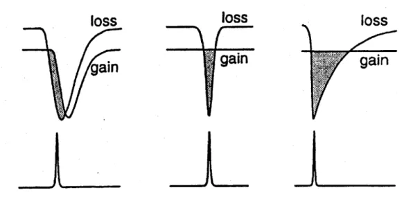
broadening). In both slow and fast saturable absorber modelocking, a relatively short net-gain window exists. However, in soliton modelocking, it has been shown that the net gain window can remain open for up to ten times longer than the actual pulse [32], leaving room for instabilities to grow. The soliton can shed to the continuum, causing instabilities and eventual pulse breakup. The addition of a saturable absorbers can filter out this continuum, increasing overall system sta-bility [31].
loss
loss
loss
gi gain
gain
FIGURE 2.2 The three passively modelocking models. From left to right: (a) passive modelocking with a slow saturable absorber and dynamic gain saturation (b) fast saturable absorber modelocking and (c) soliton
modelocking. Figure from [32].
In summary, there are many techniques, active and passive, that can be used to generate short pulses from lasers. Passive methods are capable of producing shorter pulse widths than active techniques, since active techniques are inherently limited by the speed of electronics. Semicon-ductor saturable absorbers (so-called "real" absorbers) are one way to produce short pulses pas-sively. Although the shortest pulses to date have been produced with Kerr lens modelocking, this technique is difficult to start. Semiconductor saturable absorbers do not suffer from these starting problems, and in addition, can be used to stabilize techniques such as Kerr lens modelocking and soliton modelocking. They are important for optical applications such as all-optical switching. In a world in which devices are shrinking and increasing in speed, saturable absorbers are an important component.
2.2
Saturable Absorber Theory
The history of saturable absorbers begins about the time the solid-state laser was invented. In
1965, Mocker and Collins used dye and color filter saturable absorbers to modelock a ruby laser
[47]. Twenty years ago, semiconductor nonlinearities were used to modelock a semiconductor laser with a reduced recovery time, induced by aging [22]. Fifteen years ago, a multiple quantum well structure was used to modelock a semiconductor diode laser [52]. The first solid state laser modelocked with an intracavity saturable absorber was a color-center laser in 1989, producing
275 fs pulses [25]. Since then, saturable absorbers have been used to passively modelock many
solid-state lasers, including Nd:YLF, Nd:YAG, Nd:LSB, Nd: YVO4, Cr4+:YAG and Cr:fosterite
[29]. They have also been used to modelock fiber lasers, achieving repetition rates three times
higher than those achieved by APM [36]. The first fiber laser modelocked with a transmissive sat-urable absorber was reported in 1991 [64]. Later, a semiconductor saturable absorber deposited on a distributed Bragg reflector was used to generate sub-picosecond pulses from a linear fiber cavity [43] [44].
With the advent of bandgap engineering and innovations in materials processing, today, there is much freedom in absorber design, and devices can be tailored for specific applications. Semicon-ductor saturable absorbers provide a compact bulk nonlinearity that does not require critical align-ment, and is easily integrable into compact optical systems. As pulses become progressively shorter, there is also growing interest in developing broad-band saturable absorbers.
Semiconductor saturable absorbers modelock or assist in modelocking lasers, because, like every other modelocking technique, they introduce an intensity-dependent loss. States with higher peak intensity (i.e. shorter pulses) are favored. Semiconductor saturable absorber mirrors are basically nonlinear mirrors whose operation relies on carrier excitation. For absorbers used in a reflective geometry, the basic design is a layered Bragg stack (DBR), on top of which is absorbing material,
either in the form of quantum wells or bulk sections. This absorbing material produces the non-linear reflectivity response of the mirror. Light at a designed wavelength excites carriers from the valence to the conduction band, and is absorbed. As the incident light becomes increasingly intense, more and more carriers are excited. Eventually, all of the available states in the conduc-tion band become full. At this point, the absorber is "bleached", and light is no longer absorbed and instead, fully reflected from the DBR.
The basic design parameters of a general saturable absorber are: saturation intensity, Isat;
satura-tion fluence, Fsat; modulasatura-tion depth or saturable loss; and recovery time. These parameters
deter-mine the startup modelocking conditions, the resilience of the system against Q-switching and other instabilities, and the shortest pulse width achievable.
A saturable absorber has both nonsaturable and saturable loss. Loss that has no power
depen-dence is nonsaturable. In the ideal absorber, the non-saturable loss would be zero. Low-gain lasers, in particular, cannot tolerate much non-saturable loss. The more non-saturable loss in a system, the closer to threshold it becomes, which increases susceptibility to instabilities. In con-trast to non-saturable loss, saturable loss is intensity-dependent loss. The modulation depth of an absorber is the total amount of saturable loss of the absorber: the amount of loss that can be satu-rated by a high-intensity pulse. The modulation depth, AR ~ 2col, of an absorber is related to the
pulse width produced as follows [29]:
n
T a (1)
TP
where n varies, depending on the type of modelocking used [20] [21] [31]. Thus, shorter pulses can be achieved with higher saturable losses.
The saturation intensity of the absorber is important for initial pulse creation in laser systems. Noise fluctuations in the laser system lead to pulse formation. In this regime, the continuous-wave (cw) intensity of the light incident on the absorber determines the saturation behavior of the absorber. The absorber should be barely saturated (if it was saturated, pulses would not be favored) and act as a fast absorber, with a recovery time much faster than the noise fluctuations. (When the laser modelocks, and the pulses become short relative to the absorber recovery time, the absorber acts as a "slow" saturable absorber.) In the cw regime, the saturation intensity is given as [32]:
Isat = (2)
GATA
where ho is the photon energy, TA the absorption cross-section and TA, the absorber recovery time. The absorption cross-section, defined to be the absorption probability per incident photon flux, or the absorption coefficient per absorption center, is a material parameter [3]. From the
absorption cross-section, we can define an absorption coefficient of the material to be:
a = NDcA (3)
where ND is the density of the absorber atoms, or density of states (semiconductors). In the cw
state, the absorption coefficient saturates as
(X = Ls + 0 (4)
1+
-Isat
where a1ns is the nonsaturable loss of the absorber, ao is the saturable loss of the absorber, and Isat is the cw saturation intensity of the absorber [33].
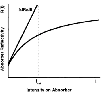
IdR/dII
0
I-a
Intensity on Absorber
FIGURE 2.3 Nonlinear reflectivity of a saturable absorber mirror due to absorption bleaching from cw intensity. Reflectivity is denoted by R, and intensity by 1.
The modelocking buildup time will be proportional to the slope of the increase in reflectivity vs.
the change in intensity at I ~ Icw~0, as shown in Figure 2.3. Under certain approximations [32],
we can write:
Tbuildup(X dR I I ;w, (5)
where dR/dI represents the change in absorber reflectivity vs. cavity intensity. The larger the slope of the saturable absorption, the smaller the intensity fluctuation required to produce a reflec-tivity change in the absorber itself. This means that as saturation intensity decreases, modelock-ing time decreases also.
However, if the laser is in a modelocked, or pulsed regime, the intensity is a function of time. Once the pulses become significantly shorter than the absorber recovery time, the absorber
becomes a "slow" saturable absorber, assisting to shape one edge of the pulse. Until this condi-tion is true, equacondi-tions (2) -(5) hold. When the absorber becomes a "slow" absorber, it is the
satu-ration fluence rather than the satusatu-ration intensity that is important. The satusatu-ration fluence is written as [4]:
hv
Fsat = - (6)
'YA
The fluence incident on the absorber, F, is given as:
F(t) = I(t)dt (7)
The absorption for a slow saturable absorber, is then given as [33]:
X = ns + F (8)
1+
-Fsat
From the previous discussion, it is clear that the saturation intensity and fluence of an absorber are important for the startup of modelocking. These parameters can also help prevent the growth of instabilities. However, there is a fine balance between the shortest possible mode-locking buildup time, and prevention of instabilities. If the saturation intensity becomes too small, Q-switching takes over. Because the saturation intensity is inversely proportional to the absorber recovery time, shorter lifetimes increase the saturation intensity and system resilience to Q-switching.
Q-switching results in the non-equilibrium buildup of a very intense pulse, that ends when the gain is depleted. The process can repeat itself when the gain recovers. Q-switching mechanisms can be produced via a shutter that blocks an end mirror cyclically or an intensity-dependent loss
with a large saturation energy [35]. A Q-switched envelope can modulate a modelocked pulse train; this is called Q-switched modelocking. The pulses in this state are also quite intense, and can damage saturable absorbers. The state is quite common in startup conditions of saturable absorber modelocked lasers [19]. Sometimes, a small disturbance of the laser cavity can drive a
cw-modelocked laser into a Q-switched modelocked state. This state is undesirable for high repe-tition rate applications that require constant pulse energy.
"single" mode multi mode cw - running cw - Q - switching
o
0time
time
self-starting mode locking
Q - switched mode locking cw - mode locking
0m
time
time
FIGURE 2.4 Different regimes of laser operation with an intracavity saturable absorber. Figure from [32].
To prevent cw Q-switching, the condition following must be satisfied [30] (fast saturable absorber):
I< r
dI l (9)
where r represents the number of times above threshold that the laser is pumped, TR is the cavity
round trip time, and t2 is the upper state lifetime of the laser. Thus, factors in the suppression of
Q-switching include: high absorber saturation intensity (i.e. a small slope, dR/dI), laser operation many times above threshold (large r), low repetition rates (large cavity round-trip times), and small upper state lifetimes, t2 [32]. The right side of the equation is shows the saturation of the gain in the cavity per round trip. The left-hand side describes the loss reduction per round trip due to the bleaching of the saturable absorber. If the gain cannot respond fast enough to the loss
reductions induced by the absorber, intensity in the cavity is no longer constant, and increases with increasing bleaching of the absorber, leading to Q-switching in a stable or unstable form. If the recovery time of the absorber is greater than or equal to the cavity round-trip time, pure cw
Q-switching is favored over modelocked operation [32]. Thus, as the repetition rate of a system increases, the tendency to Q-switch becomes stronger, unless absorber recovery time decreases also.
If an absorber is employed whose recovery time is much less than the cavity round trip time, then
usually equations (5) and (9) are satisfied, allowing short pulse formation. However, in this case, there is an additional stability requirement against Q-switched modelocking. In the following derivations, it is assumed that the pulse width, rp is shorter than the absorber recovery time,
tA-The saturation is now determined by the saturation fluence, Fsat' defined in equation (8). Now, the
loss reduction per round trip is due to the saturation of the absorber by pulses, not from the cw intensity. Obviously, the absorber saturates much further in this limit. The condition for stability against Q-switched modelocking becomes [32]:
dR F< r (10)
d F T 2
This condition can be fulfilled by choosing F, the incident pulse fluence, to be much greater than Fsat- This will also produce maximum modulation depth. Again, however, there is an upper bound to F, given by the onset of multiple pulsing. At a fluence far beyond Fsat' the reflectivity is
no longer strongly affected by the pulse energy. Shorter pulses see a reduced averaged gain also, since eventually, the gain-bandwidth of the laser becomes a limiting factor. Finally, at high enough fluences, given these two factors, a multiple pulse state becomes favored [32].
LL . IdR/dFl .
Multiple Pulsing
F pulse >> F,sa
.0
F
sat Energy Fluence on Absorber F
FIGURE 2.5 Nonlinear reflectivity change of a saturable absorber mirror due to absorption bleaching with short pulses.
The saturation fluence and intensity of the absorber are generally material parameters. The inci-dent spot size is usually adjusted to fulfill the conditions described for stability against Q-switch-ing and multiple pulsQ-switch-ing. In addition, proper placement of the absorbQ-switch-ing layers at the peak or null of the standing wave of the electric field in the absorber can produce variation of the saturation intensity and energy.
The final parameter left to adjust is the absorber recovery time, the subject of this thesis. Because semiconductor absorbers rely on carrier excitation, they exhibit a bitemporal response. The fast response, on the order of several hundred femtoseconds to a few picoseconds, is produced by the thermalization and carrier-carrier scattering, intraband processes. The slow response is due to interband dynamics, the recombination of carriers. Depending on the materials system and growth parameters, this can range from picoseconds to a few nanoseconds. This response time will determine what the dominant modelocking mechanism in the laser system will be: slow
satu-rable absorber modelocking, fast satusatu-rable absorber modelocking, soliton or dispersion-managed
soliton modelocking, or Kerr lens modelocking. Thus, the absorber response time will aid, or fully determine (depending on the modelocking type), the pulse width, the system stability against
Q-switching and other instabilities, and the modelocking self-starting conditions. As intracavity power increases, modelocking build up time decreases. It also decreases with increasing absorber recovery times and decreasing saturation energy.
Pulse widths are partially or solely determined by the response time, depending on the type of modelocking employed. By varying growth conditions and temperatures, or through post-growth ion or proton bombardment, this recovery time can be tailored for the application. As data rates continue to increase, higher repetition rate and shorter pulse systems are becoming important, thus motivating an interest in absorber lifetime reduction.
2.3 Types of Saturable Absorbers
There are several types of saturable absorbers. Absorber structures used in a reflective geometry are placed on a bottom mirror, and a Fabry-Perot cavity is formed between the top surface and the bottom mirror. If the Fabry Perot is operated at antiresonance, an antiresonant saturable absorber is formed; if the Fabry-Perot is operated at resonance, a resonant saturable absorber results.
If the field intensity inside the absorber is less than the incident intensity, the device is an
antires-onant device. In this case, the resulting devices are broad-band and have minimal group velocity dispersion [32]. An uncoated device, with a Fresnel reflection from its top surface, is one special case of an antiresonant device. For low-gain laser systems, such as Cr4+:YAG, the small modula-tion depth associated with such absorbers can be desirable. Another example of an antiresonant structure is an anti-reflection coated device, such that the field intensity inside the absorber is equal the to the incident intensity. In the other limit, the top surface of an absorber could be coated with a high reflector, greater than 95% [32] [58].
At antiresonance, the intensity inside the device is decreased by a factor , compared to the inci-denc intensity [33].
1-Rt (11)
(1 + JRtRbexp(-2i 0d))2
where ao is the absorption coefficient of the absorber, d is the absorber thickness, and Rt and Rb are the top and bottom mirror reflectivities. The saturation fluence decreases by a factor 1/p, and the saturation intensity increases by this same factor.
For higher modulation depths and lower saturation fluences, it is possible to design resonant devices. In these devices, the field inside the structure is enhanced, compared to the incident field. This can be accomplished with a resonant coating on the top of the device. The drawback of res-onant devices is that they are not as broadband; however, for applications requiring high modula-tion depths, they can be useful [59].
The type of coatings added to the top of the saturable absorber structure determine if the absorber is resonant or antiresonant. This adds yet another parameter of freedom to the design of semicon-ductor saturable absorbers. By tailoring the field intensities inside the device, the saturation flu-ence, intensity, and modulation depth can be adjusted.
2.4 Absorber Lifetime Reduction Techniques
Semiconductor saturable absorbers consist of a bitemporal response: an ultrafast response, due to the intraband carrier dynamics, and a slow response, dominated by the interband carrier dynamics.
The slow response time is determined by the carrier recombination time, which in pure materials is on the order of several nanoseconds. This recovery time makes design of ultrafast optical devices difficult. Reduction of this response time can be accomplished by introducing defect states into the material. The lifetime can also be reduced by tightly focusing onto the sample, causing carriers to diffuse out of the interaction region at a speed faster than the device recovery time [53]. However, a small spot size causes the absorber to saturate at low powers.
Efforts to reduce recovery times via defect introduction have a long history. The first semicon-ductor diode laser to be modelocked with semiconsemicon-ductor nonlinearities had a reduced recovery time induced by aging [22]. Shortly afterwards, proton bombardment was used for lifetime reduc-tion [62]. The first solid state laser to be modelocked, in 1989, was modelocked with a proton-bombarded saturable absorber [25]. Defect states can be introduced in material through strain, low-temperature molecular beam-epitaxy (LT-MBE) growth, or through post-growth ion or neu-tron bombardment. These defect states serve as recombination sites, thus decreasing the recovery time of devices. For lifetime reduction, LT-MBE growth and ion bombardment are the two meth-ods. Both techniques have been used in demonstrations of passive modelocking [32] [41]. The techniques both introduce defects, smearing the bandedge by the introduction of near-bandedge states. High defect densities can cause changes in saturation fluence [33]. The saturation inten-sity of the absorbers is affected also, as it depends on absorber recovery time. From the previous section, recall that shorter recovery times can stabilize against Q-switching, but are not helpful for self-starting. Disadvantages of the lifetime reduction techniques include increased non-saturable loss and reduced modulation depth. There is still discussion as to the origin of the increased non-saturable loss: introduction of mid-gap traps is one possible explanation [41]. Carriers may be captured by these trap states, then re-excited, and finally recombine. If the trap states created have transitions that are difficult to saturate, they contribute to the non-saturable loss, and reduced modulation depth. The increased nonsaturable loss and reduced nonlinearity of the devices can be mitigated with a post-process anneal (for both MBE and ion bombardment). In the case of LT-MBE, dopants can also alleviate these detrimental side effects. The sharpness of the bandedge
can be restored with annealing and or the addition of dopants [54]. The physics behind the bene-fits of annealing are not well understood [9]; however, it may allow the defects to find the lowest
energy stable states. Some of the trap states are probably converted into recombination centers
[54], and annealing may remove some of the shallow states, improving stability [51].
The effects of low-temperature (LT) epitaxial growth on the recovery times of semiconductor sat-urable absorbers has been studied extensively. In conventional MBE systems, the substrate is
heated to -500 or -600 0C respectively for GaAs and InP, producing high optical and electrical
quality material [16]. Low-temperature growth causes the material quality to decrease, conse-quently reducing the lifetime. This method has been studied with various materials systems including: GaAs[45] [50], InGaAs/ InAlAs [27] [57], InGaAs/InP [16], and AlAs [37]. All of these materials contain arsenic, and low-temperature growth causes As-rich conditions, inducing excess-As caused defects in the form of precipitates, interstitials, microclusters, and vacancies. In low-temperature GaAs and InGasAs, beryllium doping, as well as annealing, has been shown to mitigate non-saturable losses and decreases in modulation depth resulting from LT growth. It is thought that beryllium doping changes the type of trap created. The traps created with this dopant have a transition that is easier to saturate than that of the traps resulting from non-beryllium doped LT-GaAs or LT-InGaAs growth [17] [27]. Subpicosecond relaxation times have been observed in LT GaAs, LT InAlAs/InP and lifetimes have been reduced to 2.5 ps for LT InGaAs/InP [16].
Ion implantation is a commonly used technique in semiconductor processing. Unlike LT epitaxial growth, it is a relatively simple post-growth step and is a more mature processing procedure [14]. In semiconductor saturable absorbers, a variety of ions have been used for lifetime reduction: pro-tons [51], arsenic [42], oxygen [42], gold [5], helium [11], and nickel [6], just to name a few. There is a nonlinear relationship between damage profile and ion dose. Penetration depth depends on the material, crystalline orientation, and weight of the ion used for bombardment [46]. As dose is increased and annealing times decreased, recombination lifetimes decrease. As in LT-growth (in which temperature, materials, dopants and annealing must be optimized), the right rec-ipe of ion type, dosage, energy and annealing time must be found. Some groups claim that heavier ions create more stable defect centers [6], but heavy ions at high energies create
able amorphous layers [42]. When these layers form, lifetime reduction saturates and lifetimes may even begin to increase with higher bombardment levels [8] [38]. Lighter ions avoid this problem, and so, higher energies can be used. This allows deeper penetration depth without sacri-ficing device nonlinearity [42]. Lifetimes of 500-600 fs have been achieved in proton-bombarded GaAs [8] and lifetimes of 200 fs have been achieved in As implanted GaAs [14]. Lifetimes of
-100 fs have been achieved in proton-bombarded InP [39].
2.5 Growth of Semiconductor Saturable Absorbers
The semiconductor saturable absorbers studied in this thesis were grown by gas-source molecular beam epitaxy (GSMBE) by Elisabeth Marley Koontz, in Professor Leslie Kolodziejski's lab at
MIT. Initially, a distributed Bragg reflector (DBR) was grown on a semiconductor substrate, either by GSMBE or purchased from an metal-organic vapor deposition (MOCVD) facility. Some of the mirrors grown by GSMBE were tunable from 1.42 - 1.58 gm: this was a result of uneven
sample heating, causing variation in deposition rate and layer thickness. On top of this mirror, absorber and spacer layers were grown by GSMBE. In some cases, additional InP was over-grown by GSMBE. A portion of the absorbers were sent out for proton bombardment. They were bombarded with different energies and doses of protons depending on the thickness of the specific device. Finally, the anti-reflection coatings were deposited by electron-beam evaporation at Lin-coln Lab with the help of Chris Cook and Peter O'Brian.
The saturation parameters of the devices were designed by calculating an electric field profile using matrix and interface techniques [3] [58]. Figure 2.6 illustrates this calculation for 1.54 pim. As the field distribution will change as a function of wavelength, it important to design for a spe-cific center wavelength. On the left axis, the refractive index of the structures as function of posi-tion is shown. The square of the electric field as a funcposi-tion of posiposi-tion is shown on the right axis.
A
22 pairs
InGaAs
-12
-8
U-
40
5.0 5.5 6.0 6.5 7.0z (Am)
FIGURE 2.6 Schematic of an anti-reflection coated structure with six InGaAs quantum wells at the peak of the electric field. The refractive index and magnitude squared of the electric field (Q=1.54 rim) are plotted as a function of distance from the GaAs substrate-DBR interface.
The structure consists of 22 layer pairs of GaAs/AlAs, grown on a GaAs substrate. This produces a high reflector at 1.55 gm. On top of this, is a V/2 layer of InP. Six InGaAs quantum wells, 100
A
wide, are placed at the peak of the electric field in the InP. They have a bandedge of ~1.58 pm. On top of the InP, is an anti-reflection coating of a V/4 layer of A1203. This particular device,with a fairly large modulation depth of 6.2% and a saturable loss of 5.2% [59], was designed for implementation in high-gain fiber laser systems. {For lower gain systems, a smaller modulation depth can be achieved by eliminating the anti-reflection coating. Then, a -30% Fresnel reflection from its top surface exists, due to the air-semiconductor index mismatch [58].1 The large modula-tion depth and low saturamodula-tion fluence of this device was achieved by using a comparatively large number of quantum wells, placed at the peak of the electric field, with a long wavelength band-edge.
The square of the electric field is shown in Figure 2.6, not the intensity. To convert to intensity, the square of the electric field would be multiplied by a term proportional to the refractive index
of the materials. The difference in refractive index between the air (n- 1) and the semiconductor (n-3) may lead to confusion. The square of the electric field is significantly smaller in the struc-ture. However, the intensity inside the structure is comparable to the incident intensity, as the index of refraction is much higher in the device.
Figure 2.7 illustrates another structure studied in this thesis. It is similar to the previous structure, except, that the quantum wells are replaced with 1000
A
of quasi-bulk InGaAs. For moreabsorp-tion, thicker layers of bulk material could be used. Depending on the thickness of these bulk lay-ers, quantum confinement effects may or may not be present. The structure shown below has very similar characteristics to the previous structure with six quantum wells discussed above.
4 22 pairs InGaAs -12 X 3 0 InP 0 < I-8 > %6W 20L n --0 5.0 5.5 6.0 6.5 7.0 z (Pm)
FIGURE 2.7 Schematic of an anti-reflection coated semiconductor saturable absorber containing a quasi-bulk layer region. The refractive index and magnitude squared of the electric field (X = 1.54 gm) are plotted as a function of distance from the GaAs substrate-DBR interface. Figure from [58].
Both of the structures shown so far have a high modulation depth, as the absorption regions are placed at the peak of the electric field. Shown below, in Figure 2.8, is an absorber also studied in this thesis, but with significantly different properties. There are only two quantum wells, with a bandedge at 1.45 gm, and a well width of -45
A.
They are placed at the null of the field, sosequently, the modulation depth is much smaller than the previous structures (-0.5% for a non-anti-reflection coated structure). The structure studied was placed on a tunable mirror from 1.42 to 1.58 gm. In contrast to the two previous structures, this structure was designed to modelock a
low-gain solid-state Cr4+:YAG system, which cannot tolerate much loss.
4
22 pairs InGaAs12
03
a
2 N4-7
'I
0
I - I I 1 05.0
5.5
6.0
6.5
7.0
z
(pm)
FIGURE 2.8 Schematic of an anti-reflection coated structure containing two quantum wells. The refractive index and magnitude squared of the electric field (X = 1.54 gm) are plotted as a function of distance from the GaAs substrate-DBR interface. Figure from [58].
One additional device is shown in Figure 2.9. The absorbing region is removed, leaving a struc-ture of indium phosphide, on a DBR, with an anti-reflection coating. Although this is not a
satu-rable absorber, it was used for studying the contribution of the InP to the time-dependent
reflectivity. In addition, its induced absorption properties make it useful as an intensity limiter in lasers, favoring pulses of equal amplitude in harmonically modelocked systems, and stabilizing against Q-switched cw modelocking [60] [61].
4
22 pairs1.2
X
3-InP_
0.8
N0.
40.0
II I I I i5.0
5.5
11.0
11.5
12.0
z (Pm)
FIGURE 2.9 Schematic of intensity-limiting device consisting of a DBR, a layer of InP, and an anti-reflection coating at 1.54 tm. Devices with different InP layer thicknesses were investigated. Figure from [58].
The design of these structures allows many parameters to be adjusted. The width of the quantum wells, and the bandwidth of the DBR allow the center wavelength of the device to be varied. All
structures studied in this thesis were grown on a DBR with reflectivity of greater than 99.9%, over a bandwidth of 100 nm, either centered at 1.55 gm or 1.58 gm [35]. The number and placement of the quantum wells or quasi-bulk sections allow the saturation fluence and modulation depth of the devices to be adjusted. Post-growth optical coatings allow adjustment of the saturation flu-ence and modulation depth also.
A single quarter-wave layer of A1203 was chosen as an anti-reflection coating for the
proton-bombarded absorbers to ensure maximum experimental flexibility. Since the coating is amor-phous, absorbers could be annealed or re-bombarded if necessary, without coating damage. Shown in Figure 2.10, is a plot of reflectivity versus wavelength for the coating deposited on a GaAs wafer.
The Effect of Proton Bombardment on Semiconductor Saturable Absorber Structures
-1"
0.08 0.06 0.04 ; 0.02 0. 0.00- ----1 1300 1400 1500 1600 1700 Wavelength (nm)
FIGURE 2.10 Reflectivity vs. wavelength of a single \/4 A1203 anti-reflection coating deposited on GaAs. The coating run was done at Lincoln Labs, with an electron-beam evaporation system.
One novel feature of the absorber design is the GaAs-InP interface, as a large lattice mismatch exists between the two materials. For pure material, it is important to grow lattice matched struc-tures. If InP-based material were used for the mirror, a lattice matched system could be designed. However, a DBR based on this materials system would need twice as many layer pairs to achieve the reflectivity of a GaAs/AlAs structure [35]. This is because the index contrast in the InP mate-rials system is not as great as the GaAs/AlAs system. Currently, the bandwidth of these devices is somewhat limited by the mirror. The bandwidth could be improved by using a silver mirror, and wafer bonding epitaxial grown layers on top. However, the beauty of the structures studied is that they are monolithically integrable, important for commercial applications.
Defects are created at the GaAs-InP interface because of the lattice mismatch. Pure material has a recovery time of several nanoseconds. The defects are misfit dislocations and act as non-radiative recombination centers [35]. They shorten the recombination time (a beneficial side-effect) and smear the bandedge of the material, thus broadening the photoluminescence. Since it is possible
The Effect of Proton Bombardment on Semiconductor Saturable Absorber Structures
/opdab r 4udie Vrc I ngs/00a prl arcoaiaaI
to operate within the absorption edge of the InGaAs (and below the bandedge for InP), these defects are not a drawback [58]. The recovery time varies with the positioning of the quantum wells from the interface. The further the quantum wells from the interface, the longer the recov-ery time. This is probably an indication of the material strain, and will be discussed in more detail in Chapter 4, Section 4.1.
2.6 Optical Characterization of Saturable Absorbers
It is important to know the precise relationship between MBE growth parameters, and the optical properties of the structures. The position and thickness of the absorber layers must be controlled properly. To obtain the designed absorption edge, room-temperature photoluminescence was used to characterize the structures. Transmission as a function of wavelength was also used to deter-mine the sharpness and depth of the absorption edge. From these measurements, the bandedge is smeared by approximately -60 nm. The step of the absorption is also fairly constant across a range of -150 nm [58]. Thus, since the bandwidth of the DBR is approximately 100 nm, with proper design, the absorption can be constant across the entire mirror bandwidth.
In Figure 2.11, a typical photoluminescence measurement and DBR reflectivity are shown. It is important to have the proper relationship between absorption spectrum and mirror bandwidth in a successful saturable absorber design. Figure 2.11 shows that the bandwidth of the DBR is -100 nm, with a reflectivity greater than 99.9%, centered at 1.55 gm. This is not the ideal sample, since in order to use the full mirror bandwidth, the absorption bandedge should coincide with the center wavelength of the mirror.
U 0) 'I-C) 0 1.- 0.6- 0.4- OA- 02-0.0 1.3 1. __________ 1.4 /Masters The PL ;is/Rna figresP&dbr 1.5 1.6 1.7 1.8 Wavelength (am)
FIGURE 2.11 Transmission as a function of wavelength for a typical GaAs/AlAs DBR. For comparison, the normalized photoluminescence intensity of a quantum well structure deposited on GaAs is plotted. Figure from
[58].
The Effect of Proton Bombardment on Semiconductor Saturable Absorber Structures 35
OBR
d i
Chapter 3: Experimental Design
The experimental design and implementation of the pump-probe system used to study the recov-ery time of the absorbers is described. Resolution limits are discussed, as well as the motivation for the particular experimental setup.
3.1 Pump-Probe Theory
The recovery time of the semiconductor saturable absorbers was studied through femtosecond time-resolved spectroscopy, using a measurement technique called pump-probe. In this tech-nique, a powerful light pulse, the "pump" interacts with a sample at tO. The sample gradually
recovers its equilibrium state at some later time, 1l. The relaxation to equilibrium can be
quanti-fied with a second weaker pulse, a "probe" pulse. The delayed probe pulse measures the change in reflectivity, AR, that the pump produces. By repeating this measurement at different delays, one can map out AR as a function of time [7]. This time dependent reflectivity change is deter-mined by the time dependent carrier dynamics, which are important for ultrafast pulse generation.
The temporal resolution of this technique is obviously limited by the duration of pump and probe pulses. Thus, there is a balance between temporal and spectral resolution to be sought, as the pump or probe must select out a specific spectral feature. Because the bandedge is smeared by
-60 nm in the saturable absorbers studied in this thesis, this is not of great concern.
The change in reflectivity, AR, is measured as a function of delay, td, of the probe pulse from to, the time at which the pump pulse hits the sample. Since electronic detection is slow, the signal detected will have the following form [7].
AR(td) =f Iprobe(td - t)Ipump(t)f(t)dt (12)
where f(t) is the time dependent response of the sample; 'probe, the intensity of the probe pulse; and IpMP, the intensity of the pump pulse. The time dependent sample response, f(t), is given by the following equation [15]:
f(t) = ais,(t) + aP 1(t) + a2P2(t) + ... (13) where the amplitude factors are given by aj, and the instantaneous response is represent by the
Dirac 8 function. Successive excited-state populations are represented with Pi(t), with relaxation
times ti. Both electron and hole densities contribute to Pi(t) when they have similar relaxation
times [15]. So, in order to extract the sample response, one must deconvolve its response from the correlation. If the time scales of the signal response are much larger than the pulse cross-correlation width, the cross-cross-correlation can be approximated as a 6-function, and then AR is directly proportional to the response of the sample.
3.2 Laser Sources
The pump-probe in this thesis was done in the 1.5 gm wavelength range, using a commercial Optical Parametric Oscillator (OPO). Transform limited pulses of approximately 150 fs were used. The OPO is synchronously pumped by a 2 W pulsed Titanium:Sapphire laser, which in turn is pumped by a 20 W argon-ion laser. The argon laser is continuous-wave with multiple lines between 460-514 nm, with the strongest two at 488 nm and 514 nm. The Titanium:Sapphire laser produces greater than 2 W of output power when pumped with ~14 W of Argon. It is a pulsed
laser, producing 100 fs transform-limited pulses, through Kerr lens modelocking. A typical spec-tra is shown in Figure 3.1.
C cc~ -40- -50-
-60-
-70- -80-78/poab/e Ldietpmppibdsbs/-23,00) ek23tiw:.at
800 820
Wavelength (nm)
840
FIGURE 3.1 Spectra of Spectra-Physics Titanium:Sapphire in ~100 fs pulsed operation.
The OPO produces ~110-150 fs pulses, with signal tunable from 1.4 to 1.6 pm, and idler from 1.7 to 2.0 gm. Time resolution of pump-probe is limited by the length of the pulses. The OPO is a good source for pump-probe, but suffers from stability problems, and an inefficient parametric conversion process. Because the argon laser is noisy, the system requires a three hour warm-up time before work can be begun. Despite the drawbacks listed above for the OPO, it is a flexible and versatile source, suitable for the pump-probe experiments in this thesis. Figures 3.2 and 3.3 show spectra and autocorrelation from the OPO, respectively.
The Effect of Proton Bombardment on Semiconductor Saturable Absorber Structures
I I
0
1500 1520 1540 1560 1580 1600
Wavelength (nm)
FIGURE 3.2 Typical spectra of Spectra-Physics Optical Parametric Oscillator.
-AC
- Gaussian (124 fs)
- - -Sech (108 fs)
/opd a/euuIfe obm/bei2t3e ar4pnpAat
-400 -200 0 200 400
Time Delay (fs)
FIGURE 3.3 Autocorrelation of Optical Parametric Oscillator pulses. The pulse shape is in between a Gaussian and a Sech.
The Effect of Proton Bombardment on Semiconductor Saturable Absorber Structures 5060 -IM cc -80- -90-1480 1/pd ab/94uliet/pipp-obacis d ,3DaXb23opdat 1 0.1 0) 4.' 0. E 0.01 1E-3-1E-4 I I I I 39
There are a lack of good ultrafast tunable solid-state high power laser sources at 1.5 gm, the tele-communications wavelength, as alternatives to the OPO systems. Color-center lasers are high power tunable sources at 1.5 gm, but the crystals are sensitive to room light and must be
cryogen-ically cooled. Recently, there has been much interest in Cr4+:YAG, a room temperature alterna-tive to color-center lasers. Unfortunately, it is a low gain system, and as it is a relaalterna-tively new material, there are still issues with crystal reliability. However, it is a broadly tunable solid-state source, with potential for femtosecond operation, with proper dispersion compensation. With an
ultrafast Cr4+:YAG system, superior temporal resolution to the current OPO system could be achieved.
3.3 Experiment Setup
To measure the recovery time of the semiconductor saturable absorbers, a time-resolved pump-probe technique was used. The experimental setup is shown in Figure 3.4.
150 fs OPO pulse Isolator / I Lpr I Chopper PBS Y2 C. E AOM PBS
/
n
r;;zci
- U Probe V2r1K
IL Delay Stage Detector L. Pump -. Delay rFIGURE 3.4 Schematic of pump-probe setup.
The Effect of Proton Bombardment on Semiconductor Saturable Absorber Structures
Saturable Absorber
1
17-1
The 150 fs pulses, at 82 MHz, from the OPO were split into two paths, the pump and the probe, by an 70/30 beam splitter. They are cross-polarized with several polarizing beam splitters (PBS's). The cross-polarization helps to eliminate interference effects at zero delay. In addition, the
fre-quency of the probe pulse is shifted by 210 MHz with a TeO2 AOM (20% diffraction efficiency), to suppress fringing artifacts further. There is a variable time delay (up to 400 ps) between pump
and probe. The setup is optimized for fluence, thus pump and probe are kept collinear, in order to strike the sample at normal incidence. Since these structures are used in laser cavities at normal incidence, the collinear setup also allows accurate reproduction of conditions inside laser cavities. Pump and probe travel through an aspheric lens, to the sample. They are reflected off the sample,
and then off a beam splitter to a slow (MHz) Germanium photodetector, consisting of a photo-diode and a simple amplifier. The signal on the photodetector is sent to a lockin, and then to a computer. The pump is rejected through a PBS before the detector. The pump is chopped, thus only probe photons that have nonlinearly interacted with the pump are detected.
An isolator was placed immediately after the OPO to eliminate back reflections. The PBS's were used in transmission whenever possible, to ensure maximum rejection of -30 dB. Several PBS's were used in pump and probe paths to ensure pure polarization. Half-wave plates in each path before the PBS's allowed power adjustments: however, for attenuating factors greater than 10, external glass attenuators were used to preserve the polarization states.
Measurements were taken with a pump to probe power ratio of 10:1. Pump and probe spot sizes were in a ratio of approximately 1:2 before the sample focusing lens, ensuring a measurement with a smaller probe spot than pump on the sample. Knife edge scanning measurements, before the focusing lens, were used to determine spot sizes impinging upon the focusing lens. Typical
spot sizes (radii) for probe and pump, before the sample focusing lens, were 1 mm and 0.5 mm, respectively. Two different aspheric focusing lens were used: 6.24 mm and 11 mm. Spot sizes
incident on the sample were calculated, using Gaussian beam focusing approximations. These calculations have an error of about +/- 20%, due to the short focal length of the lenses used. The