HAL Id: hal-02267958
https://hal.archives-ouvertes.fr/hal-02267958
Submitted on 25 Aug 2020HAL is a multi-disciplinary open access archive for the deposit and dissemination of sci-entific research documents, whether they are pub-lished or not. The documents may come from teaching and research institutions in France or abroad, or from public or private research centers.
L’archive ouverte pluridisciplinaire HAL, est destinée au dépôt et à la diffusion de documents scientifiques de niveau recherche, publiés ou non, émanant des établissements d’enseignement et de recherche français ou étrangers, des laboratoires publics ou privés.
Designing photovoltaic Devices using HgTe Nanocrystals
for Short and Mid Wave Infrared Detection
Bertille Martinez, Clément Livache, Audrey Chu, Charlie Gréboval, Hervé
Cruguel, Nicolas Goubet, Emmanuel Lhuillier
To cite this version:
Bertille Martinez, Clément Livache, Audrey Chu, Charlie Gréboval, Hervé Cruguel, et al.. Designing photovoltaic Devices using HgTe Nanocrystals for Short and Mid Wave Infrared Detection. physica status solidi (a), Wiley, 2020, �10.1002/pssa.201900449�. �hal-02267958�
Designing photovoltaic devices using HgTe nanocrystals for short and mid wave infrared
detection
Bertille Martinez
1,2, Clément Livache
1,2, Audrey Chu
1, Charlie Gréboval
1, Hervé Cruguel
1, Nicolas Goubet
1,3,
Emmanuel Lhuillier
1*1Sorbonne Université, CNRS, Institut des NanoSciences de Paris, INSP, F-75005 Paris, France.
2 Laboratoire de Physique et d’Etude des Matériaux, ESPCI-Paris, PSL Research University, Sorbonne Université Univ
Paris 06, CNRS UMR 8213, 10 rue Vauquelin, 75005 Paris, France.
3 Sorbonne Université, CNRS, De la Molécule aux Nano-objets: Réactivité, Interactions et Spectroscopies, MONARIS,
F-75005 Paris, France.
Abstract: HgTe nanocrystals offer a unique combination of broadly tunable optical absorption in the infrared from 1 to 100 µm and photoconductive properties. Here, we discuss some of the recent developments relative to their integration into photodiodes. We discuss concepts such as the development of colloidal unipolar barrier, development of ink to achieve strongly absorbing and conductive film as well as the recent proposition of intraband photodiode.
To whom correspondence should be sent: el@insp.upmc.fr
INTRODUCTION
Nanocrystals present widely tunable optical features, and, contrary to organic materials, their absorption can be pushed in the infrared range (IR). As a result, nanocrystals appear as an interesting platform for the design of low-cost infrared sensors. Lead chalcogenide nanocrystals have been widely investigated to harvest the infrared part of the solar spectrum. [1–3] They nevertheless present a limited tunability, typically from 800 nm to 3 µm, because of PbS bulk
band gap. Mercury chalcogenides, thanks to their semimetal nature, present a wider tunability from the near infrared (1 µm) up to the far infrared (100 µm).[4,5] This article is dedicated to the recent developments relative to the
integration of mercury chalcogenides photovoltaic devices, especially for the short wave (below 2.5 µm) and mid wave (3-5 µm) infrared.
Among mercury chalcogenides, HgTe is the one which has attracted the most attention due to its vicinity to the HgCdTe alloy commonly used for IR detection. While HgCdTe tunability results from the Cd content, it is the quantum confinement which leads to spectral tunability in the case of HgTe nanocrystals. As a II-VI compound, HgTe benefits by many aspects from the synthetic development made for CdSe. Even though the amount of work remains far weaker, significant progress has been obtained over the last decades.[6] Undoubtedly the most striking progress has been the
expansion of the spectral range from the near infrared,[7] to short wave infrared,[8] mid wave infrared,[9] long wave
infrared[10] and finally now reaching the THz range.[11–13] Highly monodisperse HgTe nanocrystals can now be
synthetized and present an atom-like spectrum in the infrared range.[14] Synthetic progress also includes shape control
with the synthesis of nanoplatelets[15] and heterostructures.[16–19] Another striking observation from a material point
of view is the observation of self-doping.[17,20] Mercury chalcogenides nanocrystals can present an air stable intraband
transition[21,22] in the mid and far infrared. For long, the observation of such transition was only achievable using optical
and electrochemical[23] pumping. In mercury chalcogenides, the narrow band gap nature of the material brings the
Fermi level of the environment above the conduction and the stable form of the nanocrystal is negatively charged. Such degenerate doping is not specific to mercury chalcogenides and can be observed in many narrow band gap nanocrystals such as PbSe[24] or Ag
2Se[25–28] for example. The presence of intraband transition considerably expands
the possibility for the design of the energy landscape of infrared nanocrystal based device, and this aspect will be discussed in the last section of the paper. Because the doping drives the presence of the intraband transition and the dark current magnitude, it must be controlled precisely to be exploited in infrared-sensing materials. The level of
doping has been determined using method such as (spectro) electrochemistry[29,30] or photoemission,[31] and appears
to be strongly dependent on the capping molecules.[17,32]
Significant improvements were also obtained regarding the integration of the material into devices. Recent device developments include the demonstration of HgTe-based field effect transistor[33] and phototransistor,[34,35]
introduction of resonators to enhance the device light absorption,[36,37] achieve pixel level spectral filtering[38] or to
achieve polarization sensitive detector.[39] Devices with multicolor detection have been demonstrated either in the
visible and in the infrared,[40] or in different infrared fields such as SWIR/MIWR[41] and MWIR/LWIR.[42] Thanks to the
narrow band gap nature of the material, the use of multi exciton generation becomes possible at relatively low photon energy.[43–45] Integration of the material is no longer limited to a single pixel in planar geometry. Also, proof of concept
for flexible substrate[17,46,47] and deposition on focal plane array have been obtained.[48–50] Maturity of the material has
become good enough to start considering stability issues: low temperature or encapsulation allow operation of the devices over several months.[51,52] One of the most important drawback of the latest mentioned device is the fact that
it relies on planar geometry and operates in a photoconductive mode. Hence, the dark current and its associated 1/f noise[53] are generally quite detrimental for the performance of the IR sensor device. This is why the most recent
developments in the field have been focused on designing devices operating in a photovoltaic mode.[54,55] Here, we
discuss recent progresses that have been obtained in our group in the extended short-wave infrared using interband transition in HgTe nanocrystals and in the mid wave infrared relying on intraband transition in HgSe nanoparticles.
DISCUSSION
Early devices inspired by solar cell
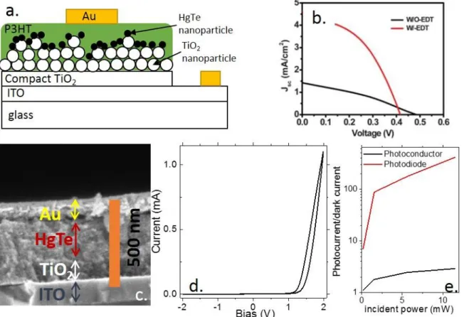
Photovoltaic devices based on HgTe nanocrystals were at first strongly inspired by Gratzel’s solar cell. HgTe nanocrystals were used as dyes to sensitize a porous TiO2 nanoparticle network, see Figure 1a. As the targeted
application was solar cell, the devices were operated with small nanocrystal presenting absorption in the near[7,56] and
short-wave infrared.[57]. The TiO
2 network was used to extract the electrons and the holes were collected thanks to a
P3HT organic transport layer. The obtained diode presents a clear rectifying behavior, see Figure 1b, even though the performances remain weaker than the ones obtained using PbS[58,59] and more recently perovskite nanocrystals.[60]
Moreover, HgTe appears as a poor candidate for solar cell design for obvious toxicity issue. Its use has then been focused on applications where no low toxicity alternatives exist, as this is currently the case in the extended short wave and mid infrared ranges. In the short wave infrared range, the driving technology is based on InGaAs. The road map for InGaAs technology only offers limited perspectives for cost disruption, slowing down the democratization of IR technology for applications such as active imaging (defense, LIDAR detection, material sorting…). Also, InGaAs presents limited spectral tunability which can be easily overcome using quantum confined nanocrystal.
In the recent years, HgTe has been widely used to explore devices with absorption above 2 µm.[34,46,61] Pushing the
nanocrystal absorption toward longer wavelength requires to update the device architecture. In particular organic ligands also absorb in the mid infrared, with resonance of C-H bonds occurring around 3 µm (2900 cm-1). Because of
the near-field coupling of these ligands with the absorption of the inorganic semiconductor, the energy transfer from the nanocrystal to the ligands is strongly efficient and leads to a quenching of the exciton. It is then critical to conduct a ligand exchange step to prevent his energy transfer from the semiconductor exciton to organic ligands. Similarly, the P3HT hole transport layer needs to be replaced
To avoid the use of organic layer, Jagtap et al.[52] have proposed an all inorganic photovoltaic configuration using HgTe
nanocrystals based on the following stack: glass/ITO/TiO2/HgTe/gold, see Figure 1c. Thin ITO layer has to be used to
avoid excessive absorption in the short wave infrared range. The exact value of its thickness is a trade-off between the electrode absorption and the contact resistance. The TiO2 , thanks to its n-type nature,[62] is here to induce the hole
Figure 1d. The signal to noise ratio of the same film of HgTe (i.e. same thickness and surface chemistry) is enhanced by a factor hundred as we switch from a photoconductive configuration to a photovoltaic configuration (see Figure 1e), mostly because of the dark current reduction made possible by the zero volt operation of the diode.
Figure 1 : (a) Cross-sectional sketch of a NIR photovoltaic device, which combines the concepts of a solid-state nanocrystal-sensitized solar cell and a nanocrystal/polymer-blend solar cell. ITO: indium tin oxide. Figure is inspired from ref [57]. (b) I-V curve with and without ethanedithiol treatment for the device of part a. Parts a and b are adapted from ref [7]. (c) Cross sectional SEM image of a HgTe CQD based device in photovoltaic configuration. In this device, HgTe nanocrystals absorb at 2.5 µm. (d). I - V curve of the HgTe CQD device in photovoltaic configuration. (e) Photocurrent over dark current ratio as a function of incident power for a photoconductive device consisting of a film of HgTe nanocrystals between two gold electrodes (Au/HgTe/Au) and for photodiode with an ITO/TiO2/HgTe/Au geometry.
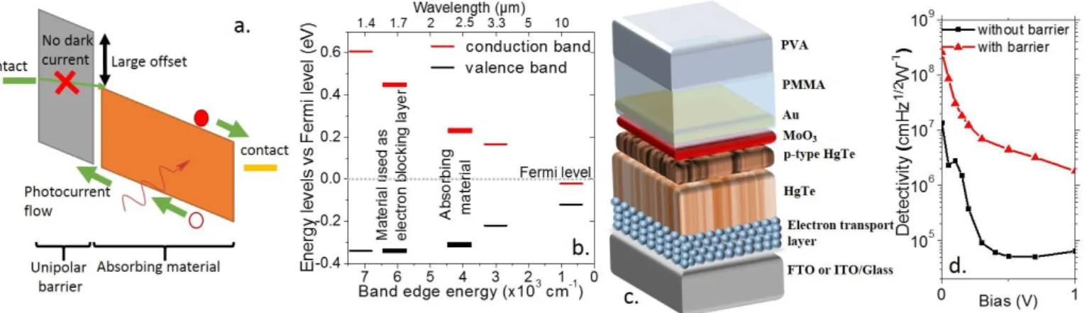
Unipolar barrier
Another interesting concept that has recently been introduced for the design of infrared nanocrystal based photovoltaic devices is unipolar barrier.[63] The basic concept is illustrated in Figure 2a. A barrier layer is introduced
between one contact and the absorbing layer. This layer has a resonant band alignment with the absorbing layer for one type of carrier, which will let photocurrent flow, while it has a clear band offset for the other type of carriers which will prevent the dark current injection.
While this concept is commonly used for III-V semiconductor[64,65] it has only limited development in the field of
nanocrystals. The reason for that is the very limited knowledge of the exact energy of the valence and conduction band states in the case of nanocrystals. This effort has been done in the case of HgTe using a combination of photoemission and IR spectroscopy,[66] see Figure 2b. It appears that the work function is almost independent of the
nanocrystal size and equal to 4.6±0.1 eV. Strongly confined nanocrystals of HgTe show a p-type character which shifts to ambipolar and finally to degenerately n-type as the quantum confinement is reduced. Interestingly, we also observe that confinement affects more strongly the conduction band energy rather than the valence band energy due to the large difference between hole and electron effective masses. This offers an interesting possibility for unipolar barrier
design. Indeed, a layer of strongly confined nanocrystals can be used as unipolar barrier for less confined nanocrystals. Jagtap et al.[66] used this concept in a photovoltaic device operated in the extended short wave infrared range. HgTe
nanocrystals with a band edge at 2.5 µm were used as absorbing layer, while HgTe nanocrystals with a 1.5 µm band-edge were used to filter the electron dark current. The introduction of this layer led to an increase of the detectivity by one order of magnitude compared to the same device without unipolar barrier, see Figure 2c and d.
Figure 2 (a) Schematic of the band diagram for a unipolar barrier used to prevent electron dark current injection. (b) Band alignment of HgTe nanocrystals with different values of band edge energy. In particular, we highlight the weak valence band offset between 4000 cm-1 and 6000 cm-1 band edge energy materials. (c) Schematic of electrically active photodiode including the unipolar barrier. (d) Detectivity as a function of the applied bias for ITO/TiO2/HgTe (ambipolar - 4000 cm-1)/Au and for FTO/TiO
2/HgTe (ambipolar - 4000 cm-1)/HgTe (p-type - 6000 cm-1)/MoO3/Au photodiode.
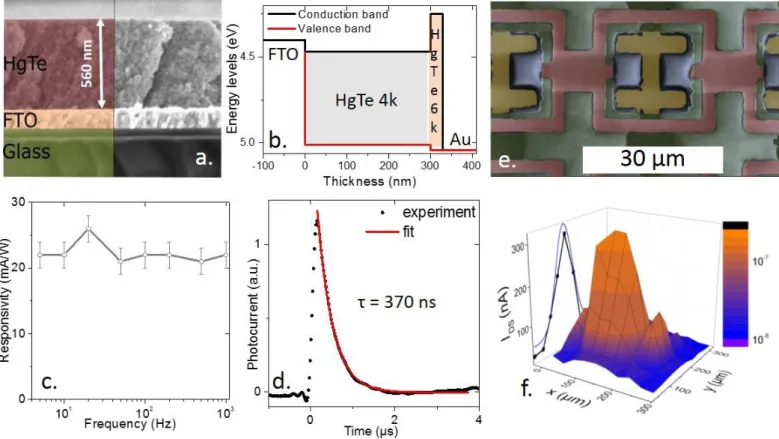
Strongly absorbing film
A key limitation of the previously mentioned devices comes from their low absorption. For a 2.5 µm band edge the absorption coefficient of HgTe nanocrystal is around 3x103 cm-1, which makes that a 200 nm thick layer only absorbs
≈ 10 % of the incident light. In addition, the relatively low mobility of ethanedithiol-capped HgTe nanocrystals makes that the carrier diffusion length is short (10 nm) which makes that building thick film will only lead to marginal improvement of the performance. For nanocrystal-based solar cells, a large effort has been dedicated to switch from solid state ligand exchange to ink (i.e. in-solution ligand exchange).[67–69] This strategy has been made possible thanks
to the introduction of inorganic capping ligands by Talapin’s group.[70,71] This concept was first developed for field
effect transistors and its implementation for IR sensor took several years. Martinez et al.[50] have proposed to use this
concept for HgTe nanocrystals and succeeded to build films with > 500 nm thickness in a single deposition step, see Figure 3a and b, with a diffusion length close to 200 nm. Once combined with a unipolar barrier to filter the dark current, the obtained diode presents responsivity above 20 mA/W at room temperature and zero volt operating bias, see Figure 3c. Time response of such diode has been found to be as short as 370 ns which is quite promising for pulsed active imaging system (LIDAR detection), see Figure 3d. The material was also coated onto the surface of a small focal plane array (FPA) made of 10 x 10 pixels, see Figure 3e. This FPA was used to obtain an infrared laser beam profile, see Figure 3f. Such application looks perfectly suited for nanocrystal based laser sensors since the large photon flux makes that dark current is not limiting the performance.
Figure 3 (a) SEM cross-section of the ink based diode. (b) Band alignment of the different components of the diode. (c) Responsivity under blackbody illumination at 980 °C. (d) Time response of the diode measured with a 355 nm pulsed laser (2 ns pulse). The time response value is obtained through single exponential fitting. (e) SEM image of a matrix pixel with fake colors corresponding to different layers: yellow is the internal gold contact (columns), green is the insulating silica between the two gold electrodes and orange is the external gold contact (lines) (magnified 3000x).(d) Intensity collected by the different pixels while laser spot is focused on the FPA. The Gaussian shape has a FWMH of 75 µm.
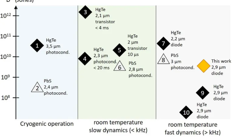
By the time of this article, Tang et al. has reported an impressive bi color photodiode operating in the SWIR and MWIR with detectivity above 1010 Jones at 80 K in both bands.[41] Ourresults can be compared with the ones from literature
Figure 4 : State of the art on SWIR and ESWIR detection based on narrow band gap nanocrystals. The corresponding performances of these devices are reported in Table 1.
Table 1 : State of the art on SWIR and ESWIR detection based on narrow band gap nanocrystals. The numbers in the left column correspond to the data provided in Figure 4.
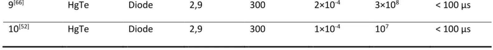
Ref. Material Mode λcutoff
(µm)
Operating temperature (K)
R (A/W) D* (Jones) Time response 1[33] HgTe PC 3,5 230 0,1 3,5×10¹⁰ ≈ 1 µs 2[72] PbS PC 2,4 230 50 @1,5µm 3,4×10 8 40 Hz bandwith 3[61] HgTe Photo-transistor 2,1 300 8×10 2 1012 < 4 ms 4[46] HgTe PC 2,3 300 0,9 8×10⁹ ≈ 20 ms 5[34] HgTe Photo-transistor 2 300 0,6 2×10 10 ≈ 10 µs 6[73] PbS PC 2,8 300 0,96 8×10⁹ Unknown 7[41] HgTe Diode 2,2 300 0,23 7,5×10¹⁰ 260 ns 8[74] PbS PC 3 300 0,14 @2,5µm 1,1×10 10 3 kHz bandwith
9[66] HgTe Diode 2,9 300 2×10⁻⁴ 3×10⁸ < 100 µs
10[52] HgTe Diode 2,9 300 1×10⁻⁴ 107 < 100 µs
Intraband diode
To finish, we would like to mention the recent development of intraband photodiode. Quickly after the observation of the self-doping in mercury chalcogenide nanocrystals, it has been proposed to use this transition for mid wave infrared sensing.[12,75] Arrays of HgSe however suffer from a slow response, a low activation energy (i.e. cooling barely
improves performances) and a large dark current. These issues can be solved either by growing a HgTe shell[19] around
the HgSe absorbing material or by mixing HgSe and HgTe nanocrystals.[76] The strategy behind these approaches is to
uncouple the absorption from the transport. It thus becomes possible to reproduce from colloidal material the energy landscape of Quantum Well and Quantum Dot Infrared detector based on III-V materials, where absorption occurs in the well and charge transport occurs above the barrier, see Figure 5a and b. These hybrid metamaterials present a weak dark current and a strongly accelerated time response, see Figure 5c. The hybrid material was then integrated into the first intraband photodiode obtained from colloidal material. The bottom MWIR-transparent electrode is made from an Al grid deposited on sapphire, see Figure 5d. A unipolar barrier is again used in this device to reduce the dark current. Interestingly, the device presents photocurrent features in the SWIR, extended SWIR and MWIR, which relative magnitude can be tuned with the applied bias, see Figure 5f.
Figure 5 (a) Scheme of a standard GaAs/AlGaAs QWIP band structure under polarization. (b) Scheme of polarized band structure of a random colloidal QDIP consisting of HgSe (absorbing material) and HgTe (barrier) quantum dots. (c) Photocurrent temporal trace for arrays of HgSe with and without addition of HgTe, measured under illumination by a 4.4 µm Quantum Cascade Laser chopped at 100 Hz. (d) Scheme of the device. Illumination is provided from the
back-side through a sapphire substrate and a patterned aluminum electrode allowing 70% of light transmission in the mid wave infrared range. (e) Band alignment diagram of the diode structure. HgTe with a wide bandgap (0.7 eV, in orange) is used as a unipolar barrier to filter injection of dark current into the active HgSe/HgTe layer. (f) Photocurrent spectra measured at 80 K under 0 V and 1 V bias, showing photoresponse coming from the HgSe intraband absorption (green), HgTe transport matrix (brown) and HgTe barrier (orange). The figure is adapted from ref.[76]
CONCLUSION
We have discussed recent developments relative to HgTe nanocrystal-based photodiodes, starting from concept very close to solar cell. Recent improvements rely on the introduction of unipolar barrier, development of HgTe ink to produce thick and conductive film or to the use of intraband absorption in a metamaterial where absorption and charge transport are uncoupled. These new design strategies for colloidal materials have been used to obtain fast, high detectivity (<3x10⁹ Jones at room temperature and above 1010 Jones under cryogenic condition) devices, as well
as multipixel devices.
The absorption/diffusion length trends off appears as a driving parameter for the nanocrystal based device. Future development will either have to identify strategies to reduce the effective absorption depth for example by introducing plasmonic resonator. Early results[36,37,77] in this direction have been obtained. However in this direction it will be
critical to keep loss in metal low. In parallel it appears critical to keep developing new surface chemistry to further extend the diffusion length and also to provide higher material stability.
ACKNOWLEDEGMENTS
EL thanks the support ERC starting grant blackQD (grant n° 756225). We acknowledge the use of clean-room facilities from the “Centrale de Proximité Paris-Centre”. This work has been supported by the Region Ile-de-France in the framework of DIM Nano-K (grant dopQD). This work was supported by French state funds managed by the ANR within the Investissements d'Avenir programme under reference ANR-11-IDEX-0004-02, and more specifically within the framework of the Cluster of Excellence MATISSE and also by the grant IPER-Nano2, Graskop, Copin, Frontal.
Conflict of Interest
The authors declare no conflict of interest.
Keywords
HgTe nanocrystals, infrared detection, photovoltaic device.
REFERENCES
[1] S. V. Kershaw, A. S. Susha, A. L. Rogach, Chem. Soc. Rev. 2013, 42, 3033. [2] H. Lu, G. M. Carroll, N. R. Neale, M. C. Beard, ACS Nano 2019, 13, 939. [3] E. H. Sargent, Adv. Mater. 2005, 17, 515.
[4] E. Lhuillier, P. Guyot-Sionnest, IEEE J. Sel. Top. Quantum Electron. 2017, 23, 6000208. [5] C. Livache, B. Martinez, N. Goubet, J. Ramade, E. Lhuillier, Front. Chem. 2018, 6, 575. [6] M. Green, H. Mirzai, J. Mater. Chem. C 2018, 6, 5097.
[8] M. V. Kovalenko, E. Kaufmann, D. Pachinger, J. Roither, M. Huber, J. Stangl, G. Hesser, F. Schäffler, W. Heiss, J.
Am. Chem. Soc. 2006, 128, 3516.
[9] S. Keuleyan, E. Lhuillier, V. Brajuskovic, P. Guyot-Sionnest, Nat. Photonics 2011, 5, 489. [10] S. E. Keuleyan, P. Guyot-Sionnest, C. Delerue, G. Allan, ACS Nano 2014, 8, 8676.
[11] N. Goubet, A. Jagtap, C. Livache, B. Martinez, H. Portalès, X. Z. Xu, R. P. S. M. Lobo, B. Dubertret, E. Lhuillier, J.
Am. Chem. Soc. 2018, 140, 5033.
[12] E. Lhuillier, M. Scarafagio, P. Hease, B. Nadal, H. Aubin, X. Z. Xu, N. Lequeux, G. Patriarche, S. Ithurria, B. Dubertret, Nano Lett. 2016, 16, 1282.
[13] H. Chen, H. Liu, Z. Zhang, K. Hu, X. Fang, Adv. Mater. 2016, 28, 403. [14] G. Shen, M. Chen, P. Guyot-Sionnest, J. Phys. Chem. Lett. 2017, 8, 2224.
[15] E. Izquierdo, A. Robin, S. Keuleyan, N. Lequeux, E. Lhuillier, S. Ithurria, J. Am. Chem. Soc. 2016, 138, 10496. [16] L. K. Sagar, W. Walravens, J. Maes, P. Geiregat, Z. Hens, J. Phys. Chem. C 2017, 121, 13816.
[17] A. Robin, C. Livache, S. Ithurria, E. Lacaze, B. Dubertret, E. Lhuillier, ACS Appl. Mater. Interfaces 2016, 8, 27122. [18] G. Shen, P. Guyot-Sionnest, Chem. Mater. 2019, 31, 286.
[19] N. Goubet, C. Livache, B. Martinez, X. Z. Xu, S. Ithurria, S. Royer, H. Cruguel, G. Patriarche, A. Ouerghi, M. Silly, B. Dubertret, E. Lhuillier, Nano Lett. 2018, 18, 4590.
[20] K. S. Jeong, Z. Deng, S. Keuleyan, H. Liu, P. Guyot-Sionnest, J. Phys. Chem. Lett. 2014, 5, 1139. [21] J. Kim, D. Choi, K. S. Jeong, Chem. Commun. 2018, 54, 8435.
[22] A. Jagtap, C. Livache, B. Martinez, J. Qu, A. Chu, C. Gréboval, N. Goubet, E. Lhuillier, Opt. Mater. Express 2018, 8, 1174.
[23] C. Wang, M. Shim, P. Guyot-Sionnest, Science 2001, 291, 2390.
[24] J. J. Araujo, C. K. Brozek, D. Kroupa, D. R. Gamelin, Nano Lett. 2018, 18, 3893. [25] A. Sahu, A. Khare, D. D. Deng, D. J. Norris, Chem. Commun. 2012, 48, 5458.
[26] S. B. Hafiz, M. R. Scimeca, P. Zhao, I. J. Paredes, A. Sahu, D.-K. Ko, ACS Appl. Nano Mater. 2019, 2, 1631.
[27] J. Qu, N. Goubet, C. Livache, B. Martinez, D. Amelot, C. Gréboval, A. Chu, J. Ramade, H. Cruguel, S. Ithurria, M. G. Silly, E. Lhuillier, J. Phys. Chem. C 2018, 122, 18161.
[28] M. Park, D. Choi, Y. Choi, H. Shin, K. S. Jeong, ACS Photonics 2018, 5, 1907. [29] H. Liu, S. Keuleyan, P. Guyot-Sionnest, J. Phys. Chem. C 2012, 116, 1344. [30] M. Chen, P. Guyot-Sionnest, ACS Nano 2017, 11, 4165.
[31] B. Martinez, C. Livache, L. D. Notemgnou Mouafo, N. Goubet, S. Keuleyan, H. Cruguel, S. Ithurria, H. Aubin, A. Ouerghi, B. Doudin, E. Lacaze, B. Dubertret, M. G. Silly, R. P. S. M. Lobo, J.-F. Dayen, E. Lhuillier, ACS Appl. Mater.
Interfaces 2017, 9, 36173.
[32] B. Martinez, C. Livache, E. Meriggio, X. Z. Xu, H. Cruguel, E. Lacaze, A. Proust, S. Ithurria, M. G. Silly, G. Cabailh, F. Volatron, E. Lhuillier, J. Phys. Chem. C 2018, 122, 26680.
[33] E. Lhuillier, S. Keuleyan, P. Zolotavin, P. Guyot-Sionnest, Adv. Mater. 2013, 25, 137.
[34] M. Chen, H. Lu, N. M. Abdelazim, Y. Zhu, Z. Wang, W. Ren, S. V. Kershaw, A. L. Rogach, N. Zhao, ACS Nano 2017,
11, 5614.
[35] C. Gréboval, U. Noumbe, N. Goubet, C. Livache, J. Ramade, J. Qu, A. Chu, B. Martinez, Y. Prado, S. Ithurria, A. Ouerghi, H. Aubin, J.-F. Dayen, E. Lhuillier, Nano Lett. 2019, DOI 10.1021/acs.nanolett.9b01305.
[36] X. Tang, M. M. Ackerman, P. Guyot-Sionnest, ACS Nano 2018, 12, 7362.
[37] M. Chen, L. Shao, S. V. Kershaw, H. Yu, J. Wang, A. L. Rogach, N. Zhao, ACS Nano 2014, 8, 8208. [38] X. Tang, G. F. Wu, K. W. C. Lai, J Mater Chem C 2017, 5, 362.
[39] Y. Yifat, M. Ackerman, P. Guyot-Sionnest, Appl. Phys. Lett. 2017, 110, 41106. [40] E. Lhuillier, A. Robin, S. Ithurria, H. Aubin, B. Dubertret, Nano Lett. 2014, 14, 2715. [41] X. Tang, M. M. Ackerman, M. Chen, P. Guyot-Sionnest, Nat. Photonics 2019, 13, 277. [42] X. Tang, X. Tang, K. W. C. Lai, ACS Photonics 2016, 3, 2396.
[43] S. V. Kershaw, S. Kalytchuk, O. Zhovtiuk, Q. Shen, T. Oshima, W. Yindeesuk, T. Toyoda, A. L. Rogach, Phys. Chem.
Chem. Phys. 2014, 16, 25710.
[44] A. Al-Otaify, S. V. Kershaw, S. Gupta, A. L. Rogach, G. Allan, C. Delerue, D. J. Binks, Phys. Chem. Chem. Phys. 2013,
15, 16864.
[45] C. Livache, N. Goubet, B. Martinez, A. Jagtap, J. Qu, S. Ithurria, M. G. Silly, B. Dubertret, E. Lhuillier, ACS Appl.
Mater. Interfaces 2018, 10, 11880.
[46] M. E. Cryer, J. E. Halpert, ACS Photonics 2018, 5, 3009.
[47] X. Tang, M. M. Ackerman, G. Shen, P. Guyot‐Sionnest, Small 2019, 15, 1804920.
[48] C. Buurma, R. E. Pimpinella, A. J. Ciani, J. S. Feldman, C. H. Grein, P. Guyot-Sionnest, Opt. Sens. Imaging Photon
[49] A. J. Ciani, R. E. Pimpinella, C. H. Grein, P. Guyot-Sionnest, Proc SPIE Infrared Technol. Appl. XLII 2016, 9819, 981919.
[50] B. Martinez, J. Ramade, C. Livache, N. Goubet, A. Chu, C. Gréboval, J. Qu, W. L. Watkins, L. Becerra, E. Dandeu, J. L. Fave, C. Méthivier, E. Lacaze, E. Lhuillier, Adv. Opt. Mater. 2019, 1900348.
[51] M. Chen, H. Yu, S. V. Kershaw, H. Xu, S. Gupta, F. Hetsch, A. L. Rogach, N. Zhao, Adv. Funct. Mater. 2014, 24, 53. [52] A. Jagtap, N. Goubet, C. Livache, A. Chu, B. Martinez, C. Greboval, J. Qu, E. Dandeu, L. Becerra, N. Witkowski, S.
Ithurria, F. Mathevet, M. G. Silly, B. Dubertret, E. Lhuillier, J. Phys. Chem. C 2018, 122, 14979. [53] H. Liu, E. Lhuillier, P. Guyot-Sionnest, J. Appl. Phys. 2014, 115, 154309.
[54] P. Guyot-Sionnest, J. A. Roberts, Appl. Phys. Lett. 2015, 107, 253104. [55] M. M. Ackerman, X. Tang, P. Guyot-Sionnest, ACS Nano 2018, 12, 7264. [56] S. Hyuk Im, H. Kim, S. Woo Kim, S.-W. Kim, S. Il Seok, Nanoscale 2012, 4, 1581.
[57] S. Günes, H. Neugebauer, N. S. Sariciftci, J. Roither, M. Kovalenko, G. Pillwein, W. Heiss, Adv. Funct. Mater. 2006,
16, 1095.
[58] C.-H. M. Chuang, P. R. Brown, V. Bulović, M. G. Bawendi, Nat. Mater. 2014, 13, 796.
[59] K. Lu, Y. Wang, Z. Liu, L. Han, G. Shi, H. Fang, J. Chen, X. Ye, S. Chen, F. Yang, A. G. Shulga, T. Wu, M. Gu, S. Zhou, J. Fan, M. A. Loi, W. Ma, Adv. Mater. 2018, 30, 1707572.
[60] A. Swarnkar, A. R. Marshall, E. M. Sanehira, B. D. Chernomordik, D. T. Moore, J. A. Christians, T. Chakrabarti, J. M. Luther, Science 2016, 354, 92.
[61] N. Huo, S. Gupta, G. Konstantatos, Adv. Mater. 2017, 29, 1606576.
[62] W. Ouyang, F. Teng, J.-H. He, X. Fang, Adv. Funct. Mater. 2019, 29, 1807672. [63] P. Martyniuk, M. Kopytko, A. Rogalski, Opto-Electron. Rev. 2014, 22, 127.
[64] G. R. Savich, J. R. Pedrazzani, D. E. Sidor, G. W. Wicks, Infrared Phys. Technol. 2013, 59, 152.
[65] G. R. Savich, J. R. Pedrazzani, D. E. Sidor, S. Maimon, G. W. Wicks, Appl. Phys. Lett. 2011, 99, 121112.
[66] A. Jagtap, B. Martinez, N. Goubet, A. Chu, C. Livache, C. Gréboval, J. Ramade, D. Amelot, P. Trousset, A. Triboulin, S. Ithurria, M. G. Silly, B. Dubertret, E. Lhuillier, ACS Photonics 2018, 5, 4569.
[67] Z. Ning, H. Dong, Q. Zhang, O. Voznyy, E. H. Sargent, ACS Nano 2014, 8, 10321.
[68] A. Fischer, L. Rollny, J. Pan, G. H. Carey, S. M. Thon, S. Hoogland, O. Voznyy, D. Zhitomirsky, J. Y. Kim, O. M. Bakr, E. H. Sargent, Adv. Mater. 2013, 25, 5742.
[69] D. M. Balazs, N. Rizkia, H.-H. Fang, D. N. Dirin, J. Momand, B. J. Kooi, M. V. Kovalenko, M. A. Loi, ACS Appl. Mater.
Interfaces 2018, 10, 5626.
[70] A. Nag, M. V. Kovalenko, J.-S. Lee, W. Liu, B. Spokoyny, D. V. Talapin, J. Am. Chem. Soc. 2011, 133, 10612. [71] M. V. Kovalenko, M. Scheele, D. V. Talapin, Science 2009, 324, 1417.
[72] C. Hu, A. Gassenq, Y. Justo, K. Devloo-Casier, H. Chen, C. Detavernier, Z. Hens, G. Roelkens, Appl. Phys. Lett. 2014, 105, 171110.
[73] M. Thambidurai, Y. Jang, A. Shapiro, G. Yuan, H. Xiaonan, Y. Xuechao, Q. J. Wang, E. Lifshitz, H. V. Demir, C. Dang,
Opt. Mater. Express 2017, 7, 2326.
[74] N. Killilea, M. Wu, M. Sytnyk, A. A. Y. Amin, O. Mashkov, E. Spiecker, W. Heiss, Adv. Funct. Mater. 2019, 29, 1807964.
[75] Z. Deng, K. S. Jeong, P. Guyot-Sionnest, ACS Nano 2014, 8, 11707.
[76] C. Livache, B. Martinez, N. Goubet, C. Gréboval, J. Qu, A. Chu, S. Royer, S. Ithurria, M. G. Silly, B. Dubertret, E. Lhuillier, Nat. Commun. 2019, 10, 2125.
![Aflatoxin B[subscript 1]-DNA adduct formation and mutagenicity in livers of neonatal female B6C3F1 mice](data:image/gif;base64,R0lGODlhAQABAIAAAP///wAAACH5BAEAAAAALAAAAAABAAEAAAICRAEAOw==)