Chapter 3. Computer-Assisted Prototyping of Advanced Microsystems
Chapter 3.
Computer-Assisted Prototyping of Advanced
Microsystems
Academic and Research Staff
Professor Dimitri A. Antoniadis, Professor Duane S. Boning, Professor Anantha P. Chandrakasan, Professor Carl V. Thompson, Professor Donald E. Troxel, Thomas J. Lohman, Michael B. Mcllrath
Graduate Students
Yonald Chery, Aaron E. Gower, Brian Lee, Zachary Lee, William P. Moyne, Manuel Perez, Debashis Saha, Matthew D. Verminski
Technical and Support Staff Francis M. Doughty
3.1 Advanced Modeling and
Computational Prototyping
SponsorDefense Advanced Research Projects Agency Contract DABT 63-95-C-0088
3.1.1 Modeling of Interconnect Reliability Project Staff
Yonald Chery, Professor Carl V. Thompson, Profes-sor Donald E. Troxel
Recent research has demonstrated interconnect fail-ure due to electromigration effect to be strongly dependent not only on current density but also on metal film crystal grain size distribution and geome-tries of interconnect patterns. This type of failure is manifest as a depletion of interconnect metal forming a "void" (open-circuit) or an accumulation possibly forming a "short" to neighboring interconnect.
Our research work focuses on:
1. Developing abstract, physically-based, micro-structural interconnect failure models to more accurately predict electromigration induced failure.
2. Electromigration Reliability for Network Inter-connect (ERNI), our prototype computer-aided design tool based on these abstracted micro-structurally based models.
1 N. Khalil et al., IEEE Electron Device Lett. 16 (1): 17 (1995). 2 G.J.L. Ouwerling,Solid State Electron. 34(2): 197 (1991).
A release of ERNI 2.0 is expected during spring 1998 with extensions supporting hierarchical designs and utilizing higher performance circuit simulation engines. This release will incorporate client and server programs implemented in Java. With this, multiple designers at different locations will be able to cooperatively design integrated circuitry which incor-porates electromigration reliability models.
3.1.2 Modeling of Advanced Device Structures
Project Staff
Zachary Lee, Michael B. Mcllrath, Professor Dimitri A. Antoniadis
As MOS transistors are scaled to the submicron regime, the two-dimensional (2D) distribution of dopants becomes a very important factor affecting their performance. A technique that allows one to obtain the doping profile is therefore indispensable. One-dimensional (1D) profiling techniques such as the C-V method and SIMS have widely been used. Direct 2D techniques, however, have met with less success. Khalil et al.1 and Ouwerling2 used an inverse modeling approach by finding a doping pro-file such that its simulated C-V characteristics match
its corresponding experimentally determined coun-terpart.
We have developed a new inverse modeling-based technique for the extraction of 2D doping profiles in submicron MOS transistors using I-V characteristics
Chapter 3. Computer-Assisted Prototyping of Advanced Microsystems
in the subthreshold region. The main advantages of this technique include: (1) ability to extract 2D doping profiles of devices having very short channel lengths due to its immunity to parasitic capacitances and noise; (2) low sensitivity to gate area variations; (3) low dependence on mobility model; (4) nondestruc-tive nature; and (5) simplicity of data collection and preparation, as well as general ease of use.
In general, the I-V data of a short-channel device in the subthreshold region capture the 2D electrostatic effects of drain-induced barrier lowering (DIBL), sub-surface punch- through, sub-surface punch-through, and subthreshold slope. For example, the DIBL effect results from the reduction in surface potential energy barrier between the source and channel due to the built-in potential and applied bias (Vds) at the drain. According to the analytical model of Liu et al.,' the shift in threshold voltage (Vth) has an approximate lin-ear dependence on Vds, and an exponential depen-dence on the 2D doping geometry (in particular, the
"channel length" Lch). The corresponding change in drain current (Id) is therefore exponentially depen-dent upon Vds, and also exponentially dependepen-dent upon the exponential of the doping geometry. On the other hand, Id depends only linearly on the mobility
(m) and device geometry such as the width (W) and gate length (Lg). Consequently the uncertainty of m and gate area is not significant in the profile extrac-tion, in light of the much greater dependencies that the current has on the 2D distribution of dopants as signified by the 2D effects discussed above. Similar to DIBL, the subthreshold slope and extent of punch-through also provide important information.
We have demonstrated the application of the tech-nique on a number of devices having different chan-nel dopings, but similar source/drain dopings with indium "halo" implants.4 The extraction procedure starts with the extraction of the 1 D doping profile (i.e., doping in the depth direction), which can be accom-plished by fitting Id versus Vgs versus Vbs data of a long-channel device, the C-V method of a large area capacitor, or from SIMS data.
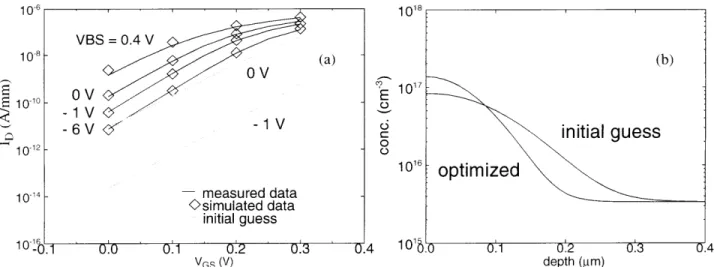
Figure la shows the I-V data of a device having a step-doping channel pro file as shown in Figure lb.
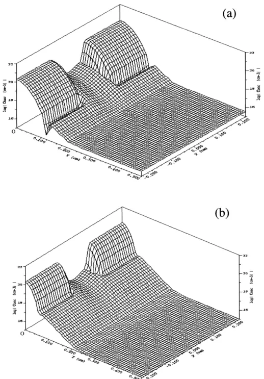
Here, the profile is represented by a sum of two Gaussian functions, with the amplitude, center, and width of each Gaussian function a fitting parameter. Once the 1D profile is obtained, the 2D profile, as parameterized using a sum of two 2D Gaussian func-tions, and representing the source/drain/halo re-gions, is extracted by fitting simulated Id versus Vgs versus Vds data generated by the device simulator MEDICI5 to the corresponding experimental data in the subthreshold region. Here, the center and width of each Gaussian function, in both the depth and lat-eral directions, are varied in the optimization. The amplitude of one of the Gaussian functions, which represents the "halo" doping, is also allowed to be optimized. The amplitude of the second Gaussian function, which represents the source/drain, how-ever, is kept fixed at the doping level as determined by 1D process simulations and SIMS, since the tech-nique is unable to resolve very high (i.e., degenerate) doping levels.
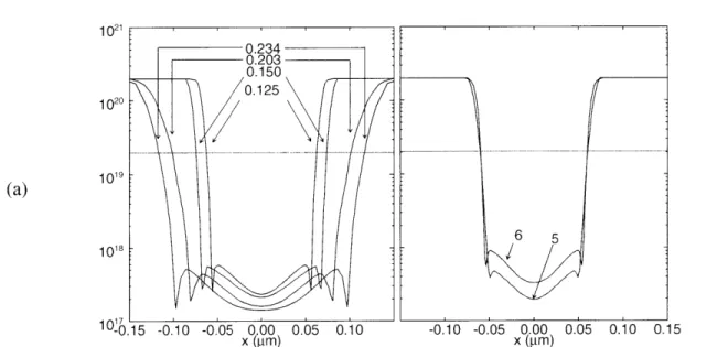
Figure 2 shows the I-V data of the initial and opti-mized profiles as shown in Figure 3a and Figure 3b, respectively. Figure 4a and Figure 4b show a com-parison between the extracted profiles of different devices. It can be seen that the source/drain/halo regions of the devices are very similar, particularly the peak doping levels of the "halo" implants, which occur at approximately 1018 cm-3. This is an expected result since the devices were processed under simi-lar conditions.
3 Z. Liu et al., IEEE Trans. Electron Dev. 40(1): 86 (1993). 4 H. Hu et al., IEEE Trans. Electron Dev. 42: 669 (1995). 5 MEDICI Manual, Technology Modeling Associates.
Chapter 3. Computer-Assisted Prototyping of Advanced Microsystems 10-', 10 VBS = 0.4 V 108 ,-,q>" ,,--/ OV - (a) , (b) 0 V 1017 10-10 S -1Vo 0 1016
optimized
10-14 - measured data Osimulated data initial guess 10 _. 1 0.0 0.1 0.2 0.3 0.4 1016.0 0.1 0.2 0.3 VGS (V) depth (pm)Figure 1. (a) Comparison of measured, simulated (initial guess), and simulated (optimized) data of the 1D (depth) profiles as shown in (b). The device has Lgate = 5 lm, with Tox = 50 A, W = 50 ptm, and a step-doping channel profile formed by BF2 implants.
10-4 10-6 10-8 10-10 1012 1014 1 0 -16 -0.6- -0.4 -0.2 0.0
VGS (V)
0.2 0.4 0.6 0.2 0.4 0.6Figure 2. Measured, simulated (initial guess), and simulated (optimized) data of a device having the step-doping channel profile of Figure 1 b, and a nominal Lgate = 0.15 tm, Tox = 50 A, W = 5 tm, and with "halo" source/drain implants. The source and drain were formed by arsenic while the "halos" were formed by indium implants. 309 (a) VDS = 2.01 V
1.01 V
0.21
V-0.01 V
-
measured data
0
simulated data
S....initial
guess
SI I I I I IChapter 3. Computer-Assisted Prototyping of Advanced Microsystems
Figure 3. (a) initial guess profile used in the extraction shown by Figure 2. Note the large junction depths that caused the large amounts of punch-through. (b) optimized profile having I-V characteristics that match the
measured data.
By obtaining the 2D doping profile, this technique automatically allows one to obtain the channel length, which is an important parameter for gauging technologies. Figure 4 shows a comparison between
6 C. Huang et al., IEEE Trans. Electron Dev. 43(6): 958 (1996).
the extracted channel lengths using this technique with the effective channel lengths extracted using the C-V and the "shift and ratio" methods.6 Here, the channel length is "defined" by the positions in the
310 RLE Progress Report Number 140
_ ~ __ ~__ __ ~~=
--Chapter 3. Computer-Assisted Prototyping of Advanced Microsystems
source/drain at which the doping is sufficiently high (i.e., 2x1019cm3, although due to the steepness of the source/drain profiles this value is not critical.) The agreement is very good. It should be noted that the Gaussian representation presented here is only one of many possibilities; other functions such as the complementary error function and spline representa-tions may be used as well. Further development of the technique may involve matching both I-V and C-V data simultaneously to make use of the best of both techniques.
Table 1 is a comparison of Leff of various devices extracted by the Cgds and shift and ratio methods7 and the inverse modeling technique presented in this report. The numbers given in the first column corre-spond to the same numbers designated for the devices of Figure 4.
1021
1020
1018
1017
Table 1: Comparison of Leff Leff (pm)
Inverse
Device No. Cgds method Modeling
1 0.122 0.125 2 0.162 0.150 3 0.203 0.203 4 0.232 0.234 -0.10 -0.05 0.00 0.05 0.10 0.15 x (pm)
Figure 4. Comparison of lateral doping profiles at the SiO2/Si interface of various devices. Other than the
channel implant and Lgate, the devices are identical (i.e., having the same source/drain/halo implants.) (1) device having the step channel doping of Figure lb and a nominal Lgate = 0.15 tm; (2)-(4) same as (1), but respectively having Lgate = 0.19 ptm, 0.23 pm, and 0.26 ptm; (5) device having no channel implant, with Lgate =
0.15 pLm; (6) device having a super-steep retrograde channel profile, with Lgate = 0.12 ptm. Note that at degenerate doping levels (i.e., 2x1019cm-3), as within the region indicated by the dashed line, the accuracy of the extracted profiles decreases.
7 C. Huang et al., IEEE Trans. Electron Dev. 43(6): 958 (1996).Ibid.
Chapter 3. Computer-Assisted Prototyping of Advanced Microsystems
3.1.3 Conference Papers
Lee, Z., M. Mcllrath, and D. Antoniadis. "Inverse Modeling of MOSFETs using I-V Characteristics in the Subthreshold Region." Proceedings of the International Electron Devices Meeting (IEDM), Washington, D.C., December 1997.
3.2 Distributed Collaborative Design
and Prototyping Infrastructure
SponsorsDefense Advanced Research Projects Agency Contract DABT 63-95-C-0088
Stanford University
3.2.1 Architecture for Distributed Design and Fabrication
Project Staff
Professor Duane S. Boning, Michael B. Mcllrath, Professor Donald E. Troxel
The design and fabrication of state-of-the-art semi-conductor devices and integrated circuits requires an increasingly diverse and expensive set of resources, including manufacturing equipment, people, and
computational tools. Advanced semiconductor
research activities can be even more demanding, fre-quently requiring unique equipment and processing capabilities.
We are developing a flexible, distributed system architecture capable of supporting collaborative design and fabrication of semiconductor devices and integrated circuits. Such capabilities are of particular importance in the development of new technologies, where both equipment and expertise are limited. Dis-tributed fabrication enables direct, remote, physical experimentation in the development of leading edge technology, where the necessary manufacturing resources are new, expensive, and scarce. Compu-tational resources, software, processing equipment, and people may all be widely distributed; their effec-tive integration is essential in order to achieve the realization of new technologies for specific product requirements. Our architecture leverages current vendor and consortia developments to define soft-ware interfaces and infrastructure based on existing and emerging networking, CIM, and CAD standards. Process engineers and product designers access
processing and simulation results through a common interface and collaborate across the distributed man-ufacturing environment.
3.2.2 Labnet Software Project Staff
Thomas L. Lohman, Professor Duane S. Boning University microfabrication laboratories are facing many new challenges and opportunities: (1) facilities are becoming more expensive and difficult to man-age; (2) resources and expertise need be shared and made available to a wider community; and (3) educa-tion and research are becoming more dependent on multi-institutional collaboration. Given the above challenges, there is a growing need for a new distrib-uted information infrastructure, that will allow remote collaboration, access to remote sites' data and shar-ing of end-user software applications, considershar-ing the differences between remote sites in computer
platforms, operating systems, and technical
resources. Past research has been done within this application domain but most working systems are too tightly coupled to their local facilities, suffer from port-ability problems, and do not address the issue of
data distribution and remote site interaction.
The Labnet Software Project was initiated in recogni-tion of a need for universities to share the develop-ment and support effort needed to develop and maintain new distributed laboratory information sys-tems. Joint development work among MIT, Stanford University and the University of California at Berkeley is in progress. The main goals of the joint develop-ment effort are to:
* Assess the applicability of emerging technologies such as the Object Management Group's (OMG) Common Object Request Broker Architecture
(CORBA), OMG's Interface Definition Language (IDL), Sun Microsystem's Java language, and object databases.
* Explore infrastructure to enable collaborative dis-tributed design and fabrication (including object-oriented distributed programming interfaces and web-based user interface capability).
* Develop abstract specifications of programming interfaces to both data and services.
* Explore standards to achieve software compatibil-ity such as the Sematech CIM Application Frame-work.
Chapter 3. Computer-Assisted Prototyping of Advanced Microsystems
Publication
Mcllrath, M., D.S. Boning, and D.E. Troxel. "Architec-ture for Distributed Design and Fabrication." In Plug and Play Software for Agile Manufacturing. Ed. B.L.M. Goldstein. Proc. SPIE 2913: 134-47 (1997).
3.2.3 Distributed Process Control Architecture
Project Staff
Aaron E. Gower, Professor Duane S. Boning, Michael B. Mcllrath
Semiconductor fabrication requires an increasingly expensive and integrated set of tightly controlled pro-cesses, driving the need for a fabrication facility with fully computerized, networked processing equip-ment. We have designed an integrated, open system architecture enabling distributed experimentation and process control for plasma etching. The system was developed at MIT's Microsystems Technology Labo-ratories and employs in-situ CCD interferometry based analysis in the sensor-feedback control of an Applied Materials Precision 5000 Plasma Etcher
(AME5000). Our system supports accelerated,
advanced research involving feedback control algo-rithms and includes a distributed interface that uti-lizes the internet to make these fabrication capabilities available to remote users.
The system architecture is both distributed and mod-ular: specific implementation of any one task does not restrict the implementation of another. The low level architectural components include a host control-ler that communicates with the AME5000 equipment via SECS-Il and a host controller for the acquisition and analysis of the CCD sensor images. A Cell
Con-troller (CC) manages communications between
these equipment and sensor controllers. The CC is also responsible for process control decisions; algo-rithmic controllers may be integrated locally or via remote communications. Finally, a System Server manages connections from internet/intranet (web) based clients and uses a direct link with the CC to access the system. Each component communicates via a predefined set of TCP/IP socket based mes-sages. This flexible architecture makes integration easier and more robust and enables separate soft-ware components to run on the same or different computers independent of hardware or software plat-form.
Publication
Gower, A., D. Boning, and M. Mcllrath. "Flexible, Dis-tributed Architecture for Semiconductor Process Control and Experimentation." In Open Architec-ture Control Systems and Standards. Ed. F.M. Proctor; Proc. SPIE 2912: 146-58 (1997).
3.2.4 Remote Microscope for Collaborative Inspection of Integrated Circuits Project Staff
Manuel Perez, Brian Lee, Professor Donald E. Troxel The internet remote microscope was developed to enable users to inspect a microscope specimen remotely by using an ordinary workstation computer connected to the internet. The remote microscope is a distributed system that consists of one or more graphical client interfaces that communicate over the internet with a microscope server unit consisting of hardware and software needed to automatically con-trol an inspection microscope. The client interface presents the user with a graphical microscope control panel and two image panels that show static images of the microscope specimen that can be updated upon request.
Because it is not important to have live video when examining many types of specimens, especially in the context of inert semiconductor wafers, this approach gives acceptable performance while requir-ing only limited bandwidth. From the control or instru-mentation panel, the user may select a new magnification, pan position, and focus setting (man-ual or automatic), and can then instruct the system to capture a new image at the specified coordinates. The new image can be placed in one of the two arbi-trary display windows, allowing the user to keep a
previous image for reference. Typically, one would actually use one window to show a global or pan-oramic view of the specimen at low magnification, while using the other window to show a more detailed region of interest at high magnification. The server system consists of a Zeiss microscope, an auto-mated stage accurate to 0.4 microns for X-Y transla-tion and 0.1 microns for Z directransla-tion, a video camera, and an ordinary personal computer running OS/2 that services requests over the internet from clients. The PC contains a framegrabber board that can cap-ture an ordinary NTSC video signal from a CCD cam-era that is mounted on top of the microscope, and the PC is also responsible for controlling the stage,
Chapter 3. Computer-Assisted Prototyping of Advanced Microsystems
ret, and focus settings for an automated Zeiss micro-scope. Except for the initial placement of a wafer on the stage, this system is fully automated and control-lable from the client control panel. Essentially, the remote microscope allows distant users to access and view a specimen remotely as if they were con-trolling the microscope themselves. An additional capability of the internet remote microscope is that multiple clients can view the microscope simulta-neously during a conference inspection mode. This enables any number of experts anywhere on the internet to simultaneously view the microscope images collaboratively, although only one person at a time is in control and allowed to change the system settings.
Users use the remote microscope by retrieving the client applet from a web server, residing on the same system as the remote microscope server application. This design has made the client program platform independent, allowing the use of the client on any machine which supports Java applets. The Java cli-ent currcli-ently includes all the functionality of the origi-nal client, as well as many of the new manual focusing options currently being designed.
New features added include a text chat tool, online help files, a mini tools window, and a layout based navigation tool. The text based chat tool allows users to send small text messages to one another, while inspecting a wafer. The online help contains a com-plete users guide, trouble shooting tips, and other remote microscope related material. These help files will be directly available through the web server. The mini tools window allows for quick zoom, move, and grab commands, as well as including some measure-ment functions. A Java based MAGIC file viewer in our group serves as the basis for an easy and quick navigation tool.
Publication
Perez, M. Java Remote Microscope for Collaborative Inspection of Integrated Circuits. M.Eng. thesis, Department of Electrical Engineering and Com-puter Science, MIT, June 1997.
3.2.5 Semiconductor Process Repository Project Staff
Matthew D. Verminski, William P. Moyne, Michael B.
Mcllrath, Professor Donald E. Troxel
The goal of this research task is to create a system to facilitate distributed process research and design. Such a system will allow users to retrieve and exam-ine process flows from multiple process libraries across the network.
Work has proceeded on the design and development of a distributed process repository interface. The repository application programming interface (API) is
encapsulated by an OMG CORBA distributed object model and defined by an Interface Description Lan-guage (IDL) specification. The process object model used to encapsulate the process repository API is based on the Semiconductor Process Representa-tion (SPR) InformaRepresenta-tion Model. The IDL specification is programming language-neutral; application clients and repository services may be implemented in any language supported by a CORBA-compliant object request broker (ORB) and interoperate across a local or wide-area network. Process repositories may be distributed; process objects and services may be located at various sites transparently to application clients. Applications and services may interoperate using entirely distinct ORB implementations if a com-mon protocol such as the Internet InterORB Protocol
(IIOP) or appropriate bridges are available.
The present SPR IDL development includes the base information model. This standard process represen-tation interface provides a common facility to commu-nicate fabrication processes. The fabrication process
information organizes processes into smaller subpro-cesses. At each level, the process can be described from different views. These include the effect of a process on the wafer, the environment around the wafer during the process, and the equipment settings during the process. Each view contains parameters that describe some aspect of the wafer, environment, or equipment during some interval of time. Dynamic attributes (property lists) are also supported for maxi-mum extensibility. The base SPR IDL has been extended to include specific effects and parameters with statistical information.
Two SPR-based repository implementations are in progress. One uses the Xerox InterLanguage Unifi-cation (ILU) ORB8to provide an SPR wrapper to
Chapter 3. Computer-Assisted Prototyping of Advanced Microsystems
cesses in the MIT CAFE CIM system9 used by the Microsystems Technology Laboratories. Repository object implementations are built directly on the CAFE GESTALT object oriented programming layer. This repository implementation now integrates IIOP directly, supporting operation with clients using heter-ogeneous ORBs without the need for the request-level bridging employed earlier.
A distributed software architecture for semiconductor process design has been defined and implemented in Java with the OrbixWeb Object Request Broker (ORB). The implementation communicates with any ORB adhering to the Internet Inter-ORB Protocol
(IIOP). A persistent storage mechanism has been implemented using object design objectstore PSE (Persistent Storage Engine) for Java.
Other services to manage, query and find distributed objects are being developed. Their interfaces are based upon the Object Management Group's (OMG) CORBA services specifications. A Life Cycle service for creating, deleting, copying, and moving distrib-uted objects has been developed. Work has begun on implementing a Query service and a Trader ser-vice. Together, the services will be essential for the development of distributed and shared applications for semiconductor process research and design. We have also been collaborating with the Sematech CIM Framework project in the areas of Specification Management and CIM Architecture. This work is also CORBA IDL-based and we are investigating the pos-sibilities for interoperation of these environments. Thesis
Verminski, M. A Distributed Software Architecture for Semiconductor Process Design. S.M. thesis, Department of Electrical Engineering and Com-puter Science, MIT, January 1998.
3.2.6 Networked and Distributed CAD Tools The rapid growth of computer networks has changed the way applications can be made available. The internet provides a framework with which to distribute and share tools among many users. One of the vari-ous methods used to integrate applications with the internet is the use of CGI (Common Gateway
Inter-face) programming. This complemented with HTML (Hypertext Markup Language) form based entry for inputs allows users with a standard web browser to access applications.
Exploring Semiconductor Device Parameter Space using Rapid Analytical Modeling Project Staff
Brian Lee, Michael B. Mcllrath, Professor Duane S. Boning, Professor Donald E. Troxel, Professor Anan-tha P. Chandrakasan
The creation and implementation of a semiconductor device parameter space exploration tool has been accomplished, which can assist circuit and device designers. Such a tool allows the designer to ana-lyze trade-offs between parameter variations (after defining electrical constraints at the circuit level of abstraction) as well as receive information about fea-sible device structures. In addition, it is also posfea-sible to compare device parameter variations within a technology family, as well as across different technol-ogy families.
The technique of exploring parameter space utilizes a method of rapid analytical modeling to allow for faster, but less accurate, evaluations than one might get through established methods of numerical
simu-lation tools such as MEDICI or PISCES, offering an alternative to such simulators for circuit designers who wish to have rough estimates of parameter vari-ation informvari-ation, or device structure feasibility. The tool can be a valuable addition to any circuit or device designer's CAD environment.
A Framework for Distributed Web-based Microsystem Design
Project Staff
Debashis Saha, Professor Anantha P. Chandrakasan The increasing complexity of microsystem design mandates a distributed and collaborative design environment. The high integration levels call for tools and generators that allow exploration of the design space irrespective of the geographical or physical availability of the design tools.
B. Janssen and M. Spritzer, ILU Reference Manual, Palo Alto Research Center, (Palo Alto: Xerox Corp, 1996).
M.B. McIlrath, D.E. Troxel, M.L. Heytens, P. Penfield, Jr., D.S. Boning, and R. Jayavant, "CAFE-The MIT Computer-Aided Fabrica-tion Environment," IEEE Trans. Comp., Hybrids, Manuf Tech., 15(2): 353-60 (1992).
Chapter 3. Computer-Assisted Prototyping of Advanced Microsystems
The World Wide Web serves as a desirable platform for distributed access to libraries, models and design tools. The rapid growth and acceptance of the World Wide Web has happened over the same time period in which distributed object systems have stabilized and matured. The Web can become an important platform for VLSI CAD, when the distributed object technologies (e.g, CORBA) are combined with the Web technologies (e.g., HTTP, CGI) and Web-aware object oriented languages (e.g., Java).
A framework using the Object-Web technologies enables distributed Web based CAD. The Object-Web architecture provides an open, interoperable and scalable distributed computing environment for microsystem design, in which Web based design tools can efficiently utilize the capabilities of existing design tools on the Web to build hierarchical Web tools. The framework includes the infrastructure to store and manipulate design objects, protocols for tool communication and WebTop, a Java hierarchical schematic/block editor with interfaces to distributed Web tools and cell libraries.
3.3 Scheduling Language for
Manufacturing Systems
We have proposed the syntax and supporting struc-ture of a language that allows a programmer to devise and implement scheduling policies for manu-facturing systems. In the course of the description of the language, we have defined various methods of representing a factory, including the equipment and personnel in the factory, the process flows of parts and constraints on the production of parts.
We take an object-oriented approach to the defini-tions of the various components of the factory model. With the factory well-defined, we have then described the structure and syntax of a language that allows for the implementation of scheduling policies such as Kanban and CONWIP. A running example of a five-machine production line has been used to illus-trate the constructs defined. Finally, we have described the structure of a scheduler based on the constructs developed that takes a real-time control perspective.
Thesis
Nemec, J.E. A Quantity Scheduling Language for Manufacturing Systems. S.M. (M.Sci. in Opera-tions Research), Department of Electrical Engi-neering and Computer Science, MIT June 1997.