HAL Id: hal-01235956
https://hal.archives-ouvertes.fr/hal-01235956
Submitted on 1 Dec 2015HAL is a multi-disciplinary open access
archive for the deposit and dissemination of sci-entific research documents, whether they are pub-lished or not. The documents may come from teaching and research institutions in France or abroad, or from public or private research centers.
L’archive ouverte pluridisciplinaire HAL, est destinée au dépôt et à la diffusion de documents scientifiques de niveau recherche, publiés ou non, émanant des établissements d’enseignement et de recherche français ou étrangers, des laboratoires publics ou privés.
RC-IGBT-thyristor structure having trenches filled with
dielectric on the backside: Physical analysis and
application to the integration of a multiphase generic
power converter using the ”two-chip” approach
Adem Lale, Abdelhakim Bourennane, Frédéric Richardeau
To cite this version:
Adem Lale, Abdelhakim Bourennane, Frédéric Richardeau. RC-IGBT-thyristor structure having trenches filled with dielectric on the backside: Physical analysis and application to the integration of a multiphase generic power converter using the ”two-chip” approach. Power Electronics and Appli-cations (EPE’15 ECCE-Europe), 2015 17th European Conference on, Sep 2015, Geneva, Switzerland. �10.1109/EPE.2015.7311704�. �hal-01235956�
RC-IGBT-thyristor structure having trenches filled with dielectric on the
backside: physical analysis and application to the integration of a
multiphase generic power converter using the “two-chip” approach
Adem Lale*, Abdelhakim Bourennane*, Frédéric Richardeau**
*CNRS, LAAS, 7 avenue du Colonel Roche, F-31400 Toulouse, France - Univ de Toulouse, UPS, LAAS, F-31400 Toulouse, France
**Université de Toulouse; INP, UPS; LAPLACE (Laboratoire Plasma et Conversion d'Energie) ENSEEIHT, 2 rue Charles Camichel, BP 7122, F-31071 Toulouse cedex 7, France
CNRS; LAPLACE; F-31071 Toulouse, France [email protected]
Acknowledgements
This research work received financial support from the French National Research Agency (ANR). The project name is "ConvPlUS", ANR-13-JS09-0008-01.
Keywords
« Reverse Conducting-IGBT (RC-IGBT) », « Thyristor », « Device simulation », « Monolithic power integration »
Abstract
The RC-IGBT-thyristor is a bidirectional current device proposed as an elementary structure for the integration of a multiphase converter using the "two-chip” integration approach [1]. In this paper, 2D simulations are on one hand used to study the impact of using trenches filled with dielectric [2] on the static and dynamic performance of the RC-IGBT-thyristor and on the other hand to validate the operating modes of the common anode and common cathode power chips that make use of the RC-IGBT-thyristor that has trenches filled with dielectric on the backside. In the RC-IGBT-Thyristor with trenches, the trenches are placed between N+ anode regions to allow the turn-on of the thyristor
sections during the RC-IGBT-thyristor reverse conducting mode. The use of these trenches allows reducing the lengths of N+/P+ anode diffusion regions (as compared to the case of the RC-IGBT-Thyristor [1]) and also improves the uniformity of the current density distribution both in the forward and reverse conducting modes of the RC-IGBT-thyristor. The RC-IGBT-thyristor with trenches filled with dielectric is then used to create the two monolithic common anode and common cathode power chips. These three-pole power chips, were simulated separately and then associated to form an H-bridge converter.
Introduction
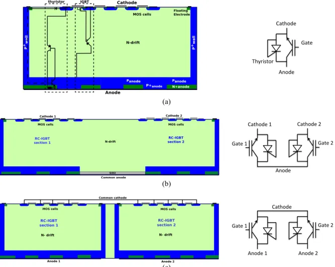
In the domain of power electronics a great importance is given to power systems integration. The integration allows to optimize their compactness and fabrication cost, to improve reliability and performance. In the classical multi-phase power converter (Fig. 1), a great number of silicon power chips, proportional to the number of phase legs, are used. The wire bonds that interconnect all the power chips give rise to stray inductances that impact the reliability and performance of the converter. The monolithic integration of several devices in the same silicon chip allows to reduce the number of power chips to be mounted on the DBC/IMS substrate as well as the number of wire bonds [3-5]. To that end, the two-chip integration approach has been proposed. The goal of this approach is the monolithic integration of the multi-phase power converter within two generic macro-chips [6-7]. The basic structure used for this approach is the RC-IGBT [8-16]. Recently, a study of the two-chip
approach was proposed with the elementary structure being the RC-IGBT-thyristor [1]. This structure integrates monolithically an IGBT and a thyristor in anti-parallel.
In the conventional RC-IGBT, the presence of two diffusions P+anode and N+anode on the backside has an
impact on the I(V) characteristics of the RC-IGBT. Indeed, in forward bias, the N+anode region provides
a path for electrons and thus the device operates as a VDMOS (unipolar) before the IGBT mode (bipolar). The transition from VDMOS mode to IGBT mode is reflected by a snapback in the forward conduction I-V characteristics [17-22]. The non-uniformity of current distribution in the volume of silicon also leads to localized heating and thus limiting the use of the device in terms of current capability and can degrade its reliability [23-25]. Several research works were reported in order to suppress this snapback phenomenon [17-22].
(b)
(a) (c)
Fig. 1: (a) Multi-switch two-chip based integration approach. Cross-sectional view of two three-pole structures that use conventional RC-IGBTs: (b) common anode three-pole chip and (c) common cathode three-pole chip [6-7].
In this paper, we present the RC-IGBT-Thyristor structure as well as the common anode and common cathode power chips that integrate monolithically RC-IGBT-Thyristor structures. Afterwards, a study based on 2D simulations is carried-out in order to highlight the impact of backside dielectrically filled trenches on the electrical characteristics of the RC-IGBT-Thyristor. Then, this RC-IGBT-thyristor is used to create the monolithic multi-pole power chips that are simulated in an inverter mode.
Description of the RC-IGBT-thyristor structure and the monolithic
multi-pole power chips
The cross-sectional view of the RC-IGBT-thyristor is given in figure 2a [1]. The RC-IGBT-thyristor integrates monolithically an IGBT and an anti-parallel thyristor. On the backside, we can see P/P+ diffusions for IGBT mode. By inserting N+ diffusions on the backside of the chip (in P region), we
realize the thyristor sections that ensure reverse conduction. One thyristor section is formed by a succession of four regions Pcathode/N-drift/Panode/N+anode. P+ walls are used for the purpose of thyristor
sections triggering. The backside of the chip is composed of an alternation of N+
anode region and P+anode
region. Figure 2b and 2c show the common anode chip and the common cathode chip, respectively [1]. Each macro-chip is composed of two RC-IGBT-thyristor structures. In the case of the common cathode chip, additional P+ walls are necessary for insulation between the two RC-IGBT-thyristor sections that compose the common cathode three-pole chip.
IGBT1 IGBT3 IGBT2 IGBT4 VHV Common Anode chip Common Cathode chip DC+ DC- Load CHV R drift Short-‐anode Short-‐anode 300µm 1,25 mm 0,54mm 5,6mm 2mm Anode P+ N+ N+ P+ P-‐ P-‐ n cellules P+ P N+ P-‐ ( JTE) Oxyde N-‐ Oxyde
IGBT 1 ( grille 1, cathode 1 ) IGBT 2 ( grille 2, cathode 2 )
N-‐ PN+ N+P P+ P+ Grille2 Cathode2 Anode N+ P+ P-‐ P-‐ PN+ N+P P+ P+ Grille1 Cathode1 N+ P+ P-‐ P-‐ RC-‐IGBT1 RC-‐IGBT2 Cathode1 Cathode2 Anode Short-‐anode P+ N+ N+ P+ P + P-‐ P-‐ P-‐
IGBT 1 ( grille 1, cathode ) IGBT 2 ( grille 2, cathode )
Anode 1 Anode 2 P-‐ P-‐ P-‐ Oxyde P N+ P-‐ ( JTE) Oxyde P+ N-‐ M ur d ’is o la ti o n P+ 300µm 0,54mm 1,25mm 5,6mm 2mm n cellules Short-‐anode N-‐ PN+ N+P P+ P+ Grille2 Cathode Anode1 N+ P+ P-‐ P-‐ PN+ N+P P+ P+ Grille1 N+ P+ P-‐ P-‐ RC-‐IGBT1 RC-‐IGBT2 P-‐ P-‐ P-‐ P-‐ Anode2 P+ Anode2 Anode1 Cathode
(a)
(b)
(c)
Fig. 2: (a) Cross sectional view of the structures and their associated symbol: (a) RC-IGBT-thyristor structure, (b) the common anode chip and (c) the common cathode chip.
2D simulations of the RC-IGBT-thyristor structure (with and without
trenches on the backside)
Static properties: forward and reverse conducting modes
In this study, all 2D numerical simulations are carried-out under SentaurusTM TCAD simulation tool in
quasi-stationary mode. The simulated structures have a thickness of 130 µm and a doping of 1014 cm-3.
The ambient temperature is set at 300 K. The active area of each RC-IGBT chip is of 1 cm2.
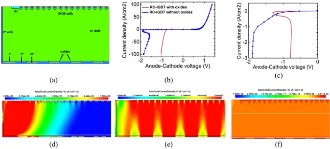
To further facilitate the thyristor triggering, trenches filled with a dielectric (oxide in this case) have been placed around N+
anode regions on the backside. These trenches increase the resistance of the Panode
region and facilitate forward biasing the Panode/N+anode junctions[2].
First of all we have analyzed the impact of oxide trenches on the thyristor turn-on for reverse conducting mode. We have simulated two identical RC-IGBT-thyristor structures, one with and another without dielectric trenches. Figure 3a shows RC-IGBT-thyristor simulated with backside oxide trenches. P+ and N+ diffusions placed on the backside have an equal length of 100 µm.
Figure 3b shows I-V characteristics corresponding to these two structures. For the forward conducting mode, we can notice the snapback phenomenon is suppressed for both RC-IGBT-thyristor structures. Concerning reverse conducting mode, we can see that dielectric trenches on the backside have strongly influenced the thyristor triggering. Indeed, as compared to the initial structure without dielectric trenches, the structure with dielectric trenches turns-on at much lower anode current density
Gate% Anode% Cathode% Thyristor% Gate%2% Cathode%2% Gate%1% Anode% Cathode%1% Gate%2% Gate%1% Anode%1% Cathode% Anode%2%
and presents a voltage drop of about -1V at a current density of -100 A/cm2.
Figure 3d and 3e show current density distribution in reverse conduction (thyristor mode) for RC-IGBT-thyristor with dielectric trenches and without dielectric trenches, respectively. For the structure with dielectric trenches, one can easily notice that all thyristor sections are triggered and the turn-on spreads to the whole structure. While for the structure without dielectric trenches, we can see that only the pilot thyristor is turned-on and the other parallel thyristor sections are not yet triggered. Indeed, N+ diffusions are not sufficiently long enough to allow the turn-on of parallel thyristor sections at this anode current density level.
To see the impact of the P+ wall on the thyristor triggering, RC-IGBT-thyristor (Fig. 3d) has been simulated without P+ wall as shown in figure 3f. The structure is in OFF-state and the thyristor sections did not trigger.
(a) (b) (c)
(d) (e) (f)
Fig. 3: (a) Cross-sectional view of the RC-IGBT-thyristor structure simulated with dielectric trenches on the backside, (b) IA(VAK) characteristics of simulated structures (RC-IGBT-thyristor with dielectric trenches and
without dielectric trenches) and (c) zoom on reverse conducting mode.
Distribution of reverse current density (thyristor mode) at Ianode=-100A/cm2 of RC-IGBT-thyristor structures:
(d) with P+ wall (one thyristor section is triggered), (e) with P+ wall and dielectric trenches (all the thyristor sections are triggered), (f) without P+ wall and without dielectric trenches (thyristor sections are not triggered).
The results presented above showed that dielectric trenches facilitate thyristor turn-on for reverse conduction. In this section, we focus on the influence of the distribution of N+anode and P+anode
diffusions on the distribution of current density and I-V characteristics. In other words, the influence of the number of parallel thyristor sections (for the simulated RC-IGBT-thyristor width) on the static performance of the RC-IGBT-thyristor.
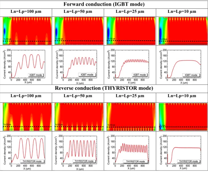
Table I shows the distribution of current density and a curve representing the current density according to a cut line at Y=110 µm (dashed line), for different lengths of N+anode (Ln) and P+anode (Lp). Simulated
structures have a total width of 980 µm and an active area of 1 cm2. For each simulation, the lengths
Ln and Lp are set to be equal.
According to the results, we can notice that the best distribution of current density, for forward and reverse conductions, is obtained for the case of a structure consisting of the great number of alternation of N+
anode and P+anode, i.e. Ln = Lp = 10 µm.
P+#wall#
JTE# MOS#cells#
N1#dri5#
Table I. Influence of the repartitioning of N+anode and P+anode diffusions on the distribution of current density in forward conduction and reverse conduction
Forward conduction (IGBT mode)
Ln=Lp=100 µm Ln=Lp=50 µm Ln=Lp=25 µm Ln=Lp=10 µm
Reverse conduction (THYRISTOR mode)
Ln=Lp=100 µm Ln=Lp=50 µm Ln=Lp=25 µm Ln=Lp=10 µm
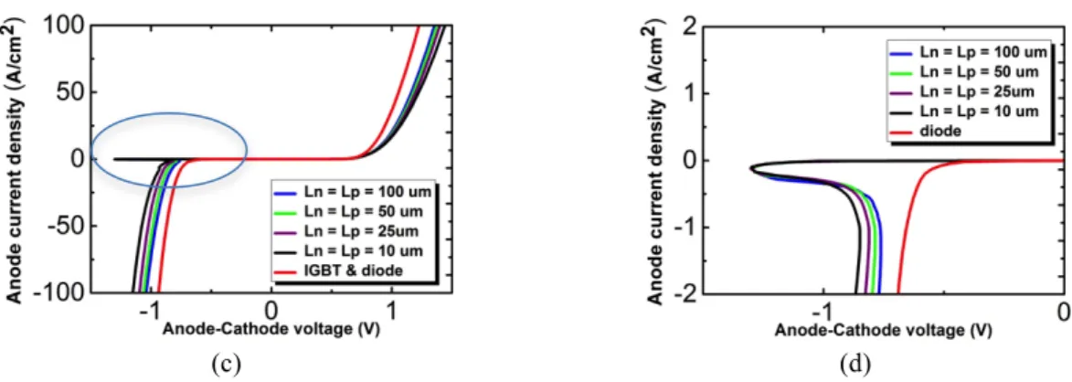
For comparison purposes with the case of RC-IGBT-thyristor structure, we have simulated the IGBT given in figure 4a, and also a PIN diode. These structures have an active area of 1 cm2. IGBT has been
obtained by removing N+ diffusions on the backside of RC-IGBT-thyristor, and the PIN diode has been obtained by removing P/P+ regions on the backside of RC-IGBT-thyristor.
Figure 4a shows the distribution of the current density in IGBT. Figure 4b compares current density distribution within the RC-IGBT-thyristor structures with that within the classical IGBT for forward conducting mode. Figure 4c and 4d show the I-V characteristics corresponding to these simulated structures. One can notice that the classical IGBT and RC-IGBT-thyristor with Ln = Lp = 10 µm have similar performances (current density and I-V characteristics) and therefore, integration of thyristor in IGBT has a weak influence on the IGBT mode and the thyristor mode.
(c) (d)
Fig. 4: (a) Distribution of current density for classical IGBT structure at Ianode=100 A/cm2, (b) curve of current
density in forward conduction (IGBT mode) for RC-IGBT-thyristor structures compared to the classical IGBT structure (cut-line at Y = 100 µm), (c) IA(VAK) characteristics of RC-IGBT-thyristor structures compared to
IGBT and diode, (d) zoom on thyristors turn-on.
Dynamic properties: turn-off for the case of IGBT mode and thyristor mode
We have simulated the RC-IGBT-thyristor in a chopper circuit (Fig. 5a). Figure 5b and 5c show the turn-off waveforms of thyristor and IGBT, respectively. As the results show, an increase of the number of thyristor sections (Ln = Lp = 10 µm) allows to reduce the turn-off time of both IGBT mode and thyristor mode.
(a) (b) (c)
Fig. 5: (a) Simulated electrical circuit, (b) turn-off waveforms of the thyristors (in reverse conducting mode), (c) turn-off waveforms of the IGBTs. Conditions : Ve=600V, I=100A, Vg (RC-IGBT 2)=0/+15V.
Impact of the P+ wall on the thyristor turn-on (case of the RC-IGBT-thyristor with
trenches filled by dielectric on the backside)
A P+ wall is used for the thyristor turn-on in reverse conducting mode of the RC-IGBT-Thyristor structure (see Fig. 3f). Then, we have seen that the use of trenches filled with dielectric on the backside allows improving the thyristor sections triggering and current uniformity. Afterwards, an RC-IGBT-thyristor, with trenches filled with dielectric on the backside, but without P+ wall, for Ln=10 µm and Ln=100 µm were simulated (quasi-stationary 2D simulations). From the obtained results, one can notice that all thyristor sections are triggered (Fig. 6).
(a) (b)
Fig. 6: Reverse conducting mode (thyristor mode) of the RC-IGBT-thyristor without P+ wall: (a) structure with Ln=Lp=100 µm and (b) structure with Ln=Lp=10 µm.
RC-IGBT1 RC-IGBT2 VHV DC+ DC- CHV I=100A& VGS& A& K& A& K& G& G&
2D simulations of the multi-pole chips: “two-chip” H-bridge converter
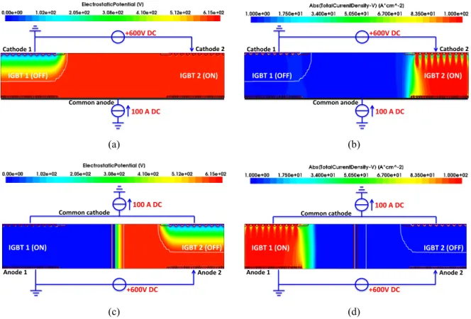
The two chips have been first simulated separately as shown in figure 7. Then, the two macro-chips were associated to form a complete H-bridge and simulated in the inverter configuration. For comparison purposes, we have also simulated a conventional H-bridge made of four discrete RC-IGBTs. It should be noted that for the multi-pole chips the P+ walls were suppressed. There is only a P+ wall for insulation between the RC-IGBT-thyristor sections of the same common cathode chip. Figure 8 shows output characteristics of the two-chip H-bridge and the conventional H-bridge in inverter modes.(a) (b)
(c) (d)
Fig. 7: Common anode chip: (a) equipotential lines in the OFF-state RC-IGBT (left section) and (b) distribution of current density in the ON-state RC-IGBT (right section). Common cathode chip: (c) equipotential lines in the OFF-state RC-IGBT (right section) and (d) distribution of current density in the ON-state RC-IGBT (left section).
(a) (b)
Fig. 8: Output characteristics of the inverters: (a) the two-chip H-bridge configuration, (b) the conventional H-bridge. +600V%DC% 100%A%DC% IGBT%2%(ON)% IGBT%1%(OFF)% Cathode%1% Cathode%2% Common%anode% +600V%DC% 100%A%DC% IGBT%2%(ON)% IGBT%1%(OFF)% Cathode%1% Cathode%2% Common%anode% +600V%DC% IGBT%2%(OFF)% IGBT%1%(ON)% Anode%1% Anode%2% 100%A%DC% Common%cathode% +600V%DC% 100%A%DC% IGBT%2%(OFF)% IGBT%1%(ON)% Anode%1% Anode%2% Common%cathode%
Conclusion
An RC-IGBT-thyristor that uses trenches filled with dielectric on the backside has been studied and analyzed by SentaurusTM TCAD simulations. The use of trenches filled with dielectric facilitates the
thyristor triggering in reverse conduction. We have also noticed that reducing N+ diffusions length
(and P diffusion length) allows to reach a more uniform current density distribution for both forward and reverse conductions. In dynamic, the reduction of Ln length allows to reduce the turn-off time for both IGBT mode and thyristor mode. In summary, a reduction of Ln length, which corresponds to an increase of the number of thyristor in parallel, allowed to improve both static and dynamic performances of RC-IGBT-thyristor. In the context of power integration, RC-IGBT-thyristor with trenches filled with dielectric was used to realize the monolithic multi-pole chips. These chips were simulated separately and then associated to form an H-bridge inverter. For comparison purposes, a conventional H-bridge converter and an H-bridge converter based on the two-chip approach were simulated.
References
[1] A. Lale, A. Bourennane, A. El khadiry, F. Richardeau, "A generic Reverse Conducting IGBT structure for monolithic switching cells integration," Power Electronics and Applications (EPE'14-ECCE Europe), 2014 16th European Conference on, vol., no., pp.1-10, 26-28 Aug. 2014.
[2] Liheng Zhu; Xingbi Chen, "A novel snapback-free reverse conducting IGBT with anti-parallel Shockley diode," Power Semiconductor Devices and ICs (ISPSD), 2013 25th International Symposium on, vol., no., pp.261, 264, 26-30 May 2013.
[3] D. Reusch, J. Strydom, A. Lidow, "Monolithic integration of GaN Transistors for Higher Efficiency and Power Density in DC-DC Converters", PCIM Europe 2015, Nuremberg, Germany.
[4] Hara, K.; Wada, S.; Sakano, J.; Oda, T.; Sakurai, K.; Yamashita, H.; Utsumi, T., "600V single chip inverter IC with new SOI technology," Power Semiconductor Devices & IC's (ISPSD), 2014 IEEE 26th International
Symposium on, vol., no., pp.418,421, 15-19 June 2014.
[5] D.W Green, E.M Shankar Narayanan, "Fully Isolated High Side and Low Side LIGBTs in Junction Isolation Technology", Power Semiconductor Devices and IC's, ISPSD 2006. IEEE International Symposium on, pp.1-4, 2006.
[6] A. Bourennane, M.Breil-Dupuy, F.Richardeau and J-L. Sanchez. Patent number: 11/59137, Date: Oct. 10 - 2011, by: Centre National de la Recherche Scientifique (CNRS), Institut National Polytechnique de Toulouse. Title: "Cellule monolithique de circuit intégré et notamment cellule de commutation monolithique".
[7] A. El Khadiry, A. Bourennane, M. Breil and F. Richardeau, "Monolithically integrated switching cells suitable for high density power conversion", (ISPS’12), Prague, pp. 222-227.
[8] K. Takahashi et al., "1200V Class Reverse Conducting IGBT optimized for Hard Switching Inverter", PCIM Europe 2014, Nuremberg, Germany.
[9] L. Storasta et al., "Resolving Design Trade-offs with the BIGT Concept", PCIM Europe 2014, Nuremberg, Germany.
[10] Jongil Won et al., "Reverse conducting IGBT using MEMS technology on the wafer technology", ETRI journal, Volume 35, Number 4, 2013.
[11] J. Won et al., "Reverse-Conducting IGBT using MEMS technology on the wafer back side", ETRI journal, Volume 35, Number 4, August 2013.
[12] H. Jiang et al., "Low turn-off loss reverse conducting IGBT with double n-p-n electron extraction paths", the institution of engineering and technology, 2012.
[13] T. Kimmer, J. Oehmen, P. Türkes, S. Voss, "Reverse Conducting IGBT—A new Technology to Increase the Energy Efficiency of Induction Cookers", PESC 2008, pp.2284-2287.
[14] Z. Wenliang et al., "The negative differential resistance characteristics of an RC-IGBT and its equivalent circuit model", Journal of Semiconductors, vol. 35, No. 2, February 2014.
[15] Weizhong Chen et al., "A high reliable reverse-conducting IGBT with a floating P-plug," Power Semiconductor Devices and ICs (ISPSD), 2013 25th International Symposium on , vol., no., pp.265-268, 26-30 May 2013.
[16] Jae Hong Park, Methods of forming insulated gate bipolar transistors having built-in freewheeling diodes and transistors formed thereby, U.S. Pat. No. 5, 702, 961.
[17] W. Chen et al., "A snapback suppressed reverse-conducting IGBT with soft reverse recovery characteristic", Superlattices and Microstructures 61 (2013) 59–68.
[18] M. Antoniou et al., "A new way to alleviate the RC IGBT snapback phenomenon: The Super Junction solution," Power Semiconductor Devices & IC's (ISPSD), 2010 22nd International Symposium on , vol., no., pp.153-156, 6-10 June 2010.
[19] Huaping Jiang et al., "A Snapback Suppressed Reverse Conducting IGBT with Oxide Trench Collector," Power and Energy Engineering Conference (APPEEC), 2012 Asia-Pacific, vol., no., pp.1-4, 27-29 March 2012. [20] Huaping Jiang et al., "A Snapback Suppressed Reverse-Conducting IGBT With a Floating p-Region in Trench Collector", Electron Device Letters, IEEE, vol. 33, no. 3, pp.417-419, 2012.
[21] A. Bourennane, F. Mura, J-L. Sanchez, F. Richardeau, M. Breil, P. Austin, "Structure bidirectionnelle en courant", Revue internationale de génie électrique, pp. 553-565, RS-RIGE-10/2007.
[22] H. Ruthing et al., "600 V Reverse Conducting (RC-) IGBT for Drives Applications in Ultra-Thin Wafer Technology", Power Semiconductor Devices and IC's, ISPSD '07. 19th International Symposium on, pp.89-92, 2007.
[23] C. Wein-Zhong et al., "A snapback suppressed reverse-conducting IGBT with uniform temperature distribution" Chin. Phys. B, vol. 23, No. 1, 2014.
[24] Liheng Zhu, Xingbi Chen, "An Investigation of a Novel Snapback-Free Reverse-Conducting IGBT and With Dual Gates" Electron Devices, IEEE Transactions on , vol.59, no.11, pp.3048-3053, Nov. 2012.
[25] D. Wigger, H-G Eckel, "Influence of the charge distribution on the electrical behavior of the BIGT", PCIM Europe 2014, Nuremberg, Germany.