HAL Id: hal-01373042
https://hal.archives-ouvertes.fr/hal-01373042
Submitted on 28 Sep 2016
HAL is a multi-disciplinary open access
archive for the deposit and dissemination of
sci-entific research documents, whether they are
pub-lished or not. The documents may come from
teaching and research institutions in France or
abroad, or from public or private research centers.
L’archive ouverte pluridisciplinaire HAL, est
destinée au dépôt et à la diffusion de documents
scientifiques de niveau recherche, publiés ou non,
émanant des établissements d’enseignement et de
recherche français ou étrangers, des laboratoires
publics ou privés.
Comparison of topside contact layouts for power dies
embedded in PCB
Chenjiang Yu, Cyril Buttay, Eric Labouré, Vincent Bley, Céline Combettes,
Gilles Brillat
To cite this version:
Chenjiang Yu, Cyril Buttay, Eric Labouré, Vincent Bley, Céline Combettes, et al.. Comparison of
topside contact layouts for power dies embedded in PCB. ESTC, IMAPS, Sep 2016, Grenoble, France.
�10.1109/ESTC.2016.7764707�. �hal-01373042�
Comparison of topside contact layouts for power dies embedded in PCB
Chenjiang Y
U1, Cyril B
UTTAY2, ´
Eric L
ABOURE´
1, Vincent B
LEY3,
C´eline C
OMBETTES3, Gilles B
RILLAT3GeePs, UMR CNRS 8507, CentraleSup´elec, Univ. Paris-Sud
Universit´e Paris-Saclay Sorbonne Universit´es UPMC Univ Paris 06, 3 & 11 rue
Joliot-Curie Plateau de Moulon 91192 Gif-sur-Yvette CEDEX, France
Laboratoire Amp`ere CNRS UMR 5005, Bat L de Vinci, 21 av. Capelle, 69621 Villeurbanne,
France,
cyril.buttay@insa-lyon.fr
Universit´e de Toulouse; UPS, INPT; LAPLACE;
118 route de Narbonne - Bˆat. 3R3 F-31062 Toulouse cedex 9, France.
CNRS; LAPLACE; F-31062 Toulouse, France
Abstract
Embedding of power semiconductor dies in PCB is a very attractive technology, especially to achieve interconnects with a very low parasitic inductance and resistance. In this paper, we focus on the contact resistance and current distri-bution in a large (6×6mm2) diode embedded in PCB, as a function of the layout of its topside contact. We demonstrate that by choosing a suitable contact layout, it is possible to achieve a very low contact resistance.
Introduction
Large wide bandgap power semiconductors (especially those based on silicon carbide or gallium nitride) bring very high switching speed capability, which can reach several kiloamperes per microsecond, and voltages of more than 10 kilovolts per microsecond. These devices make it possible to reduce the size of converters or to increase the conversion efficiency. However, as the conventional electrical inter-connections are usually established by wire-bonding, which has large stray inductances, the high frequency switching generates high switching losses. To avoid this drawback and take full advantage of these fast components, it is nec-essary to design very low inductance interconnects. For example, in [1], the authors present a switching cell with a sub-nanohenry inductance designed for GaN transistors. For such high-density and low inductance interconnects, the printed-circuit board (PCB) technology is very attractive. This technology offers a variety of interconnect possibili-ties, and make it possible to process many dies at once. Among the various proposed PCB solutions, we will focus on those that make use of rigid PCB technology, with boards thicknesses ranging from a few hundred of microns up to a few millimetres. Thanks to this thickness, devices can be embedded within the PCB substrate. For example, various manufacturers sell dielectric layers that can be introduced in the stack of a multilayer PCB to form capacitors [2]. An example of a converter integrating such capacitive layers is given in [3]. In the same paper, the authors also stack some magnetic layers to form an ”Embedded Passive Integrated Circuit” (emPIC).
One weak point of PCBs technology is its poor thermal conductivity (usually lower than 1 W/mK, as compared to 24 W/mK for alumina or 150 W/mK for AlN ceram-ics), while power semiconductor devices produce usually a high power density(100 W/cm2). For this reason, many
re-searchers focus on integrating the active rather than the pas-sive devices in the PCB. This allows for a shorter distance between the active component and the cooling system [4]. In [5], the authors describe some commercially-available PCB integration technologies for active devices. Many of these technologies were developed through the European projects ”Hermes” and ”Hiding Dies”, or through the Ger-man project ”HiLevel”. These projects included work on the manufacturing technology, on the design tools, and on validation [6]. In particular, one of the demonstrators of the ”HiLevel” project included a 50 kW inverter for hybrid cars, which is described in [7]: the dies are firstly soldered to a thick copper layer (for thermal management), and then em-bedded in PCB layers. The pads of the dies are then exposed by removing the insulating material with a laser. In [8], the exposition of the pads is performed by mechanically grind-ing away the PCB materials. This results a converter of very low parasitic inductances, and allows for very close decou-pling, as the decoupling capacitors are mounted directly on top of the power semiconductor dies.
Some authors do not use the PCB material, but the struc-tures they propose offer many feastruc-tures of PCB embedding. For example, in [9], power die are attached on a DBC and integrated in a ceramic frame. In [10], a polyimide layer is employed around the dies. Finally, the ¨SiPLIT¨ [11] tech-nology, uses some steps of the PCB technology (lamination, electroplating) to form a power module with very low para-sitic inductances.
In this paper, we give firstly a short presentation of the em-bedding technology process we use. Then, test vehicles dedicated to the study of the contact resistance are pre-sented. Following this, we propose an electrical model for these test vehicles, and we compare the calculations and ex-perimentation results of these vehicles.
(a) (b) (c) (d) (e) (f)
Figure 1: The different stages of the die embedding process: a die is silver-sintered onto a substrate (a), then prepregs and copper foil are stacked (b). This stack is laminated (c). The copper foil is chemically etched above the die (d), and the exposed epoxy material is ablated using a CO2laser (e).
Finally, electroplated copper is deposited to connect the die topside (f).
Embedding technology
The embedding process is detailed in [12], and summarized in figure 1. It is performed in-house using prototype-scale equipment.
First, the dies are prepared: most dies currently available on the market have an aluminium topside finish, which is not compatible with our embedding technology [12]. A copper layer must therefore be deposited prior to the embedding. This is performed by evaporating a titanium adhesion layer (50 nm), followed by copper (150 nm or 500 nm) through a shadow mask in a PVD system (electron beam system EVA300, Alliance concept).
The workflow for embedding is as follows:
a The die to be embedded is attached to a copper or DBC substrate using silver sintering. With solder, the die would float on a liquid layer during reflow, and could move slightly. With silver-sintering, which is a solid-state technology, the die remains exactly at the same position throughout the process. This is important as the die is no longer visible once embedded. Silver sin-tering is performed without pressure (in an oven), us-ing material from Heræus (Microbond ASP295-series) b The outline of the die is laser-cut in layers of prepreg (FR4 Isola 370HR), which are stacked on the substrate (alignment holes are also present on the prepreg layer and the substrate, to register with alignment pins in the pressing system). Some more prepreg layers are stacked on top of the die (Arlon 55NT, epoxy material with a non woven aramid substrate, is used instead of FR4 because it leaves fewer residues after the laser ab-lation that comes later in the process). A 35 µm-thick copper foil is placed on top of the stack
c The stack is then laminated, in a hot press (90 minutes, 195 °C, 13 bars).
d A window is etched in the copper above the die. This is performed using standard PCB photolithography (the PCB is laminated with dry-film photoresist, exposed through a mask, developped, and then etched using fer-ric chloride). This step requires careful alignment with the die, which is no longer visible (hence the need for silver sintering in step (a)). The registering of the mask is performed using the alignment holes used in step (b). e The fiber-resin composite which is exposed through the window in the copper is ablated using a CO2laser
(Gravograph LS100EX 60 watt, 10.6 µm wavelength).
(a)
(b)
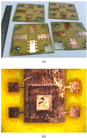
Figure 2: Left: some of the test vehicles, with 4 embedded diodes each. Each test vehicle is approximately 60×60 mm2. Right: close-up of one of
the embedded dies, with a contact window of 3×3 mm2. The die size is 6×6 mm2.
As copper is not affected by the laser, this step is fairly robust: the alignment is provided by the window in the topside copper foil, and the ablation stops as soon as the laser hits the copper metallization of the die. Therefore, there is no need for a very accurate control of the laser parameters.
f Finally, a new coat of copper is applied by electroplat-ing (standard “metallized holes” PCB process, uselectroplat-ing chemistry from Bungard Electronik).
After these steps, the resulting PCB can be processed in a standard way (photosensitive material coating, exposure, development, copper etching) to pattern its top copper layer. Test Vehicles
Special test vehicles were designed and manufactured for this study (figure 2): They consist in 600 V, 6×6 mm2 dies (Microsemi, packaged part reference APT60D60BG)
Die
Topside copper
Wells
R
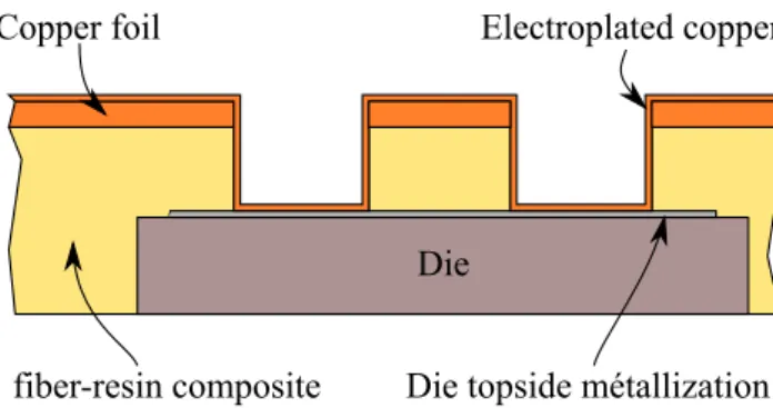
Figure 3: 3D view of the test vehicles (fiber-resin composite not shown): a die (diode) is connected through a number of wells (here 4) to the top copper layer of a PCB. The number of wells and their size is varied.
Copper foil
Electroplated copper
Die
Die topside métallization
fiber-resin composite
Figure 4: Cross-section of the test vehicle from Fig. 3.
embedded in PCB with various contact layouts (from 1 to 16 mm2, in 1 to 9 areas). The layout of the test vehicles is designed to allow for 4-point measurements.
Fig. 3 presents a 3-D view of the test vehicle (the fiber-resin composite which encapsulates the die is not shown for better clarity). Here, 4 openings were made in the topside copper layer, resulting in 4 contact “wells” with the die. A cross section (Fig. 4) shows that the copper layer is thicker on top (because it is formed by a 35 µm copper foil, on top of which some more copper is electroplated). The walls and floor of the wells is only formed by the electroplated copper and is therefore thinner (7 µm here, but this can be adjusted by changing the duration of the electroplating step). As a consequence, the layout of the wells is expected to have an influence on the resistance of the interconnects: small well area leaves more (thick) topside copper, but of-fers smaller contact area with the die. A single well can maximize the contact area with the die, but removes a large part of the topside copper, and only has limited wall surface on the wells. A small, single well will result in a poor cur-rent distribution on the die surface [13]. This trade-off is explored in this paper.
For practical reasons, not all the configurations can be made. In particular, we fixed a minimum well dimension of 1x1 mm2, and left a 1 mm margin on the edge of the diode (we consider a 4x4 mm2useable area out of a 6x6 mm2die).
# of Surface Resistance Image
contacts (mm2) (mΩ) in Fig. 6 1 1 3.80 (a) 1 4 2.16 (b) 1 9 1.55 (c) 1 16 1.32 (d) 4 4 1.40 (e) 4 9 1.26 (f) 9 9 1.13 (g)
Table 1: Contact resistance for the different layouts presented in figure 6.
Rtop Rwall Rcont Rdie RAl Raccess Vin
Figure 5: 2-D view of the resistance network used to represent the test vehicles
Table 1 lists the configurations investigated: 4 die contact areas (1, 4, 9 and 16 mm2) and 1, 4 or 9 wells.
Modelling
The calculation of the contact resistance is performed using a Python script [14]. the conductors in the structure are di-vided in 100×100 µm elements in which unidirectional cur-rent flow is assumed. These elements are connected to form an equivalent resistance network, and calculations based on the modified nodal analysis1 are performed to simulate the
current distribution.
A 2-D circuit diagram is presented in Fig. 5. It shows the various resistances considered in the calculations:
• Rtopis the resistance of the top copper layer, whose
thickness is that of the initial copper foil (35 µm), plus the electroplated copper layer (7 µm);
• Rwall is the resistance of the “walls” and the “floor”
of the wells. Here, the thickness considered is that of the electroplated copper only, and the well are 400 µm-deep;
• RAl is the resistance of the aluminium topside metal
layer (3 µm thick) of the die (the thin PVD Ti/Cu layers are considered negligible);
• Rdie is the equivalent resistance of the die. We
con-sider the silicon to be uniformly doped at 10−19cm−3, corresponding to a resistivity of 6.10−5Ωm, with a die 1http://www.swarthmore.edu/NatSci/echeeve1/Ref/
# of Surface Resistance Min Max contacts (mm2) (mΩ) (mΩ) (mΩ) 1 1 16.5 13.6 19.15 1 4 5.64 4.66 6.62 1 9 4.85 4.26 5.43 1 16 4.65 4.48 4.83 4 4 5.38 4.49 5.72 4 9 4.38 4.14 4.55 9 9 5.18 4.27 5.80
Table 2: Resistance measurements. 2 test vehicles were used for the “sin-gle contact” cases (top 4 lines), 3 tests vehicles were used for the remaining lines.
thickness of 400 µm. This is a very coarse assumption, which causes probably most of the mismatch between the resistance values in simulation and experiment; • Raccess is a resistance added between the voltage
source and the nodes on one of the edges of the top copper layer. Its value is chosen equal to Rtop;
• Rcontis the contact resistance between the copper
lay-ers and the die. By default, it is considered negligi-ble (1 nΩ).
In each of the layer, the resistance of each element is simply calculated as
R = ρl
dw, (1)
with ρ the resistivity of the material (16.78 nΩm for copper, 28.2 nΩm for aluminium, 65 µΩm for silicon), l the length of an element, d its thickness, and w its width.
The results of the calculations for the various configurations of the test vehicles are presented in fig. 6, and the corre-sponding resistance values are given in table 1.
Results
Experimental characterization of the test vehicles was per-formed using a Tektronix 371A Curve tracer, using 4-point connections and pulsed mode, with maximum current of 100 A. As an example, the measurements obtained for two of the test vehicles are given in figure 7. From these measurements, we identified the dynamic resistance of the diode. As a comparison, earlier studies found that a pack-aged (TO247) version of the diode has a dynamic resistance of 4.4 mΩ (considering a 100 A current range, as in this pa-per) [15].
The resistance values obtained experimentally are presented in table 2. They are much higher than the calculated ones (table 1): between 16.5 mΩ and 4.38 mΩ experimentally, versus 3.8 mΩ–1.13 mΩ in simulation. This can be due to several factors: many parameters of the simulation are based on assumptions, and in particular the equivalent restance of the diode itself is probably not correct. Another is-sue might be the contact resistance between the aluminium topside metal of the diode and the electroplated copper (dis-cussed below).
However, even with this large difference between experi-ments and calculation, some conclusions can be drawn:
• The surface plots in fig. 6 show that when a single well is used, most of the voltage drop occurs on the topside metal of the die. This is especially true for 1 mm2 wells (fig. 6a). As the well grows, the resis-tance drops 4 times in measurements (from 16.5 mΩ at 1 mm2down to 4.65 mΩ at 16 mm2, table 2) and 3 times in simulation (from 3.8 mΩ to 1.32 mΩ, table 1). • Multiple contacts allow for a better current spreading over the die metallization, even with smaller contact area: in table 1, 4 and 9- contact versions (the last three lines of the table) offer resistance of 1.4 to 1.13 mΩ , comparable to that of a single well with 16 mm2area,
with a fourth to a half of the surface (4 or 9 mm2).
Similar results can be observed from the experiments in table 2, although with more variation.
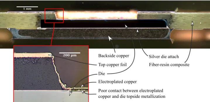
• The poor contact between the electroplated layer and the die topside metallization, visible in the close-up view in fig. 9 is probably responsible for a large part of the difference between the simulations and the mea-surements. Running the simulations with a much higher contact resistance value (1 Ω instead of 1 nΩ for a 100×100 µm2element) results in calculated val-ues much closer to the measurements (between 2.3 and 17 mΩ).
• In theory, it is possible to achieve contact resis-tances much lower than those obtained with wirebonds (4.4 mΩ). The best measurements described in table 2 are already better than regular wirebonded devices, de-spite the poor copper/die interface.
Investigations shows that the poor quality of the electro-plated/die interface seems to be caused by the plating pro-cess: after the laser ablation (fig 1e), the exposed surface of the die retains a copper color (Ti/Cu PVD layers were applied to the dies prior to embedding). The plating pro-cess, however, uses a series of baths, some of which hav-ing a aggressive action to ensure the surface to be plated are clean. It is probably one of those bath which degrades the PVD layers and causes poor adhesion between the die and the electroplated copper. Increasing the thickness of the PVD copper layer from 150 nm to 500 nm helped reduce the resistance from 9.89 mΩ for a 4 mm2contact down to
5.64 mΩ (all the results presented in this article are with 500 nm PVD copper layer).
Conclusion
Embedding power dies in PCB is an attractive solution, be-cause it allows for more compact circuits, with lower stray inductances. The results presented in this article show that it is also possible to achieve very low interconnect resistances, providing the contacts with the topside metallization of the dies allow for a good spreading of the current.
Experiments demonstrated resistances lower than those of-fered by standard thick-wire aluminium wirebonds, al-though (in our case) improvements are required at the elec-troplated copper/die interface. With a proper interface even lower resistances values should be easily achieved.
(a) (b) (c) (d) (e) (f) (g)
0.0
0.1
0.2
0.3
0.4
0.5
0.6
0.7
0.8
0.9
1.0
Voltage [V]
(h)Figure 6: Simulation of the voltage ditribution on the PCB top copper layer and on the topside metallization of the die, for various contact layout configurations. Current is injected on the left side on the top metallization, and on the backside of the die.
0.8 1.0 1.2 1.4 1.6 1.8 2.0 Voltage [V] 0 20 40 60 80 100 Current [A] 13.60m Ω 6.62 mΩ 5.43 mΩ 4.83 mΩ 1 mm² contact 4 mm² contact 9 mm² contact 16 mm² contact
Figure 7: Forward characteristic measured on test vehicle #7, which com-prises single well layouts with a surface ranging from 1 to 16 mm2 (corre-sponding to Fig. 6a) to Fig. 6d).
0.8 1.0 1.2 1.4 1.6 1.8 2.0 Voltage [V] 0 20 40 60 80 100 Current [A] 19.15m Ω 4.66 mΩ 4.26 mΩ 4.48mΩ 1 mm² contact 4 mm² contact 9 mm² contact 16 mm² contact
Figure 8: Forward characteristic measured on test vehicle #9, with the same layout as test vehicle #7 (Fig. 8). Here, the 9 mm2contact is found to offer a lower resistance than the 16 mm2contact.
Die
Electroplated copper Top copper foil
Backside copper Silver die attach
Poor contact between electroplated copper and die topside metallization
Fiber-resin composite
Figure 9: Cross-section of one of the diodes from test vehicle #9 (9 mm2), with a zoom on the left wall of the contact well. The difference in colors between both pictures is due to a change in microscope illumination (darkfield for the top photograph, brightfield for the enlargement).
References
[1] K. Klein, E. Hoene, and K.-D. Lang, “Packages for Fast Switching HV GaN Power Devices.” in Proceedings of the PCIM 2014 confer-ence, 2014.
[2] J. Andresakis, “Embedded Capacitors,” Oak-Mitsui Technologies, presentation, Nov. 2005. [Online]. Available: http://www.laocsmta. org/archive/Embedded Capacitance Presentation.pdf
[3] E. Waffenschmidt, B. Ackermann, and J. A. Ferreira, “Design Method and Material Technologies for Passives in Printed Circuit Board Embedded Circuits,” IEEE Transactions on Power Electron-ics, vol. 20, no. 3, pp. 576–584, May 2005.
[4] A. Alderman, L. Burgyan, B. Narveson, and E. Parker, “3-D Embed-ded Packaging Technology,” IEEE Power Electronics Magazine, pp. 30–39, dec 2015.
[5] E. Parker and B. Narveson, “Increase Power Density and Performance Using 3D Packaging,” PSMA, Tech. Rep., 2014. [Online]. Available: http://www.apec-conf.org/wp-content/uploads/ 2014/03/IS1-5-1.pdf
[6] M. Brizoux, A. Grivon, W. Maia Filho et al., “Development of a Design & Manufacturing Environment for Reliable and Cost-Effective PCB Embedding Technology,” in IPC Apex Expo conference, 2011. [Online]. Available: https://www.smtnet.com/ library/files/upload/embedded-chips.pdf
[7] A. Ostmann, L. Boettcher, D. Manessis, S. Karaszkiewicz, and K.-D. Lang, “Power modules with embedded components,” in Microelec-tronics Packaging Conference (EMPC) , 2013 European, Sep. 2013, pp. 1–4.
[8] E. Hoene, A. Ostmann, B. T. Lai, C. Markczok, A. M¨using, and J. W. Kolar, “Ultra-Low-Inductance Power Module for Fast Switch-ing Semicon-ductors,” in Proc. PCIM Europe, 2013, pp. 1–8. [9] N. Zhu, S. Lee, J. Van Wyk, W. Odendaal, and Z. Liang, “Thermal
Stress and Intrinsic Residual Stress in Embedded Power Modules,” in Industry Applications Conference, 2003. 38thIAS Annual Meeting.
Conference Record of the, 2003.
[10] P. Ning, T. G. Lei, F. Wang, G.-Q. Lu, K. D. Ngo, and K. Ra-jashekara, “A novel high-temperature planar package for SiC mul-tichip phase-leg power module,” Power Electronics, IEEE Transac-tions on, vol. 25, no. 8, pp. 2059–2067, 2010.
[11] K. Weidner, M. Kaspar, and N. Seliger, “Planar Interconnect Tech-nology for Power Module System Integration,” in Integrated Power
Electronics Systems (CIPS), 2012 7thInternational Conference on.
IEEE, 2012, pp. 1–5.
[12] C. Yu, C. Buttay, E. Labour´e, V. Bley, and C. Combettes, “Highly integrated power electronic converters using active devices embedded in printed-circuit board,” in 4th Micro/Nano-Electronics, packaging and assembling, design and manufacturing forum MiNaPAD 2015. Grenoble, France: IMAPS, Apr. 2015. [Online]. Available: https://hal.archives-ouvertes.fr/hal-01197043
[13] E. Vagnon, Y. Avenas, J.-C. Cr´ebier, P.-O. Jeannin, I. A. Batta, and A. Besri, “Electrical Characterization of a Pressed Contact Between a Power Chip and a Metal Electrode,” in I2MTC 2009, Singapour, Singapour, 2009, p. . [Online]. Available: http://hal.archives-ouvertes.fr/hal-00384063
[14] J. D. Hunter, “Matplotlib: A 2D graphics environment,” Computing In Science & Engineering, vol. 9, no. 3, pp. 90–95, 2007.
[15] B. Mouawad, B. Thollin, C. Buttay, L. Dupont, V. Bley, D. Fabr`egue, M. Soueidan, B. Schlegel, J. Pezard, and J.-C. Crebier, “Direct Copper Bonding for Power Interconnects: Design, Manufacturing and Test,” IEEE transactions on Components, Packaging and Manufacturing Technology, vol. 5, no. 1, pp. 143–150, jan 2015. [Online]. Available: https://hal.archives-ouvertes.fr/hal-01207014


![[PDF] Introduction à XML pas à pas documentation de formation | Cours informatique](data:image/gif;base64,R0lGODlhAQABAIAAAP///wAAACH5BAEAAAAALAAAAAABAAEAAAICRAEAOw==)