M R S
I
nternet
J
ournal o f
N
itride
S
emiconductor
R
esearch
Volume 2, Article 4
Improved optical activation of ion-implanted Zn acceptors in GaN by
annealing under N
2
overpressure
A. Pelzmann
Abteilung Optoelektronik, Universität Ulm S. Strite
IBM Research Division, Zurich Research Laboratory A. Dommann
Neu-Technikum Buchs
C. Kirchner, Markus Kamp , K. J. Ebeling Abteilung Optoelektronik, Universität Ulm
A. Nazzal
IBM Almaden Research Center, 650 Harry Road, San Jose CA 95120-6099 USA
This article was received on December 30, 1996 and accepted on January 24, 1997.
Abstract
We investigated the properties of ion-implanted GaN:Zn annealed under various conditions using photoluminescence (PL) and high resolution x-ray diffraction (HRXRD). Epitaxial GaN/sapphire of high optical quality was ion-implanted with a 1013 cm-2 dose of Zn+ ions at 200 keV. The sample was capped with 200 Å of SiNx and then diced into numerous pieces which were annealed under varied conditions in an attempt to optically activate the Zn. Annealing was performed in a tube furnace under flowing N2, an atmospheric pressure MOCVD reactor under flowing NH3 or N2, and under an N2 overpressure of 190 atm. The observed improvement in the optical quality of GaN:Zn annealed under N2 overpressure yields further insights into the trade-off between defect annealing and N loss from the GaN crystal.
1. Introduction
1.1. Purpose of the Investigation
Ion-implantation is widely used in semiconductor device technology to locally alter the electrical properties of materials, e.g. for doping or isolation. GaN device technology is rapidly advancing towards maturity. For electronic device applications, it is likely that techniques of optimally ion-implanting and activating impurities in GaN will need to be developed.
GaN LEDs can luminescence in any of the visible colors dependent on the dopant introduced [1]. If it is possible to realize good optical quality implanted GaN, LEDs and electronic devices could benefit from dopants incompatible with epitaxial growth processes. It would also be possible to fabricate monolithic multicolor LED arrays [2][3] by selective area implantation of different color centers. Such arrays could be useful for color printing, or as tiny, bright, high information content displays.
Typically ion-implantation introduces damage to the crystal which must be annealed out. This procedure is routine in semiconductors such as Si in which crystal repair occurs at temperatures well below those causing decomposition. In
y p p g p the case of compound semiconductors, rapid thermal annealing (RTA) at temperatures near or above the
decomposition temperature is often preferred, usually in the presence of an overpressure of a stabilizing gas, such as arsenic for GaAs or phosphorus for InP, to limit decomposition.
The situation in GaN is more complex since this material has both strong bonding, and a constituent, N, having high vapor pressure. The strong bonding limits the beneficial effects of annealing on the structural quality of the crystal while the overriding desire of N atoms to be in the gas phase greatly lowers the decomposition temperature of GaN. Thus, techniques must be sought which provide significant crystal repair and good activation of implanted impurities while avoiding N loss to the GaN crystal.
1.2. Background
Two groups in the 1970’s reported PL in ion-implanted GaN. Pankove and Hutchby [4] implanted 35 different elements into GaN, reporting on GaN:Zn in detail [5]. Metcalfe et al. [6] investigated As and P doping. Each found that post-implantation annealing activates the dopants, but no estimates of the absolute PL efficiency were given. Recently, the electrical properties [7][8] and thermal stability [9][10][11] of dopant-implanted GaN have received growing attention, highlighted by the demonstration of implant isolation for electronic devices [12] and the electrical activation of p-type Ca acceptors [13].
Recently, we described [14] the structural and optical properties of ion-implanted GaN:Zn which was annealed at atmospheric pressure under flowing N2 at temperatures as high as 1100 °C for durations ranging from 1 minute (RTA) to 1 hour (tube furnace). These data showed that annealing at or above 1000 °C removes a significant portion of the implantation damage, however at the expense of nitrogen loss from the GaN crystal. Due to this tradeoff, our previously best RTA annealed samples had merely several percent of the room temperature PL efficiency of an epitaxial GaN:Zn sample having a comparable Zn dopant concentration.
1.3. Present Study
With the goal of eliminating N loss from GaN during annealing, we have extended our earlier study to ion-implanted GaN:Zn annealed under NH3 at atmospheric pressure, and N2 at 190 atm. overpressure. Both of these
experimental conditions are designed to inhibit nitrogen loss by increasing the amount of active nitrogen available to stabilize the GaN.
2. Experiment
2.1. Initial Material
The initial sample was a 1.5 µm GaN/AlN/c-sapphire MOVPE-grown epilayer purchased from Cree Research having a background electron concentration of roughly 5 x 1016 cm-3 which exhibited strong bandedge and negligible midgap room temperature PL. The epitaxially doped GaN:Zn PL standard was also purchased from Cree Research which consisted of a 1.9 µm GaN/AlN/c-sapphire structure which was capped by a 0.28 µm GaN:Zn layer having an approximate Zn concentration of 2 x 1018 cm-3. The thickness and Zn concentration of the doped layer was chosen to correspond to the experimentally measured Zn distribution in the ion-implanted samples under study [14].
2.2. Ion-Implantation
A single, room-temperature dose of 1013 cm-2 of 200 keV Zn+ ions were implanted uniformly over the two inch wafer. The implanted sample was capped with 200 Å of SiNx deposited at 300 °C to inhibit N loss during the annealing. The wafer was then diced, and the individual pieces were annealed under the various conditions described below.
2.3. Annealing
Samples annealed by two methods are compared with previous results [14]. Annealing occurred in either an atmospheric pressure metalorganic chemical vapor deposition (MOCVD) reactor under flowing N2 or NH3, or in a pressurized furnace under 190 atm. of N2. Anneals carried out in the MOCVD had a 15 minute duration, while high pressure annealing was carried out for 20 hours.
2.4. Photoluminescence
Samples were cooled to 77 K in a cryostat. The excitation source was 3 mW HeCd laser line at 325 nm focussed onto the sample by a cylindrical lens. The samples (except the epitaxially doped GaN:Zn (0.6 mW/mm2)) were measured under identical conditions (1.5 mW/mm2). The raw data were massaged to remove several HeCd laser lines, and the intensity of the epitaxial GaN:Zn sample was multiplied by a factor of 2.5 to compensate for the reduced laser power used during that PL measurement. Therefore, we claim that the PL intensities plotted below represent a rough measure of the optical efficiency of the various GaN samples interrogated.
2.5. High Resolution X-ray Diffractometry
GaN:Zn structural data was recorded with a 4-circle Philips MPD 1880 HRXRD diffractometer equipped with a Ge (220) monochromator (+--+ arrangement). Using another Ge crystal in the (111) reflection as an analyzer directly in front of the detector, a set of scans have been measured and plotted as isointensity lines around reciprocal lattice points for reciprocal space mapping.
3. 77 K Photoluminescence
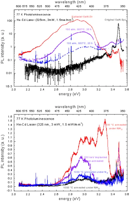
3.1. High Pressure Annealed Samples
The PL spectra of the samples varied widely as a function of the annealing conditions. Three unannealed samples were also measured to enhance the comparison. The highest PL efficiency (Figure 1) obtained in Zn-implanted GaN was achieved for material annealed for 20 hours under 190 atm. of N2 at 950 °C. Broad (FWHM ~ 75 nm) donor to Zn acceptor PL centered near 435 nm dominates the spectrum, but an excitonic transition near the GaN bandedge is also evident. The peak intensity was slightly more than an order of magnitude weaker than the epitaxially doped GaN:Zn control sample which was grown with a Zn concentration and distribution roughly comparable to the
implanted samples. The PL efficiency of the best RTA GaN:Zn annealed under flowing N2[14] was several times less than that of the sample annealed at 190 atm, 950 °C for 20 h, when taking the epitaxial sample as a common
reference. High pressure annealing at 900 °C resulted in a decade reduction of the PL efficiency compared to the 950 °C sample, while blistering was apparent on samples annealed at 1000 °C and high pressure. Due to our limited access to the high pressure annealing setup, we have made no effort to determine the effect of varied annealing times and pressure, although either might further improve the optical quality of Zn-implanted GaN.
3.2. Atmospheric Pressure Annealed Samples
All of the samples annealed in the atmospheric pressure MOCVD exhibited lower efficiency (i.e. <2 orders of magnitude below the epitaxial GaN:Zn standard) Zn PL (Figure 2). Only the sample annealed at 1100 °C under NH3 had improved PL compared to an unannealed Zn-implanted sample. No further improvement was realized in the NH 3 annealed samples when they were further annealed at 700 °C under N2 in an effort to remove any lingering H passivation. Comparing the 1100 °C/NH3 and unannealed samples, it is interesting to note that shorter wavelength transitions appear after the annealing. We have no explanation for this behavior at present.
Samples annealed at 1000 °C had inferior optical properties compared to the un-annealed Zn-implanted sample. The sample annealed at 1000 °C under N2 showed slightly more PL than that annealed under NH3, but we place this difference within the experimental error. Annealing under N2 at 1100 °C was not performed, since prior experience
[14] indicates that the sample blisters under these conditions.
4. High Resolution X-ray Diffractometry Data
4.1. X-Ray Rocking Curves
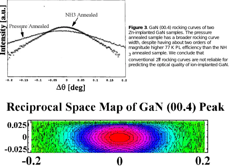
Standard HRXRD in the 2θ mode is very sensitive to implant damage. However, the fact that there are two GaN polytypes promotes stacking faults and twinning defects which also affect the peak widths. The Zn-implanted GaN samples studied here showed only minor sample to sample variation when measured using ω-2θ scans. Furthermore what small variation was observed, did not correlate with the optical measurements.
For example, Figure 3 compares two Zn-implanted GaN samples annealed under various conditions. The rocking curve width of the pressure annealed sample, the same which produced the highest PL efficiency, is actually
broader than that of an NH3 annealed sample whose PL is roughly 2 orders of magnitude less efficient. We conclude that were not able to reliably detect implant damage annealing without taking additional complicated steps such as taking into account the influence of twins and stacking faults.
4.2. Reciprocal Space Mapping
A promising technique for the study of orientational and twinning effects in heteroepitaxial structures is reciprocal space mapping (RSM). RSM is realized by adding a Ge crystal (the analyzer) between the sample and the detector to select the diffracted beam over a small angular range. Reciprocal space maps are useful for studying less perfect structures because they enable a separation of the effects of the lattice strain variations, curvature, and lattice orientations on the reciprocal space Bragg peak broadening.
To study the crystallographic orientation of a heteroepitaxial thin GaN film RSM by a four circle diffractometer was applied. Figure 4 shows the data of the GaN (00.4) peak from the high pressure annealed (190 atm, 950 °C) GaN:Zn sample which produced the best PL efficiency to date among our Zn-implanted GaN sample set.
The ∆ω axis in figure 4 of the map results from scanning the reciprocal space (00.4) point in the direction
perpendicular to the sample surface, while the ∆2θ axis corresponds to the direction parallel to the surface. The GaN peak broadening along the ∆2θ direction indicates lower coherence, probably caused by some defects and twinning effects. A detailed description is given in Appendix A of [15]. Figure 4 shows clearly that the FWHM depends strongly on the direction of the scan in the reciprocal space.
It is therefore important to describe clearly how rocking curves are measured. To our knowledge no commercial software package is able to calculate rocking curves in the wurzite structure. Therefore we can use rocking curve measurements only as a relative measurement to study changes in the strain as a function of dose, annealing temperature, and time. To obtain a complete picture, we should therefore try to correlate the triple axis scans to the PL measurements.
5. Discussion
The improved results obtained by annealing under nitrogen overpressure compared to atmospheric pressure support our earlier conclusion [14] that the optical activation of Zn impurities in GaN by thermal annealing is limited by N loss from the GaN crystal, and that a trade-off exists between the ability to anneal out implantation damage and activate dopants while maintaining stoichiometry. This is supported by our observation of the highest PL
efficiencies in samples annealed under either RTA or high pressure. This conclusion is also intuitive.
In the case of RTA, dopant activation and defect annealing take place on successively shorter time scales than N loss. This makes this technique useful for the electrical activation of Mg, Si or Ca dopants in GaN [7][8], and
moderately successful in the optical activation of GaN:Zn [14], as well as a standard technique in GaAs and InP-based device processing. While a high percentage of implanted dopants can be electrically activated by RTA of GaN [7], our previous GaN:Zn data [14] indicate that significant disturbance of the implanted region of the crystal remains after the RTA procedure. This will result in lower mobility material and reduced transistor performance.
The previous work of Pankove [5] on the optical activation of ion-implanted Zn acceptors was accomplished using atmospheric NH3 annealing. Similar experiments at the time using N2 gas yielded inferior material, whereas NH3 annealed samples had comparable PL to the epitaxial material of that time [16]. There exists no published quantitative measurements on these samples, nor does there exist a common reference sample with which to compare our data to Pankove’s. Nevertheless, our data indicate that NH3 offers little improvement towards the optical activation of implanted impurities, even when post-annealed in N2 to remove H.
The high pressure data described above are reasonably consistent with the pressure-temperature phase diagram of GaN measured by Karpinski et al. [17] who observed that the 190 atm. equilibrium line between GaN and Ga + N2 lies at roughly 1100 °C. It is probable that sufficient N was lost from the GaN crystal at 1000 °C to blister the SiNx cap layer, since damaged material (such as our implanted samples) is known to decompose at lower temperatures than higher quality samples [18]. If this is true, then the optical quality of the 950 °C annealed sample is limited by either N loss or insufficient defect annealing at this temperature. Regardless, it is probable that further improvement could
g p g , p p
be realized by annealing implanted GaN at higher pressure and temperature. In fact, ultrahigh pressure annealing of ion implanted GaN could be a viable solution to the ion-implantation problem in GaN, provided that structural
improvement can be realized at temperatures below those at which the implanted impurities begin to diffuse.
6. Conclusion
Our data indicate that N loss from GaN is the major obstacle to realizing ion-implanted GaN of high optical quality. Material of the highest optical quality in our laboratory to date was obtained by annealing at 950 °C and 190 atm. N2 overpressure, although it exhibited roughly an order of magnitude lower 77 K PL efficiency than comparable doped epitaxial GaN:Zn. GaN:Zn annealed for an hour under NH3 at atmospheric pressure showed slight improvement in both its optical and structural qualities compared to un-annealed implanted GaN:Zn and material annealed under N2 at atmospheric pressure, but all GaN:Zn annealed at atmospheric pressure had lower optical efficiency than pressure annealed samples. It would be very interesting to observe the optical quality of this material when annealed at yet higher pressure and temperature, such as the conditions used for bulk GaN crystal growth.
Acknowledgments
We gratefully acknowledge the contributions of P. W. Epperlein, A. Rockett and R. F. Broom to earlier stages of this study. We also thank P. Baumgartner for performing the Zn ion-implantation.
References
[1] S. Strite, H. Morkoç, J. Vac. Sci. Technol. B 10, 1237-1266 (1992).
[2] V. A. Dmitriev, Ya. V. Morozenko, I. V. Popov, A. V. Suvorov, A. L. Syrkin, V. E. Chelnokov, Sov. Tech. Phys. Lett. 12, 221 (1986).
[3] S. Strite, Monolithic Array of LEDs for the Generation of Light at Multiple Wavelengths and its use for Multicolor Display Applications, World Intellectual Property Organization Patent Number 11498 (1996) .
[4] J. I. Pankove, J. A. Hutchby, J. Appl. Phys. 47, 5387 (1976).
[5] J. I. Pankove, J. A. Hutchby, Appl. Phys. Lett. 24, 281 (1974).
[6] R. D. Metcalfe, D. Wickenden, W. C. Clark, J.Lumin. 16, 405 (1978).
[7] S. J. Pearton, C. B. Vartuli , J. C. Zolper , C. Yuan, R. A. Stall , Appl. Phys. Lett. 67, 1435-1437 (1995).
[8] J. W. Lee, S. J. Pearton , J. C. Zolper , R. A. Stall , Appl. Phys. Lett. 68, 2102-2104 (1996).
[9] R. G. Wilson , S. J. Pearton, C. R. Abernathy , J. M. Zavada , Appl. Phys. Lett. 66, 2238-2240 (1995).
[10] J. C. Zolper, M. Hagerott-Crawford, S. J. Pearton, C. R. Abernathy, C. B. Vartuli, C. Yuan, R. A. Stall, J. Electron. Mater. 25, 839-844 (1996).
[11] R. G. Wilson, C. B. Vartuli, C. R. Abernathy, S. J. Pearton, J. M. Zavada, Sol. St. Electr. 38, 1329-1333 (1995).
[12] S. C. Binari, H. B. Dietrich, G. Kelner, L. B. Rowland, K. Doverspike , D. K. Wickenden , J. Appl. Phys. 78, 3008-3011 (1995).
[13] J. C. Zolper , R. G. Wilson , S. J. Pearton , R. A. Stall , Appl. Phys. Lett. 68, 1945-1947 (1996).
[14] S. Strite, P. W. Epperlein, A. Dommann, A. Rockett, R. F. Broom, Mater. Res. Soc. Symp. Proc. 395, 795-800 (1996).
[15]N. Herres, F. Fuch, J. Schmitz, K. M. Pavlov, J. Wagner, J. D. Ralston, P. Koidl, C. Gadaleta, G. Scamarcio, "Effect of interfacial bonding on the structural and vibrational properties of InAs/GaSb superlattices," Phys. Rev. B
g p p p , y 53 (1996) 15688-15705
[16]J. I. Pankove, private communication
[17] J. Karpinski, J. Jun, S. Porowski, J. Cryst. Growth 66, 1 (1984).
[18]I. Grzegory, private communication
Figure 1. PL data taken at 77 K on GaN samples having reasonable optical quality. The epitaxial GaN:Zn intensity has been multiplied by a factor of 2.5 in this figure to offset a 40% lower PL excitation energy density. The PL spectrum of the original GaN/sapphire epitaxial material is plotted, although its emission is at the bandedge, and cannot be directly compared to the blue emission intensities exhibited by the Zn-doped GaN.
Figure 2. PL data taken at 77 K on GaN samples having lower optical quality than Figure 1. Only the sample annealed at 1100 °C under NH3 had improved PL efficiency compared to an un-annealed Zn-implanted control sample.
Figure 3. GaN (00.4) rocking curves of two Zn-implanted GaN samples. The pressure annealed sample has a broader rocking curve width, despite having about two orders of magnitude higher 77 K PL efficiency than the NH 3 annealed sample. We conclude that
conventional 2θ rocking curves are not reliable for predicting the optical quality of ion-implanted GaN.
Figure 4. Reciprocal space map of a GaN (00.4) peak from the high pressure annealed Zn-implanted GaN sample. The scan is plotted as logarithmic isointensity lines around the reciprocal lattice point. The x-axis represents ∆ω and
the y-axis is ∆2θ. © 1997 The Materials Research Society