HAL Id: hal-01307100
https://hal.sorbonne-universite.fr/hal-01307100
Submitted on 26 Apr 2016
HAL is a multi-disciplinary open access
archive for the deposit and dissemination of
sci-entific research documents, whether they are
pub-lished or not. The documents may come from
teaching and research institutions in France or
abroad, or from public or private research centers.
L’archive ouverte pluridisciplinaire HAL, est
destinée au dépôt et à la diffusion de documents
scientifiques de niveau recherche, publiés ou non,
émanant des établissements d’enseignement et de
recherche français ou étrangers, des laboratoires
publics ou privés.
Distributed under a Creative Commons Attribution| 4.0 International License
Multicharacterization approach for studying
InAl(Ga)N/Al(Ga)N/GaN heterostructures for high
electron mobility transistors
G Naresh-Kumar, A Vilalta-Clemente, S Pandey, D Skuridina, H
Behmenburg, P Gamarra, G Patriarche, I Vickridge, M. -A. Diforte-Poisson,
P Vogt, et al.
To cite this version:
G Naresh-Kumar, A Vilalta-Clemente, S Pandey, D Skuridina, H Behmenburg, et al..
Multichar-acterization approach for studying InAl(Ga)N/Al(Ga)N/GaN heterostructures for high electron
mo-bility transistors. AIP Advances, American Institute of Physics- AIP Publishing LLC, 2014, 4 (12),
pp.127101. �10.1063/1.4903227�. �hal-01307100�
for high electron mobility transistors
G. Naresh-Kumar, A. Vilalta-Clemente, S. Pandey, D. Skuridina, H. Behmenburg, P. Gamarra, G. Patriarche, I. Vickridge, M. A. di Forte-Poisson, P. Vogt, M. Kneissl, M. Morales, P. Ruterana, A. Cavallini, D. Cavalcoli, C. Giesen, M. Heuken, and C. Trager-Cowan
Citation: AIP Advances 4, 127101 (2014); doi: 10.1063/1.4903227
View online: http://dx.doi.org/10.1063/1.4903227
View Table of Contents: http://scitation.aip.org/content/aip/journal/adva/4/12?ver=pdfcov Published by the AIP Publishing
Articles you may be interested in
Thermal stability and in situ SiN passivation of InAlN/GaN high electron mobility heterostructures Appl. Phys. Lett. 105, 112101 (2014); 10.1063/1.4895807
Ultrathin InAlN/GaN heterostructures on sapphire for high on/off current ratio high electron mobility transistors J. Appl. Phys. 113, 214503 (2013); 10.1063/1.4808260
AlGaN/GaN two-dimensional-electron gas heterostructures on 200 mm diameter Si(111) Appl. Phys. Lett. 101, 082110 (2012); 10.1063/1.4746751
Electrical properties of InAlN/GaN high electron mobility transistor with Al 2 O 3 , ZrO 2 , and GdScO 3 gate dielectrics
J. Vac. Sci. Technol. B 29, 01A808 (2011); 10.1116/1.3521506
Compositional variation of nearly lattice-matched InAlGaN alloys for high electron mobility transistors Appl. Phys. Lett. 96, 252108 (2010); 10.1063/1.3456561
AIP ADVANCES 4, 127101 (2014)
Multicharacterization approach for studying
InAl(Ga)N/Al(Ga)N/GaN heterostructures for high
electron mobility transistors
G. Naresh-Kumar,1,aA. Vilalta-Clemente,2S. Pandey,3D. Skuridina,4
H. Behmenburg,5P. Gamarra,6G. Patriarche,7I. Vickridge,8
M. A. di Forte-Poisson,6P. Vogt,4M. Kneissl,4M. Morales,2P. Ruterana,2
A. Cavallini,3D. Cavalcoli,3C. Giesen,5M. Heuken,5and C. Trager-Cowan1
1Dept of Physics, SUPA, University of Strathclyde, Glasgow G4 0NG, UK 2CIMAP UMR 6252 CNRS-ENSICAEN-CEA-UCBN 14050 Caen Cedex, France 3Dipartimento di Fisica Astronomia, Università di Bologna, 40127 Bologna, Italy 4Institute of Solid State Physics, Technical University Berlin, 10623 Berlin, Germany 5AIXTRON SE, Kaiserstr. 98, 52134 Herzogenrath, Germany
6Thales Research and Technology, III-V Lab, 91460 Marcoussis, France 7LPN, Route de Nozay, 91460 Marcoussis, France
8Institut des NanoSciences, Université Pierre et Marie Curie, 75015 Paris, France
(Received 21 August 2014; accepted 19 November 2014; published online 1 December 2014)
We report on our multi–pronged approach to understand the structural and electri-cal properties of an InAl(Ga)N(33nm barrier)/Al(Ga)N(1nm interlayer)/GaN(3µm)/ AlN(100nm)/Al2O3high electron mobility transistor (HEMT) heterostructure grown
by metal organic vapor phase epitaxy (MOVPE). In particular we reveal and discuss the role of unintentional Ga incorporation in the barrier and also in the inter-layer. The observation of unintentional Ga incorporation by using energy dispersive X–ray spectroscopy analysis in a scanning transmission electron microscope is sup-ported with results obtained for samples with a range of AlN interlayer thicknesses grown under both the showerhead as well as the horizontal type MOVPE reactors. Poisson–Schrödinger simulations show that for high Ga incorporation in the Al(Ga)N interlayer, an additional triangular well with very small depth may be exhibited in parallel to the main 2–DEG channel. The presence of this additional channel may cause parasitic conduction and severe issues in device characteristics and processing. Producing a HEMT structure with InAlGaN as the barrier and AlGaN as the inter-layer with appropriate alloy composition may be a possible route to optimization, as it might be difficult to avoid Ga incorporation while continuously depositing the layers using the MOVPE growth method. Our present work shows the necessity of a multicharacterization approach to correlate structural and electrical properties to understand device structures and their performance. C 2014 Author(s). All article
content, except where otherwise noted, is licensed under a Creative Commons Attri-bution 3.0 Unported License.[http://dx.doi.org/10.1063/1.4903227]
I. INTRODUCTION
InAlN possesses the widest bandgap range in the nitride system and is thus an ideal material for applications in light emitting diodes, laser diodes and solar cells operating from the ultra vio-let to the near infrared.1,2In addition to this, the InAlN in In
xAl1−xN/GaN heterostructures can be
either under tensile or compressive strain depending on the In composition; this cannot be imple-mented in AlxGa1−xN/GaN heterostructures.1,3 The possibility of polarization matching with GaN
makes InAlN more attractive for high frequency transistor applications4and InAlN can also be lattice
aE mail:[email protected]
matched with GaN when the In composition is ≈ 18% which makes it a strong candidate for high elec-tron mobility transistors (HEMTs).5Unlike InGaN/GaN and AlGaN/GaN structures, the production of high quality InAlN/GaN HEMTs presents many growth challenges. In the nitride ternary alloys the optimum growth temperatures of the end compounds are quite different, especially using metal organic vapor phase epitaxy (MOVPE), i.e. AlN (> 1200◦C), GaN (≈ 1000◦C), and InN (< 550◦).
This is also the case for their covalent bond lengths;6therefore, the growth conditions need to be very well controlled indeed, such phenomena as the predicted miscibility gap in these alloys7may lead to phase separation,8,9ordering,10–12composition fluctuations13,14and even growth disruption.15Poor growth conditions can give rise to layers containing high densities of crystallographic defects16–19and even cracks.20Recently unintentional Ga incorporation in the InAlN layers has been reported which adds to the list of growth challenges for InAlN thin films.21–24There are two possible explanations given for the unintentional Ga incorporation in the InAlN layers. It can be either due to diffusion of Ga from the GaN buffer layers22or due to residual Ga in the growth chamber.23,24The latter seems to be more plausible from the recent work of Smith et al24and the possibility of Ga incorporation in the HEMT structures was also reported by Leach et al in 2010.25
Unintentional incorporation of Ga in the InAlN based HEMTs can be detrimental to the con-trol of the alloy composition and the optimization of growth conditions and it therefore becomes difficult to characterize these structures and understand their physical properties. Thus in order to understand the real properties of the unintentional Ga incorporated structures and samples with varying alloy composition; it becomes necessary to use a multitude of characterization techniques. On the optimistic side, the presence of Ga in the barrier (top epilayer) can be an advantage. As an alternative to InAlN or AlGaN as a barrier, quaternary InAlGaN layers have advantages to offer such as independently tailoring the band gap and lattice constant. By using InAlGaN, one can overcome the high strain state observed in the AlGaN barrier and alloy disordering/scattering issues in InAlN barriers. HEMTs with mobility greater than 1700 cm2V−1s−1and 2–DEG density of
1.8 × 1013cm−2have been reported for InAlGaN barriers.26
In this present work, we report on Ga incorporation both in the barrier (InAlN) as well in the interlayer (AlN) with a range of thicknesses, for samples grown in both the horizontal as well as close coupled shower head MOVPE reactors. Possible routes to minimize unintentional Ga incorpo-ration and the role of unintentional Ga incorpoincorpo-ration on the HEMT properties are also discussed.
II. EXPERIMENTAL
All the HEMT structures described in this work were grown by MOVPE. Two sets of sam-ples (A and B) were grown using an Aixtron 3 × 2 inch close coupled showerhead reactor while samples (C and D) were grown using an Aixtron 200 RF horizontal reactor. Figure 1 shows the schematic of the HEMT structures. Please note for the sake of clarity most of our discussion will focus on sample–A. We will discuss this sample’s structural, compositional and electrical prop-erties. Samples (B–D) were used to demonstrate the unintentional Ga incorporation both in the barrier and in the interlayer for the two different reactor designs. Samples A and B were grown on a 2–inch c–plane sapphire substrate using the standard precursors of trimethylgallium (TMGa), trimethylindium (TMIn) and ammonia (NH3) with H2as the carrier gas. For sample–A, the growth
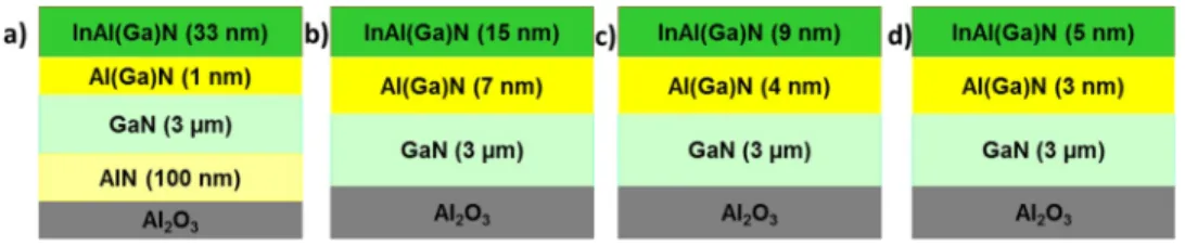
FIG. 1. Schematic of the HEMT structures, (a) sample–A and (b) sample–B were grown in the close coupled shower head reactor, (c) Sample–C and (d) sample–D were grown in the horizontal reactor.
127101-3 Naresh-Kumar et al. AIP Advances 4, 127101 (2014)
was initiated by depositing an AlN nucleation layer with a thickness of 6 nm deposited at 780◦C,
followed by 94 nm of AlN and 3 µm of GaN, these buffer layers, were grown at 1250◦C and 1070◦C
respectively. Sample–B was grown under the same conditions as sample–A, but without the AlN buffer layer. The growth surface temperature was monitored by an in situ reflectivity measurement tool from LayTec instruments, which simultaneously measures the reflectivity at different wave-lengths (276 nm to 775 nm). A thin AlN layer (interlayer of 1 nm for sample–A and 7 nm for sample–B) followed by an InAlN layer (barrier of 33 nm for sample–A and 15 nm for sample–B) were grown at 790◦C. Please note that both the barrier and the interlayer were grown at the same
temperature. The reactor pressure was maintained at 70 mbar with a V–III ratio of 5000. Samples–C and D were grown on a 2–inch c–plane sapphire substrate using TMGa, TMIn and NH3as
precur-sors with both H2and N2as the carrier gases. These samples do not have an AlN nucleation layer
as in sample–A; however there is similar GaN buffer layer of 3 µm grown at 1150◦C. The AlN
interlayer (4 nm for sample–C and 3 nm for sample–D) were grown at 1200◦C with a reactor
pressure of 50 mbar with H2as a carrier gas followed by the deposition of an InAlN barrier (9 nm
for sample–C and 5 nm for sample–D) grown at 865◦C with N2as the carrier gas with a reactor
pressure of 70 mbar. The V–III ratio was kept at 2200. The target composition of the barrier layers was In0.18Al0.82N, i.e., the composition which provides a lattice match to GaN.
Structural characterization of sample–A was performed using various microscopy techniques. A Digital Instruments Nanoscope III atomic force microscope (AFM), operating under tapping mode using a Si cantilever, was used to image the topography and also to determine the surface roughness. An FEI–Sirion–200 field–emission gun scanning electron microscope (SEM) operating under secondary electron (SE) imaging mode was used to image surface morphology and electron channelling contrast imaging (ECCI) performed in the forescatter geometry was used to image grain boundaries and structural defects. Both SE and ECC images were acquired with an elec-tron beam spot of ≈ 4 nm, a beam current of ≈ 2.5 nA, beam divergence of ≈ 4 mrad and an acceleration voltage of 30 keV. Transmission electron microscopy was used for detailed analysis of layer thicknesses, threading dislocations (TDs) types, and other structural defects.27,28A JEOL 2010 transmission electron microscope (TEM) operated at 200 keV was used to carry out plan view as well as cross section analyses. An aberration corrected JEOL 2200 scanning transmission electron microscope (STEM) operated at 200 kV with a probe current of 150 pA and a probe size of 0.12 nm at the full width at half maximum (FWHM) was used for high angle annular dark field (HAADF) imaging at the sub nanometer scale for determining the structure and composition of the interface between the barrier, interlayer and the GaN buffer layer. The convergence half-angle of the electron probe was 30 mrad and the detection inner and outer half-angles for the HAADF-STEM images were 100 and 170 mrad, respectively. The plan view and cross section samples for TEM and STEM–HAADF were prepared by tripod polishing down to around 10 µm, with electron trans-parency achieved using a Gatan ion polishing system. Ar+beam milling was performed with the sample tilted ≈ 4◦at 5 keV. During the ion milling process, the sample holder was always kept at
-150 C in order to minimize the ion beam damage and a final step of milling was carried out at 0.7 keV to remove the amorphous layers.
The alloy composition for sample–A was estimated from high resolution X–ray diffraction (HRXRD), Rutherford backscattering spectrometry in the channelling geometry (RBS/C) and X–ray photoelectron spectroscopy (XPS) measurements. Energy dispersive X–ray analysis (EDX) in the STEM provided compositional information on nanoscale. Quantitative measurements of the composition were obtained with EDX from the intensity ratio of the K line of Al (1.486 keV), the K line of Ga (9.770 keV) and L line of In (3.290 keV). The K line of elementary N (0.392 keV) was also taken into account. Each EDX spectrum was acquired for 60 seconds using JEOL 2300D detectors. The k–factors used by the computer software were calibrated using reference samples of AlN and AlGaN/GaN epitaxially grown on a Si substrate. The composition of the (Al,Ga)N alloys used for the calibration was precisely determined by XRD. The k–factors used for In was cali-brated using InP, In0.48Al0.52As and In0.53Ga0.47As ternary alloys. All the calibration samples were
prepared in a Focused Ion Beam SEM (section thicknesses were estimated to be between 60 and 80 nm). HRXRD measurements were performed using an X’Pert MRD triple axis diffractometer equipped with a four-bounce (220)–Ge monochromator and operating at the Cu Kα1wavelength of
1.54056 Å. RBS/C was performed using a 1.6 MeV4He+beam with a nominal incidence and a
scat-tering angle of 165◦and the random RBS spectrum was fitted using the SIMNRA software.29XPS was performed under ultra–high vacuum (UHV) conditions using a PHOIBOS100 energy analyzer and monochromated Al Kα(hv= 1486.9 eV) radiation as an X–ray source with an instrumental
resolution set to be ≈ 400 meV.
Electrical characterization for sample–A was performed to investigate the 2–DEG related prop-erties. Room–temperature (R–T) Hall measurements were performed in the Van der Pauw geometry and capacitance–voltage (C–V) measurements at R–T were performed using Ti/Al/Ni/Au based ohmic contacts (dots of 0.6 mm diameter) and Ni/Au Schottky diode contacts (dots of 1 mm diameter) at an operating frequency of 1 KHz.
III. RESULTS AND DISCUSSION
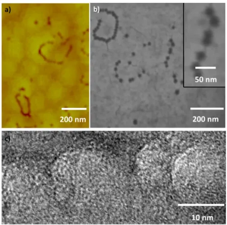
Figure2shows plan view AFM, SEM and TEM images of the V–pits/defects. The AFM image in Fig.2(a)shows a smooth surface morphology with rounded hillock features,30typical for InAlN thin films grown by MOVPE.1The root–mean–square (rms) roughness for a 5µm × 5µm area was estimated to be 0.8 nm (image not shown here). The total V–defect density estimated from AFM, SEM and plan view TEM images are 1.1±0.2×109 cm−2, 2.4±1×109 cm−2and 4.5±2×109cm−2
respectively. The difference in the V–defect density is probably due to the different length scales used in the three different techniques, images with an area of 1 µm2(for AFM) 8.5 µm2(for SEM)
and 0.1 µm2(for TEM) were used to estimate the V–defect density. Care has to be taken in
esti-mating the V–defect density as different techniques at dissimilar length scales with different scan areas can provide varying results. In the present case the results obtained were of the same of order
FIG. 2. (a) AFM, (b) plan view SE and (c) plan view TEM images of sample-A showing individual and clustering of V–defects.
127101-5 Naresh-Kumar et al. AIP Advances 4, 127101 (2014)
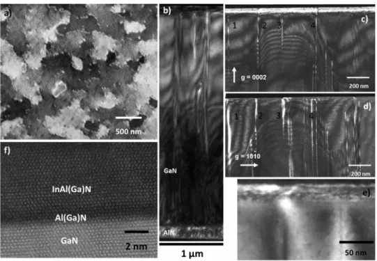
FIG. 3. (a) Electron channelling contrast image showing V–defects decorating the grain boundaries (b) 2–beam dark field image (0002 reflection) revealing the AlN and GaN buffer layer (c) 0002 reflection (d) 10-10 reflection showing TDs propagating to the surface and connected to V–defects (e) high magnification image showing V-defect connected to a TD and a TD which is not connected to a V-defect (f) High–angle annular dark field image revealing a smooth interface between the AlN and GaN as well as the InAl(Ga)N layer.
of magnitude in spite of the areas sampled varying by two orders of magnitude. More information on using different imaging techniques for the determination of TD densities can be found from the work of Khoury et al.31 In order to gain further insight on the structural properties, ECCI was performed. More information on the ECCI technique can be found elsewhere.32–35Figure3(a) shows an electron channelling contrast image revealing low angle tilt or rotation boundaries with V–defects decorating the boundaries and also inside the grains. Dislocations may be located on a grain boundary and the presence of V–defects on the grain boundaries indicates that they could be related to the TDs. The total defect density estimated from ECC images with a scan area of 17 µm2
was 5±1 × 109cm−2.
Cross section TEM was performed to estimate layer thickness and identify dislocation types. Fig.3(b)shows a two beam dark field image taken with (0002) reflections where a large number of TDs can be seen in the AlN and GaN buffer layers. It can be seen clearly that there are more TDs in the AlN buffer when compared to GaN and thus the inclusion of AlN buffer helps in reducing the TD density. TDs propagating to the surface, which are connected to V–defects, were imaged using (0002) and (10-10) reflections respectively as shown in Fig.3(c) and3(d). A high magnification image revealing a TD connected to a V–defect is shown in Fig.3(e). Many areas of the sample were analyzed by cross–section TEM and it was found that there are ≈ 50% pure edge dislocations and ≈ 50% mixed dislocations, no pure screw dislocations were observed in the analyzed areas. High magnification HAADF images were recorded to reveal the crystalline quality of the layers at the atomic scale, the structure of the interfaces and to determine the AlN interlayer thickness. This is clearly shown in Fig.3(f)which exhibits a smooth interface between the Al(Ga)N and GaN as well as the InAl(Ga)N. These images also reveal some variation in the intensity for different alloys which qualitatively implies that the composition may not be uniform from one column to the next. In order to estimate a realistic alloy distribution, detailed compositional analysis was carried out by several techniques.
Figure4shows the (000l) HRXRD θ–2θ scan for all the expected peaks of InAl(Ga)N, GaN, AlN and Al2O3. From the HRXRD, the c–plane lattice constant was found to be 0.507 nm and by
FIG. 4. HRXRD θ-2θ diagram of InAl(Ga)N/Al(Ga)N/GaN/AlN on Al2O3substrate.
using the corrected Vegard’s law,36 the In content was estimated to be 13.25 %. With knowledge of the c–plane lattice parameter and the strain state of the layer, one can accurately estimate the alloy composition for a ternary (e.g. InAlN). However, HRXRD cannot accurately estimate the compositions of quaternaries (e.g. InAlGaN) as the fitting will allow a range of compositions for fully strained layers; hence alternative techniques such as RBS become necessary. RBS allows the determination of the composition profile of thin films with a depth resolution of a few nanometers and additional structural information can be provided when combined with the ion channelling phenomena. Ion channelling takes place when the beam is aligned with a major symmetry direc-tion of the crystal producing an intense reducdirec-tion of the backscattering signal. The ratio between aligned and random yield is called the minimum yield (χmin) and can be used as an indicator of the
crystalline quality.37Figure5illustrates RBS/C random (line), the corresponding fit (triangles), and
127101-7 Naresh-Kumar et al. AIP Advances 4, 127101 (2014) <0001> aligned spectra (circles). The In signal is in the 1360-1400 keV energy range in the RBS spectrum whereas the Al signal is at 855-890 keV and the Ga signal at 1270 keV. The In signal is completely separated from the GaN substrate signal in the spectrum, which gives an accurate measurement of the In concentration. The In content in the barrier was estimated to be 12% and no phase separation was evident from RBS measurements. Moreover, in agreement with the TEM observations where no misfit dislocations could be observed, it is clear that these InAl(Ga)N layers have grown coherently on the Al(Ga)N/GaN structures. The inset in Fig.5magnifies the spectrum for the energy region between 1320 keV to 1420 keV which corresponds to the backscattered signal from In atoms with a χminvalue of 7%. There is a small change in the slope at around 1250 keV
which is due to the presence of Ga in the InAlN layer. From RBS/C it is clearly evident that the barrier has Ga incorporation and the Ga composition was estimated to be ≈ 32%, the Al composi-tion was estimated to be ≈ 56 %. RBS has an elemental depth resolucomposi-tion of 5nm – 50 nm with an uncertainty in the range of 1 – 5% for compositional analysis.
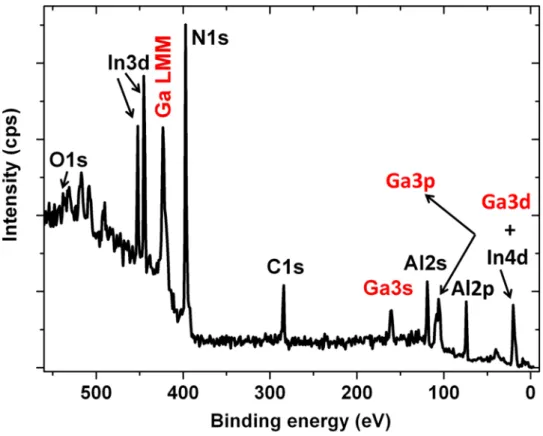
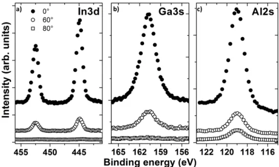
In order to confirm the presence of Ga, XPS measurements were performed. The sampling depth can be changed according to the angle between the sample surface and the photoelectron emission, i.e., the take–off angle. Quantitative analysis of the elemental composition was based on the determination of the peak area with corresponding sensitivity factors. Despite the high annealing temperature (650◦C), significant carbon contamination remained on the sample surface as is shown in the spectrum in Fig.6. The core–level peaks corresponding to electronic states of the elements in the barrier layer are shown clearly in Fig. 6. Besides the Al, In, and N atoms contributing to the layer and surface contaminants (carbon and oxygen), the spectrum contains a single Ga Auger (160.8 eV) and a core–level photoelectron peak (423.2 eV), confirming Ga incorporation in the bar-rier layer. In order to determine the amount of Ga within the barbar-rier, surface sensitive measurements were performed at take–off angles of 60◦and 80◦. Angle–resolved high resolution spectra of the In
3d, Ga 3s and Al 2s core–level peaks are shown in Fig.7. At 80◦the Al component dominates the
FIG. 6. XPS spectrum from the barrier layer of sample–A after annealing at 650◦C under UHV conditions. The core-level
FIG. 7. The XPS core-level spectra from sample-A a) In 3d, b) Ga 3s, c) Al 2s recorded at take-off angles of 0◦
, 60◦and 80◦respectively after annealing at 650◦C.
spectra and there is not much contribution from the Ga or In signal. The quantitative calculations re-vealed a Al0.68In0.07Ga0.25N elemental composition for measurements at 0◦, indicating a Ga
contri-bution of 25% compared to 7% of In. High surface sensitive measurements performed at 60◦and
80◦exhibited alloy compositions of Al
0.70In0.06Ga0.25N and Al0.93In0.01Ga0.06N, respectively. Thus,
gallium incorporation of ≈ 25% within the barrier seems reasonable apart from the very surface region, where the surface is Al–terminated. Please note that although XPS is a quantitative tech-nique, producing accurate atomic concentrations from the XPS spectra is not straightforward. The intensities measured using XPS from similar samples are repeatable to good precision, but the technique has an accuracy of 10% for performing routine atomic concentrations. From RBS and XPS measurements, the presence of Ga in the barrier is thus irrefutable; it then becomes obvious to question if there is also unintentional Ga in the interlayer. To investigate this, high resolution EDX measurements were performed.
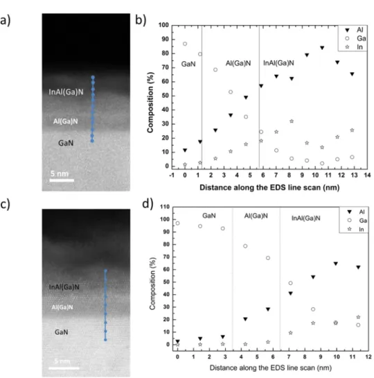
The alloy composition as a function of sample depth (along the growth direction) was measured with EDX in a STEM. Figure8(a)shows a STEM–HAADF micrograph where a three layer struc-ture is clearly observed, the bright contrast layer corresponding to GaN, the faintly dark strip of ≈ 1 nm at the interface corresponding to AlN and the uniform lighter contrast layer towards the sur-face corresponding to the 33 nm of InAl(Ga)N. The composition of the three layers was analyzed along the growth direction by performing an EDX line scan. The blue line scan in Fig.8(a)shows the probe position during the EDX acquisition, where twelve points were analyzed across the three layers and the corresponding composition is shown in Fig.8(b). The first point corresponds to the GaN buffer layer which shows the highest Ga content and the second point corresponds to the ≈1 nm, AlN interlayer which also shows a Ga composition of 84% and a Al composition of 36% which strongly indicates that the interlayer is Ga rich Al(Ga)N. The composition starts to decrease as the line scan moves towards the barrier and thereafter does not change appreciably. We have also mapped the Ga composition along the barrier layer (parallel to the growth direction, 10 nm from the interface) which exhibits a reasonably high Ga content of ≈ 45%. There is a slight fluctuation of In composi-tion between 8% to 13% along the growth direccomposi-tion in the barrier layer. The Indium content for this structure (sample–A) determined by HRXRD and RBS was estimated to be 13.25% and 12% respec-tively. From the STEM–EDX analysis we deduce that there is ≈ 11% of InN in the barrier. In order to check the reliability of our measurements of Ga incorporation in the AlN interlayer, STEM–EDX was performed on sample–B with a 7 nm AlN interlayer, this is shown in Fig.8(c)and8(d). The HAADF–STEM image of sample–B shows four different regions with different grey scale for layers
127101-9 Naresh-Kumar et al. AIP Advances 4, 127101 (2014)
FIG. 8. (a) Cross section HAADF-STEM image, the dotted line shows the position of the EDX line scan across the InAl(Ga)N/Al(Ga)N/GaN heterostructure, (b) the corresponding EDX profiles showing the Al, Ga and In composition as a function of position, (c) HAADF-STEM image of the thicker interlayer sample, the dotted line shows the position of the EDX line scan from the substrate to the surface and (d) the corresponding EDX profiles showing Al, Ga and In composition as a function of position.
with different compositions as shown in Fig.8(c). For the interlayer, two distinct layers of AlN are observed in this sample, the reason for the presence of the two layers is not clear. However, the line scan across the growth direction clearly shows the presence of Ga in the interlayer (points 3 to 6). The first two points correspond to the GaN buffer layer and the Ga content starts to decrease from 72% to 48% as the line scan proceeds across the 7 nm interlayer. On the other hand, the Al content starts to increase from 28% to 52% implying the varying of both the Ga and Al composition. Thus from our detailed analysis it becomes clear that there is Ga incorporation even in the interlayer in addition to the barrier. Inside the barrier layer for sample–B, the Al content decreases and at the same time the Ga content increases and both show a composition of 50%. Please note for sample–A, the Ga composition estimated by EDX is higher (≈ 45 %) when compared to RBS (≈ 32 %), this can be explained due to the fact that RBS gives information on a larger area whereas EDX is probing on the atomic scale. In addition there are local composition fluctuations of ≈ 10 % depending on the probed area. The accuracy of the EDX analysis is estimated to be about 1% (except for nitrogen, where the precision is ± 2%).38
Following the observation of unintentional Ga incorporation in the barrier as well as in the interlayer for samples grown using the close coupled shower head MOVPE reactor, we also per-formed measurements to see if there are any unintentional Ga incorporation for samples grown using a horizontal MOVPE reactor. Fig.9 shows the HAADF–EDX results for samples C and D.
FIG. 9. Sample grown in a horizontal MOVPE reactor (a) and (c) Cross section HAADF images, the lines indicate the position of the EDX line scans across the heterostructures and (b) and (d) the corresponding Al, Ga and In composition as a function of position.
The line scan along the growth direction reveals the presence of Ga both in the interlayer as well as in the barrier. For sample–C in the interlayer, the Ga composition decreases from ≈ 80% at the GaN interface to ≈ 20% at the top of the interlayer and for sample–D in the interlayer, the Ga composition decreases from ≈ 80% at the GaN interface to ≈ 50% at the top of the interlayer. In the barrier layers we observe a decreasing trend of Ga incorporation along the growth direction and at 5 nm from the interface, the detected highest Ga content was less than 3% for sample–C (see Fig.
9(b)), and 10% for sample–D (see Fig.9(d)).
Hiroki et al proposed a possible explanation for unintentional Ga incorporation in the barrier.21 According to them, the metallic Ga which can remain on the flow distributor in the reactor may give rise to a chemical reaction between the TMIn which is provided for the InAlN growth. Similar explanations were given by Choi et al39and Kim et al23where they explain the origin of uninten-tional Ga is believed to be from the surrounding surfaces in the growth chamber and from the wafer susceptor. An imperfect source–gas switching sequence can also cause contamination in the layers but for the layers investigated in the present work, we may rule out this possibility. In our case at the end of the GaN growth the TMGa was switched off and the temperature and NH3flow were then
ramped to reach the AlN growth conditions and growth recommenced using the TMAl and NH3
precursors. The growth of the AlN takes about 2 minutes and at the end of the growth, the TMIn flow was switched on and the temperature decreased to the InAlN growth conditions. In our process, the TMGa is switched off for 6 minutes before beginning the growth of InAlN. Thus we believe all
127101-11 Naresh-Kumar et al. AIP Advances 4, 127101 (2014)
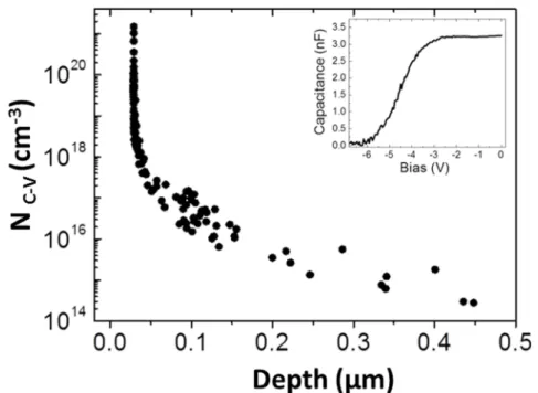
FIG. 10. Apparent free carrier concentration against depth showing the sharp increase related to presence of the 2-DEG at the InAl(Ga)N/Al(Ga)GaN interface. The C-V profile acquired at 1 KHz against reverse bias is also shown in the inset, this evidences the depletion of the 2-DEG.
the TMGa is evacuated from the growth chamber before the growth of InAlN. To the best of our knowledge there are no reports on the Ga incorporation in the interlayer and all the published work on Ga incorporation is on samples grown under closed coupled shower head reactors. In our case, we have Ga incorporation in samples grown using both types of reactors. Interrupting the growth and cleaning the reactor prior to growing the interlayer and barrier may be a route to reduce the unintentional Ga incorporation as described by Hiroki et al;21however this may not be practicable. Future work is necessary to understand the role of reactor designs to reduce/eliminate unintentional Ga incorporation.
To investigate the role of Ga incorporation in the barrier and in the interlayer on the HEMTs characteristics, we carried out electrical measurements for sample–A. The 2–DEG density value was found to be ≈ 3.02 x 1013cm−2and the R–T Hall mobility is ≈ 980 cm2/V-s and sheet resistance is ≈ 210 Ohm/sq. Our structure shows reasonably good values related to 2–DEG properties with high density and low sheet resistance which is an indication of a good heterointerface.
The apparent free carrier concentration profile and C–V plot measured at R–T are shown in Fig.10and in the inset of Fig.10respectively. The carrier concentration depth profile was calcu-lated using the procedure proposed in ref.40. The depth profile evidences the maximum value of the free carriers at the Al(Ga)N/GaN interface, hence indicating the presence of the 2–DEG at the interface. The background carrier concentration related to the GaN layer was also estimated to be of the order of 1016cm−3. It should be noted that the precision of the extracted carrier depth profile could suffer with some error due to the increasing Debye length (λD) with decreasing electron
density towards the GaN layer.41The 2–DEG density value estimated from the C–V plot was found to be ≈ 3.2 x 1013cm−2by using the method described in ref.42. The obtained values were in good agreement with Hall measurements and are similar to earlier reported results on InAlN/AlN/GaN based structures.43
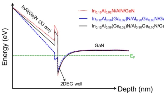
In order to understand the impact of the presence of unintentional Ga in the barrier and in the interlayer on the band structure, we have simulated the band diagrams for three structures with and without Ga in the barrier and interlayer by using nextnano simulation software.44Fig.11shows the schematic representation of the simulated band structure for the ideal case of the lattice matched In0.18Al0.82N/AlN/GaN structure,4for sample–A with high Ga in barrier and interlayer (80%) and
FIG. 11. Schematic representation of the simulated band diagrams for InAl(Ga)N/Al(Ga)N/GaN heterostructures for a structure without Ga diffusion (round dotted line), structures with high/low Ga diffusion in barrier and interlayer (solid line and square dotted line).
finally a structure with low Ga (≈10%) in the interlayer with a quarternary barrier similar to that measured for sample–A, i.e., (In ≈ 12 %, Al ≈ 56 % and Ga ≈ 32 %). We have observed the expected 2–DEG triangular well formation at AlN/GaN interface for all structures but surprisingly the presence of another well was also observed in parallel to 2–DEG well for the structure (sample–A) with high Ga (80%) in interlayer. The existence of a narrow and a weak parallel well for the structure with a high Ga (80%) containing interlayer may be due to a very small band offset between barrier layer and interlayer which bends the conduction band below the Fermi level at InAl(Ga)N/Al(Ga)N interface. The presence of this unexpected well might influence the 2–DEG concentration and mobility values. However for sample–A, we have still achieved a good value for the 2–DEG density and mobility at 300 K, which may be due to the fact this 2ndwell is relatively much weaker than the main 2DEG well and its screening effect might not significantly influence 2–DEG properties. A similar observation with two–channel conduction in InAlN/AlN/GaN structures due to the presence of an unexpected thin parasitic GaN layer has also been reported in the literature.25The presence of unintentional Ga could influence the 2–DEG electronic properties of the HEMT structures and also can create some issues on fabricating and operating HEMT devices with good device characteristics.
IV. CONCLUSIONS
From our experimental results acquired by using various characterization techniques we have verified the presence of unintentional Ga in the barrier as well as in the interlayer for samples grown using both closed coupled and horizontal MOVPE reactors. In spite of sample–A having a defect density in the order of 109cm−2and high Ga incorporation in the interlayer, the mobility
and 2–DEG density are comparable to good quality samples. We surmise that this reasonably high mobility is due to the smooth interfaces between the Al(Ga)N/GaN and InAl(Ga)N as revealed by STEM. The existence of a narrow, weak well parallel to the main 2–DEG well for the structure with high (80%) Ga content in the interlayer (sample–A) was observed in the 1–D Poisson–Schrödinger simulations. No such additional 2–DEG well was observed for structure with 10% of Ga in the interlayer. The existence of unintentional Ga in the HEMT structures does not appreciably affect the 2–DEG properties; however it could be a problem during device processing. Stopping the growth and cleaning the MOVPE reactors prior to growing the interlayer and barrier may help in reducing the unintentional Ga incorporation, but may not be a practical feasible solution. On the other hand producing a HEMT structure with InAlGaN as a barrier and the AlGaN as an interlayer with
127101-13 Naresh-Kumar et al. AIP Advances 4, 127101 (2014)
appropriate alloy composition may be a possible route to optimization as it might be difficult to avoid Ga incorporation while continuously depositing the layers using the MOVPE growth method. The present work shows the importance of using a multicharacterization approach to have a better understanding of materials properties, especially for samples with varying alloy composition and complex physical properties.
ACKNOWLEDGMENTS
This work was supported by the EU project no. PITN–GA–2008–213238 (RAINBOW) and the EPSRC project EP/J015792/1. Naresh-Kumar would like to thank Prof. Peter Parbrook from the University College Cork, Ireland for his valuable discussions.
1R Butte et al.,J. Phys. D: Appl. Phys.40, 6328 (2007).
2A. Castiglia, E. Feltin, G. Cosendey, A. Altoukhov, J.-F. Carlin, R. Bute, and N. Grandjean,Appl. Phys. Lett.94, 193506
(2009).
3J. Kuzmik,Semicond. Sci. Technol.17, 540 (2002).
4S. Choi, H. J. Kim, Z. Lochner, Y. Zhang, Y. C. Lee, S. C. Shen, J. H. Ryou, and R. D. Dupuis,Appl. Phys. Lett.96, 243506
(2010).
5M. Gonschorek, J.-F. Carlin, E. Feltin, M. A. Py, and Grandjean,Appl. Phys. Lett.89, 062106 (2006). 6Z. Dridi, B. Bouhafs, and P. Ruterana,Semicond. Sci. and Technol.18, 850 (2003).
7B. P. Burton, A. van de Walle, and U. Kattner,J. Appl. Phys.100, 113528 (2006).
8M. D. McCluskey, L. T. Romano, B. S. Krusor, D. P. Bour, and N. M. Johnson,Appl. Phys. Lett.72, 1730 (1998). 9A. Redondo-Cubero, K. Lorenz, R. Gago, N. Franco, M-A di Forte Poisson, E. Alves, and E. Munoz,J. Phys. D: Appl.
Phys.43, 055406 (2010).
10P. Ruterana, G. Nouet, W. Van der Stricht, I. Moerman, and L. Considine,Appl. Phys. Lett.72, 1742 (1998). 11D. Korakakis, K. F. Ludwig, Jr., and T. D. Moustakas,Appl. Phys. Lett.71, 72 (1997).
12P. Ruterana, G. de Saint Jores, S. Laugt, and F. Omnes,Appl. Phys. Lett.78, 344 (2001).
13Z. Gacevic, S. Fernandez-Garrido, J. M. Rebled, S. Estrade, F. Peiro, and E. Calleja,Appl. Phys. Lett.99, 031103 (2011). 14P. Ruterana, S. Kret, A. Vivet, G. Maciejewski, and P. Dluzewski,J. Appl. Phys.91, 8979 (2002).
15G. Perillat-Merceroz, G. Cosendey, J. F. Carlin, R. Butte, and N. Grandjean,J. Appl. Phys.113, 063506 (2013). 16V. Potin, P. Vermaut, P. Ruterana, and G. Nouet,J. Electronic Materials27, 266 (1998).
17P. Vermaut, G. Nouet, and P. Ruterana,Appl. Phys. Lett.74, 694 (1999). 18V. Potin, G. Nouet, and P. Ruterana,Appl. Phys. Lett.74, 947 (1999).
19Q. Y. Wei, T. Li, Y. Huang, J. Y. Huang, Z. T. Chen, T. Egawa, and F. A. Ponce,Appl. Phys. lett100, 092101 (2012). 20A. Minj, D. Cavalcoli, and A. Cavallini,J. Phys.: Conf. Ser.326, 012011 (2011).
21M. Hiroki et al.,J. Cryst. Growth382, 36 (2013). 22J. J. Zhu et al.,J. Cryst. Growth348, 25 (2012). 23J. Kim et al.,J. Cryst. Growth388, 143 (2014). 24M. D. Smith et al.,J. Mater. Chem. C2, 5787 (2014). 25J. H. Leach et al.,J. Appl. Phys.107, 083706 (2010). 26N. Ketteniss et al.,Semicond. Sci. Technol.25, 075013 (2010).
27P. Vermaut, P. Ruterana, G. Nouet, and H. Morkoç, Inst. Phys. Conf. Ser. 146, 289 (1995). 28P. Ruterana and G. Nouet,Phys. Stat. Sol. B227, 177 (2001).
29M. Mayer,AIP Conf. Proc.474, 541 (1999).
30A. Vilalta-Clemente et al.,Phys Status Solidi A207, 1105 (2010). 31M. Khoury et al.,Semicond. Sci. Technol.28, 035006 (2013).
32D. C. Joy, D. E. Newbury, and D. L. Davidson,J. Appl. Phys.53, 81 (1982). 33C. Trager-Cowan et al.,Phy. Rev. B75, 085301 (2007).
34G. Naresh-Kumar et al.,Phys. Stat. Sol. A209, 424 (2012). 35G. Naresh- Kumar et al.,Phys. Rev. Lett.108, 135503 (2012).
36K. Lorenz, N. Franco, E. Alves, I. M. Watson, R. W. Martin, and K. P. O’Donnell,Phys. Rev. Lett.97, 085501 (2006). 37A. Redondo-Cubero et al.,J. Phys. D: Appl. Phys.43, 055406 (2010).
38K. Pantzas et al.,Nanotechnology23, 455707 (2012). 39S. Choi et al.,J. Cryst. Growth388, 137 (2014).
40O. Ambacher, J. Smart, J. R. Shealy, N. G. Weimann, K. Chu, M. Murphy, W. J. Schaff, L. F. Eastman, R. Dimitrov,
L. Wittmer, M. Stutzmann, W. Rieger, and J. Hilsenbeck,J. of Appl. Phys.85, 3222 (1999).
41D. K. Schroder, Semiconductor material and device characterization, 3rd. ed. (IEEE Press, Wiley, 2006). 42S. Pandey, B. Fraboni, D. Cavalcoli, A. Cavallini, T. Brazzini, and F. Calle,Appl. Phys. Lett.100, 152116 (2012). 43M. Gonschorek, J. F. Carlin, E. Feltin, M. A. Py, N. Grandjean, V. Darakchieva, B. Monemar, M. Lorenz, and G. Ramm,
J. Appl. Phys.103, 093714 (2008).