HAL Id: hal-01444949
https://hal.archives-ouvertes.fr/hal-01444949
Submitted on 24 Jan 2017HAL is a multi-disciplinary open access archive for the deposit and dissemination of sci-entific research documents, whether they are pub-lished or not. The documents may come from teaching and research institutions in France or abroad, or from public or private research centers.
L’archive ouverte pluridisciplinaire HAL, est destinée au dépôt et à la diffusion de documents scientifiques de niveau recherche, publiés ou non, émanant des établissements d’enseignement et de recherche français ou étrangers, des laboratoires publics ou privés.
Optimizing magneto-optical effects in the ferromagnetic
semiconductor GaMnAs
Hassen Riahi, L. Thevenard, Mhamed Maaref, Bruno Gallas, Aristide
Lemaître, Catherine Gourdon
To cite this version:
Hassen Riahi, L. Thevenard, Mhamed Maaref, Bruno Gallas, Aristide Lemaître, et al.. Optimizing magneto-optical effects in the ferromagnetic semiconductor GaMnAs. Journal of Magnetism and Magnetic Materials, Elsevier, 2015, 395, pp.340 - 344. �10.1016/j.jmmm.2015.07.090�. �hal-01444949�
1
Optimizing magneto-optical effects in the ferromagnetic
semiconductor GaMnAs
H.Riahi a*, L. Thevenardb,c, M. A. Maaref a, B. Gallasb,c, A. Lemaîtred,C. Gourdonb,c
a Laboratoire Matériaux Molécules et Applications, IPEST, Université de Carthage, La Marsa, Tunisie
b CNRS, UMR7588, Institut des Nanosciences de Paris, 4 place Jussieu, 75005 Paris, France
cSorbonne Universités, UPMC Université Paris 06, UMR7588, 4 place Jussieu, 75005 Paris, France.
d Laboratoire de Photonique et de Nanostructures – CNRS, Route de Nozay, 91460 Marcoussis, France.
e-mail: [email protected] Keywords : magnetic semiconductors, magneto-optical Kerr effect
Abstract:
A trilayer of the ferromagnetic semiconductor GaMnAs, a SiO2 buffer layer and a
piezoelectric ZnO layer, is investigated in view of its use in device implementation to study surface acoustic wave-assisted magnetization switching. The magneto-optical properties: Kerr rotation and ellipticity and magnetic contrast in Kerr microscopy images are investigated as a function of temperature. While the ZnO layer prevents any good quality imaging of magnetic domains, we show that with the SiO2 layer only the
polar Kerr rotation and the magnetic contrast are increased by a factor of 2. This result is in good quantitative agreement with calculations using an optical interference model and could be further improved. The detrimental effects of the dielectric layers capping on the Curie temperature and coercive field of the GaMnAs layer can be kept to a reasonable level.
1. Introduction :
The ferromagnetic semi-conductor (Ga,Mn)As has received considerable attention in the recent years, as a promising material for future semiconductor spintronic devices [1,2]. It has become a test-bed material for magnetization manipulation by static strain [3,4], electric field [5], light pulses, [6, 7, 8, 9], acoustic (strain) pulses [10, 11], and very recently by surface acoustic waves (SAW) [12,13]. This has been made possible thanks to the large sensitivity of the magnetic anisotropy to strain [14, 15]. Strain waves like SAWs have been identified as a powerful tool for magnetization switching in magneto-strictive materials [16, 17, 18]. In GaMnAs, it was recently demonstrated that magnetization precession can be resonantly driven by a SAW when both the magnon and phonon frequencies match [13], which is the first necessary step towards precessional switching
[12]. The most direct evidence for magnetization switching can be obtained from
magneto-optical imaging using Kerr microscopy (KM) based on the rotation of the linear polarization of light upon reflection on a magnetized sample [19, 20]. However, the Kerr
2
rotation angle is usually no more than a fraction of degree in GaMnAs [21]. Therefore, differential imaging and an exposure time of the order of 1 s have to be used [22]. It is well known that this rotation angle and thus the magnetic contrast can be enhanced by using multiple reflections in an additional anti-reflecting dielectric layer deposited onto the surface of metallic magnetic samples [19, 23, 24, 25]. However, this has not yet been evidenced with magnetic semiconductors in which the typical penetration depth of light can be of several hundreds of nm. Dielectric layers are also needed for SAW generation and detection. Since GaMnAs is weakly piezoelectric, interdigitated metallic transducers combs for SAW generation and detection need to be patterned onto a piezoelectric ZnO layer evaporated at high temperature (150-250°C) on GaMnAs with a Si02 buffer layer.
However, this process might be detrimental since the magnetic properties of the GaMnAs layer highly depend on strain and heat treatment [22].
The point is then to take advantage of these dielectric layers to optimize the magnetic contrast while keeping the detrimental effect of this capping as low as possible.
In this paper, we investigate the wavelength and temperature dependence of the magneto-optical properties of a GaMnAs layer with and without capping by dielectric layers using polar magneto-optical Kerr effect (PMOKE).
2 - Sample and experimental setup
The sample is a 50 nm thick Ga1-xMnxAs (x= 0.07) layer grown on a (Ga,In)As relaxed
buffer layer deposited on a semi-insulating (001) GaAs substrate in order to achieve perpendicular magnetic easy axis [22,26]. The (Ga,Mn)As layer was deposited at 250 ° C. After the growth, the sample was thermally annealed at 250°C for 1 hour in order to improve its magnetic properties.
From SQUID magnetometry the Curie temperature was found to be 116 K and the active Mn concentration was about 3.3 %. One sample was kept as a reference (GaMnAs-ref). On one part of the second sample (named GaMnAs/SiO2/ZnO) a SiO2(80 nm)/ZnO (250nm)
bilayer was grown by radio-frequency sputtering. The rest of the sample was masked during the growth of the dielectric layers. Care was taken to keep the sample holder at relatively low temperature (150°C) in order not to further anneal the GaMnAs layer. The masked GaMnAs part (GaMnAs-h) is nevertheless checked. After optical investigation, the ZnO layer was removed with HCl leaving a GaMnAs/SiO2 part. Eventually, SiO2 was
further removed by hydrofluoric acid.
MOKE measurements were performed in the polar geometry with the light beam at quasi-normal incidence on the sample surface. Monochromated light from a 150 W Xe lamp was polarized with a Glan-Thompson polarizer, chopped at f0=250 Hz by a mechanical chopper
and phase-modulated at f=50 kHz by a photo-elastic modulator (PEM). The beam reflected off the sample passed through an analyzer, and was detected by a Si photodiode whose signal was fed into lock-in amplifiers. The signal at f0 provided a measurement of the
average light intensity at each wavelength. The Kerr rotation angle θK and the ellipticity ηK
were obtained from the signals at 2f and f, respectively, following the procedure described in Ref. [27]. The sample was kept in a helium-flow cryostat, allowing the temperature T to be varied from 10 to 300 K. An external magnetic field was applied perpendicular to the sample surface and could be swept between −20 mT and +20 mT. The KM images were obtained using a polarizing microscope in reflection geometry. The sample was illuminated at = 670 nm, close to the maximum of the Kerr rotation angle. Hysteresis cycle can be obtained by averaging the signal over each image while scanning the magnetic field. Details can be found elsewhere [22].
3
3- Results and discussion
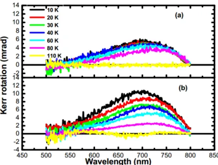
Fig.1. Kerr rotation spectra at different temperatures for GaMnAs (a) and GaMnAs/SiO2
(b) layers.
First, samples GaMnAs-ref, GaMnAs-h, and GaMnAs/SiO2/ZnO were studied. Hysteresis
cycles were obtained from KM images at T=30 K. The first two samples show very similar hysteresis cycles. The coercive field was the same (2.5 mT) however the saturation field was larger for GaMnAs-h indicating that the heating process has created defects acting as domain-wall pinning centers. The coercive field was slightly larger for GaMnAs/SiO2/ZnO
(3.3 mT instead of 2.5 mT), so was the saturation field. In this sample, the magnetic contrast between the up and down magnetized states is similar to GaMnAs-h however the details of the magnetic domains pattern could hardly be distinguished. These results mean that in future SAW devices, the ZnO layer will have to be removed between the generating and detecting interdigitated combs in order to allow magneto-optical imaging of domains in the GaMnAs layer. We will therefore now concentrate on the magneto-optical properties of the different zones of the sample after ZnO removal, namely GaMnAs/SiO2 and
GaMnAs-h, hereafter simply called GaMnAs.
PMOKE spectra are shown in Fig. 1 for GaMnAs/SiO2 and GaMnAs. For both zones, the
spectral dependence of the Kerr rotation K is similar with a maximum around 704 nm. It is
clear that the Kerr rotation is enhanced by a factor 2 at T=10 K for GaMnAs/SiO2 with
respect to GaMnAs. Such an effect, which will be discussed in more details in the next section, was already observed for other ferromagnetic materials (TbFe and GdTbFeCo with a-Si:0 [23], NiFe with ZnS [24]). MgO and SiNx capping layers on CoFe have also been
investigated [25].
The amplitude of θK decreases with temperature. This point will addressed more
quantitatively below.
Figure 2 shows the ellipticity ηK versus wavelength for both samples at T=10 K. Both
4
the θK peak. The ellipticity (in absolute value) is larger than the Kerr rotation (about 20
mrad at the dip position) however the enhancement with the SiO2 layer is not as high as for
the Kerr rotation (21 mrad instead of 18 mrad at the dip position) in agreement with calculations (see below).
In order to assess the usefulness of the SiO2 capping layer in the operating conditions for
SAW devices we take Kerr images of the magnetic domains at different temperatures from
T=30 K to T=90 K for GaMnAs/SiO2 and GaMnAs layers (Fig.3).
In each image of Fig. 3, the GaMnAs and GaMnAs/SiO2 zones are on the left and right
parts of the image, respectively, as delimited by the dashed line. The sample edge is shown by the full line. These images are differential images. The reference is taken with the magnetization fully saturated in one direction. Therefore, the reversed domains appear on a uniform background. As typically observed for GaMnAs grown on a GaInAs pseudo-substrate [22], magnetization reversal proceeds with the nucleation and growth of dendritic like domains branching along the [110] and [-110] crystallographic directions. The contrast between the up and down states of magnetization is defined as
C=2(I+-I-)/(I++I-) where I+ and I- are the intensities of up and down magnetized domains,
respectively. At T=31 K domains appear as much brighter for GaMnAs/SiO2. The
magnetic contrast is enhanced from 5.6 % to 11.3 %, i.e. by a factor of 2, with the SiO2
capping layer on GaMnAs. However, the nucleation of domains and their expansion is more difficult, in agreement with the slightly larger coercive field and higher field needed to reach saturation. At higher temperature, domain nucleation occurs at the sample edge and propagation is not impeded.
Fig.2. Ellipticity as a function of wavelength at T= 10 K for GaMnAs (black empty
5
Fig.3.Snapshots of the magnetic domain structure observed by KM in a temperature range 30 K - 90 K, on the GaMnAs layer with and without SiO2 capping layer (right and left side
of the dashed line, respectively). The sample edge is shown by a full line. Here, the magnetic contrast has been digitally enhanced with respect to the original images for the sake of clarity
6
Fig.4. Dependence of the Kerr rotation peak amplitude (open circles) and the magnetic contrast of Kerr images (solid squares) on the temperature for GaMnAs (a) and GaMnAs/SiO2 (b) layers.
Figure 4 shows the magnetic contrast of Kerr images together with the peak of the Kerr rotation angle obtained from PMOKE as a function of temperature for GaMnAs (Fig. 4 (a)) and GaMnAs/Si02 (Fig. 4 (b)). The magnetic contrast follows the same temperature
dependence as the Kerr rotation. The proportionality factors between the contrast and the Kerr angle are not exactly identical for GaMnAs and GaMnAs/SiO2 but close (1.2 and 1.5,
respectively), although they should theoretically be equal in our experimental conditions. For GaMnAs/SiO2, the contrast drops to zero at T=90 K, indicating a reduction of the
Curie temperature from 116 K to 90 K. A similar drop of TC has also been found from
electrical measurements of the SAW attenuation and velocity change in a SAW-driven ferromagnetic resonance experiment in GaMnAsP [13]. After full removal of the SiO2
layer, TC remains at 93 K indicating that irreversible damages were produced as could also
be found from X-rays measurements on a similar sample [13].
4- Model
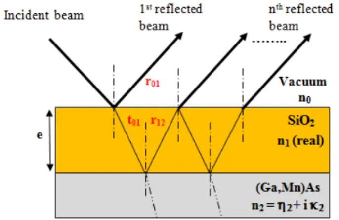
Fig.5.Schematic illustration of a model based on optical interferences in (Ga,Mn)As/SiO2
structure. For the sake of clarity, the experimentally near-normal incidence light beam is shown here with a large incidence angle.
The experimental results will be discussed in the framework of an optical interference model as schematically depicted in Fig. 5. We assume that the GaMnAs layer has an infinite thickness, i.e. we do not take into account reflection at the substrate interface, which is weak owing to a very small difference of refractive indices [11]. The refractive index n1 (real) of the silica layer is taken from [28]. The wavelength dependence of the real
and imaginary parts of the GaMnAs refractive index n2=2+i2 are obtained from
ellipsometry measurements on a similar sample at room temperature. The amplitude reflection coefficient at normal incidence is written as:
7
where r01=(1-n1)/(1+n1) and r12=(n1-n2)/(n1-n2) are the amplitude reflection coefficients at
the vacuum/SiO2 interface and at the SiO2/GaMnAs interface respectively. e is the SiO2
thickness and t is equal to 4n1/ with the wavelength. It is expected that in the
condition of anti-reflection, i.e. for a silica thickness close to a quarter of the wavelength in this material /(4n1), multiple reflections at the silica/GaMnAs interface will enhance the
Kerr rotation while decreasing the intensity of reflected light.
By minimizing the reflectance R=rr*, one deduces the expression of the optimal thickness of the SiO2 layer:
2 1 2 1 2 2 1 12 12 12 1 Im( ) 2 ) Re( 2n
n
ArcTan n r r r ArcTan n eopt (2)where Re (Im) denotes the real (imaginary) part, respectively, and the approximate expression assumes a weak absorption in GaMnAs (2 <<(2,n1)). The optimal thickness
shown in the inset of Fig. 6, is found to be within a few percent (4.5 % to 1.8 %) of the quarter wavelength /(4n1) in the spectral range =500 nm to 800 nm.
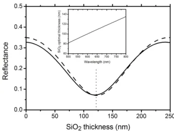
Fig. 6. Reflectance as a function of SiO2 thickness at the peak of Kerr rotation (=704 nm),
for normal incidence (full line) and 20° incidence (dashed line). The dotted vertical line shows the value of the SiO2 thickness equal to a quarter wavelength in the SiO2 layer
e=/(4n1). The inset shows the SiO2 thickness for minimum reflectance as a function of the
8
Fig. 7. Kerr rotation angle (solid line) and ellipticity (dashed-dotted line) at 704 nm (peak of the Kerr rotation) and T=10 K as a function of the SiO2 thickness from Eq. 3. The
arrows show the change of Kerr rotation and ellipticity from no SiO2 layer to a 80 nm SiO2
layer.
The calculated reflectance is shown in Fig. 6 at =704 nm (the peak of Kerr rotation) as a function of the silica thickness. The reflectance minimum is broad. The choice of the SiO2
thickness is therefore not critical. The thickness for minimum reflectance is 119 nm. The reflectance has also been calculated for an angle of incidence of 20° (the maximum incidence angle with the microscope objective used for KM). It is shown by the dashed line in Fig. 6. There is minor change with respect to normal incidence; which means that optimization of the silica thickness can be done without taking into account the numerical aperture of the objective.
The Kerr rotation and ellipticity are calculated as Re(K) and Im(K), respectively, where
K reads:
Θ (3)
where Q=Qr+iQi is the complex Kerr coefficient proportional to the saturation magnetization M. It is related to the off-diagonal element xy of the dielectric permittivity
tensor by xy=-i2 Q mz, with mz the component of the unit magnetization vector along the
normal to the sample surface and 2=n22 [19].The transmission coefficient t21 is equal to 2n2/(n1+n2).
The Qr and Qi values are obtained from the experimental Kerr rotation and ellipticity at
T=10 K. The dependence of the Kerr rotation and ellipticity on the SiO2 thickness at the
peak of Kerr rotation =704 nm is calculated and shown in Fig. 7. The arrows show the change of Kerr rotation and ellipticity from zero to 80 nm of silica. They are in good agreement with experimental results. One finds a change of the Kerr rotation from 5.6 mrad to 14 mrad (10.5 mrad experimentally) and of the ellipticity from -6.4 mrad to -7.8 mrad (-11 mrad experimentally). In particular, the increase of the Kerr rotation is larger than the increase of Kerr ellipticity (in absolute value), as found experimentally. The precise knowledge of the GaMnAs refractive index at low temperature would certainly improve the agreement with experimental results. One can note that the peak of Kerr rotation is found for a silica thickness of 106 nm, slightly smaller than the thickness for minimum reflectance (119 nm).
5- Conclusion:
In view of using dielectric SiO2 and ZnO layers as buffer layer and piezoelectric
transducer, respectively, for surface acoustic wave generation and detection on a ferromagnetic semiconductor, we have grown a GaMnAs/SiO2/ZnO sandwich and studied
its magneto-optical properties. The aim was to assess the possible detrimental changes of the magnetic properties after the growth of overlayers on the GaMnAs ferromagnetic layer and to improve magneto-optical imaging for the study of SAW-assisted magnetization reversal. Although the magnetic properties of the tri-layer were not seriously altered, the ZnO layer did not allow good quality imaging of the magnetic domains. In future SAW devices, the ZnO layer will have to be removed in a window between the two sets of excitation and detection interdigitated combs. With a SiO2 layer of 80 nm, the magnetic
9
contrast could be multiplied by 2. An optimized thickness of 106 nm should further increase the contrast. The temperature behavior of the magnetic contrast and the Kerr rotation angle has shown that the Curie temperature decreased from 116 K to 90 K with the SiO2 capping layer. This remains a problem but not too serious for SAW device operation.
More generally this work can serve as a basis for optimization of magnetic contrast in magnetic semiconductors, not only for the investigation of SAW induced magnetization switching but also for the study of domain patterns and domain wall dynamics.
Acknowledgement
We are grateful to J. Y. Duquesne from Institut des Nanosciences de Paris for the growth of the dielectric layers on GaMnAs. This work has been supported by Region Ile-de-France (DIM Nano-K MURAS2012), by Agence Nationale de la Recherche (ANR 2010-BLANC-0424-02 and ANR13-JS04-0001-01), and by the French RENATECH network. One of us, H. R., acknowledges financial support from the Ministry of Higher Education and Scientific Research of Tunisia.
10
[1] P. Němec, V. Novák, N. Tesařová, E. Rozkotová, H. Reichlová, D. Butkovičová, F. Trojánek, K. Olejník, P. Malý, R. P. Campion, B. L. Gallagher, J. Sinova, and T. Jungwirth, Nature 4 ( 2013) 1422.
[2] T. Dietl, and H. Ohno, Review of Modern Physics 86 (2014) 187.
[3] A. W. Rushforth, E. De Ranieri, J. Zemen, J. Wunderlich, K. W. Edmonds, C. S. King, E. Ahmad, R. P. Campion, C. T. Foxon, B. L. Gallagher, K. Výborný, J.Kučera, and T. Jungwirth, Physical Review B 78 (2008) 085314.
[4] A. Lemaître, A. Miard, L. Travers, O. Mauguin, L. Largeau, C. Gourdon, V. Jeudy, M. Tran, and J.-M. George. Applied Physics Letters 93 (2008) 021123.
[5] K. Olejník, M. H. S. Owen, V. Novák, J. Mašek, A. C. Irvine, J. Wunderlich, and T. Jungwirth, Physical Review B 78 (2008) 054403.
[6] A. V. Kimel, G. V. Astakhov, G. M. Schott, A. Kirilyuk, D. R. Yakovlev, G. Karczewski, W. Ossau, G. Schmidt, L. W. Molenkamp, and T. Rasing, Physical Review Letters 92 (2004) 237203.
[7] G. V. Astakhov, A. V. Kimel, G. M. Schott, A. A. Tsvetkov, A. Kirilyuk, D. R. Yakovlev, G. Karczewski, W. Ossau, G. Schmidt, L. W. Molenkamp, and Th. Rasing, Applied Physical Letters 86 (2005) 152506.
[8] Y. Hashimoto and H. Munekata, Applied Physical Letters 93 (2008) 202506.
[9] P. Němec, E. Rozkotová, N. Tesařová, F. Trojánek, E. De Ranieri, K. Olejník, J. Zemen, V. Novák, M. Cukr, P. Malý, and T. Jungwirth, Nature Physics8 (2012) 411- 415. [10] M.Bombeck, A. S. Salasyuk, B. A. Glavin, A. V. Scherbakov, C. Brüggemann, D. R. Yakovlev, V. F. Sapega, X. Liu, J. K. Furdyna, A. V. Akimov, and M. Bayer, Physical Review B 85 (2012) 195324.
[11] L. Thevenard, E. Peronne, C. Gourdon, C. Testelin, M. Cubukcu, E. Charron, S. Vincent, A. Lemaître, and B. Perrin, Physical Review B 82 (2010) 104422.
[12] L.Thevenard, J.-Y. Duquesne, E. Peronne, H. J. von Bardeleben, H. Jaffres, S. Ruttala, J-M. George, A. Lemaître, and C. Gourdon, Physical Review. B 87 (2013) 144402.
[13] L. Thevenard, C. Gourdon, J. Y. Prieur, H. J. von Bardeleben, S. Vincent, L. Becerra, L. Largeau, and J.-Y. Duquesne, Physical Review B 90 (2014) 094401.
[14] J. Zemen, J. Kucera, K. Olejník, and T. Jungwirth, Physical Review B 80 (2009) 155203.
[15] M. Glunk, J. Daeubler, L. Dreher,S. Schwaiger, W. Schoch, R. Sauer, W. Limmer, A. Brandlmaier, S. T. B. Goennenwein, C. Bihler and M. S. Brandt, Physical Review B 79(2009) 195206.
[16] W. Li, P. Dhagat, and A. Jander, IEEE Trans. Magn48 (2012) 4100.
[17] W. Li, B. Buford, A. Jander, and P. Dhagat, Journal of Applied Physics 115 (2014) 17E307.
[18] S. Davis, J. A. Borchers, B. B. Maranville, and S. Adenwalla, Journal of Applied Physics 117 (2015) 063904.
[19] A. Hubert and R.Schäfer, Magnetic domains, Springer, Berlin (2009).
[20] A.K Zvezdin and V.A Kotov, Modern magneto-optics and magneto-optical materials, Studies in Condensed Matter Physics, Taylor & Francis Group (New York), 1997.
[21] C. Sun, J. Kono, Y. -H. Cho, A. K. Wojcik, A. Belyanin, and H. Munekata, Physical Review B 83 (2011) 125206.
[22] A. Dourlat, V. Jeudy, C.Testelin, F. Bernardot, K. Khazen, C. Gourdon, L. Thevenard, L. Largeau, O. Mauguin, and A. Lemaître, Journal of Applied Physics102 (2007) 023913. [23] K. Nakamura, T. Asaka, S. Asari, Y. Ota, and A. Itoh, IEEE Transactions on Magnetics MAG-21 (1985) 1654.
11
[24] P. H. Lissberger, Journal of the Optical Society of America 51 (1961) 948, and references therein.
[25] K-M. Wu, J-F. Wang, K-C. Chen, J-C. Wu, and L. Horng. Journal of Magnetism and Magnetic Materials 310 (2007) e944–e946.
[26] L. Thevenard, L. Largeau, O. Mauguin, G. Patriarche, and A. Lemaître, Physical ReviewB 73 (2006) 195331.
[27] K. Sato, Japanese Journal of Applied Physics 20,(1981) 2403-2409.
12
Figure captions
Fig.2.Kerr rotation spectra at different temperatures for GaMnAs (a) and GaMnAs/SiO2 (b)
layers.
Fig.2. Ellipticity as a function of wavelength at T= 10 K for GaMnAs (black empty circles) and GaMnAs/SiO2 (red squares).
Fig.3. Snapshots of the magnetic domain structure observed by KM in a temperature range 30 K - 90 K, on the GaMnAs layer with and without SiO2 capping layer (right and left side of
the dashed line, respectively). The sample edge is shown by a full line. Here, the magnetic contrast has been digitally enhanced with respect to the original images for the sake of clarity.
Fig.4. Dependence of the Kerr rotation peak amplitude (open circles) and the magnetic contrast of Kerr images (solid squares) on the temperature for GaMnAs (a) and GaMnAs/SiO2 (b) layers.
Fig.5. Schematic illustration of a model based on optical interferences in (Ga,Mn)As/SiO2
structure. For the sake of clarity, the experimentally near-normal incidence light beam is shown here with a large incidence angle.
Fig. 6. Reflectance as a function of SiO2 thickness at the peak of Kerr rotation (=704 nm),
for normal incidence (full line) and 20° incidence (dashed line). The dotted vertical line shows the value of the SiO2 thickness equal to a quarter wavelength in the SiO2 layer
e=/(4n1). The inset shows the SiO2 thickness for minimum reflectance as a function of the
wavelength (Eq. 2).
Fig. 7. Kerr rotation angle (solid line) and ellipticity (dashed-dotted line) at 704 nm (peak of the Kerr rotation) and T=10K as a function of the SiO2 thickness from Eq. 3. The arrows