Development of Neural Probes Using Thermal
Drawing
by
Andres Canales
B.S. Chemistry, Universidad Nacional Aut6noma de M6xico (2011)
S.M, Massachusetts Institute of Technology (2013) SUBMITTED TO THE DEPATMENT OF
MATERIALS SCIENCE AND ENGINEERING
IN PARTIAL FULFILLMENT OF THE REQUIREMENTS
FOR THE DEGREE OF DOCTOR OF PHILOSOHPY
AT THE
MASSACHUSETTS INSTITUTE OF TECHNOLOGY
June, 2017
@2017 MASSACHUSETTS INSTITUTE OF TECHNOLOGY. ALL RIGHTS RESERVED
Signature of Author:_
Signature redacted
Department of Materials Science and Engineering May 11, 2017
Certified by:
Signature redacted
Polina Anikeeva Class of 1942 Associate Professor in Materials Science and Engineering Thesis Supervisor
______:Signature redacted
Accepted by:
MASSACHUSETS INSTUTE #I//onald R. Sadoway
Development of Neural Probes Using
Thermal Drawing
by
Andr6s Canales
Submitted to the Department of Materials Science and Engineering on May 11, 2017 in Partial Fulfillment of the Requirements for the Degree of
Doctor of Philosophy in Materials Science and Engineering
Abstract
The treatment of neurodegenerative and neurological conditions relies on better understanding the system that they afflict. However, the tools currently available to probe neural circuits are often limited to use in short-term studies primarily due to poor of biocompatibility. To address this challenge, flexible, minimally invasive neural probes were fabricated using a thermal drawing process, with polymers serv-ing as their main structural constituent. Through the use of different polymers, probes containing arrays of tin electrodes as small as 5 pm were fabricated, as were probes combining capabilities for electrical recording, optical stimulation, and drug delivery. A technique was developed to combine functionalities of these devices into a single probe to study the effect of optical stimulation with different waveforms on the brain activity. To break the longitudinal symmetry inherent to probes fabricated using the thermal drawing process, and to allow the incorporation of functionalities along the probe length, a method to combine thermal drawing with a method com-monly used to fabricate neural probes, photolithography, was developed, along with the selection of the polymer that would allow consecutive processing using these two techniques.
All of the fabricated probes were characterized and tested in vivo by
implanta-tion into mice and assessing their funcimplanta-tionality. High signal-to-noise ratio (13 6)
recordings were obtained using multielectrode arrays. Recordings of neural activ-ity during simultaneous optical stimulation and drug delivery were performed with multifunctional probes. Hybrid probes combining metal electrodes with a polymer waveguide were used to study the response of large groups of neurons to different forms of optical stimuli. Most importantly, the biocompatibility of these probes was assessed over a 3 month period and compared favorably to that of steel microwires of similar size.
Thesis Supervisor: Polina Anikeeva
Acknowledgements
There is nothing better for a man, than that he should eat and drink, and that he should make his soul enjoy good in his labour. This also I saw, that it was from the hand of God.
Ecclesiastes 2:24
The words quoted above have often been a source of inspiration during my time working in this thesis. Even in difficult times, they have helped me to keep a cheer-ful disposition. I'm also gratecheer-ful to all the people who have provided support during my time working on this thesis, and although a comprehensive list would be too long, there are some persons I would like to highlight.
First, I want to thank Prof. Polina Anikeeva for placing her trust in me to de-velop her vision of biocompatible neural probes into tangible devices. Her guidance throughout these years has helped me grow as a scientist and as a person. Further-more, she has shown concern for my well-being beyond what was expected, and for that I am forever grateful.
This work also benefited greatly from interactions with my colleagues working in the Bioelectronics group. In particular, I would like to thank those of you in my long list of coauthors for their invaluable contributions to the different projects on which we worked together: Dr. Ulrich Froriep, Dr. Ryan Koppes, Dr. Chi Lu, Dr. Xiaoting Jia, Christina Tringides, Jennifer Selvidge, Dr. Ritchie Chen, and Seongjun Park. I am grateful to my coauthors from other groups, both from MIT and outside, that played important roles in the realization of this work, including Dr. Chong Hou, Dr. Lei Wei, Dr. Yuanyuan Guo, and Dr. Benjamin Grena. Fi-nally, Antje Kilias, with whom I not only had the opportunity to coauthor a paper, but managed to have fun while doing the work.
Since the beginning of my thesis work, Prof. Yoel Fink has lent a great deal of support, not only by lending his equipment, which was essential for the project, but also through fruitful discussions in which he always provided honest feedback, which I deeply appreciate. I also thank people from the fibersamit group, both past and present, who have always been willing to help. The lessons on thermal drawing
provided by Dr. Alexander Stolyarov at the beginning proved to be vital for the rest of my work.
I also want to thank my collaborator Gregory Ellson, from Prof. Walter Voit's
group, for his help in finding an appropriate polymer that can be processed with both, thermal drawing and photolithography.
Throughout my time in the Bioelectronics group, I had the opportunity to work with and mentor several people. Each of those interactions taught me some lessons, and I benefited both academically and personally. Christina Tringides, Mina Hana, Jennifer Selvidge, Jeffrey Scully, and Matthew Forrester, I hope you benefited from our interactions as much as I did.
Although mentioned previously, I want to give special thanks to Dr. Ulrich Fror-iep for not only being a great collaborator and teaching me such a wide range of skills, but also for being a great friend. Thank you, and Gaby Froriep, for your support.
To my friends back home, it is always fun hanging out with you, and talking with you serves to remind me of the good times we've had together. Thank you, in particular to those of you who stayed in touch through all the time despite my occasional unresponsiveness.
Finally, I would like to thank my family, who have always provided me with vital support. In particular, I thank my parents, whose decision to get directly involved in my education since my early years by homeschooling me has led to the culmination of this work. Thank you for all your teachings, from which the academic ones are not the most important:
... whatever you do, do it all for the glory of God.
Contents
1 Introduction 10
1.1 The nervous system . . . 10
1.2 Development of neural engineering . . . 12
1.2.1 Bidirectional neural probes . . . 14
1.2.2 Failure modes of neural probes . . . 18
2 Fabrication Methods 23 2.1 Thermal drawing process . . . 23
2.2 Lithographic fabrication . . . 33
3 Design and fabrication of fiber-based probes 39 3.1 Multiwire arrays . . . 39
3.1.1 Thermal drawing process . . . 40
3.1.2 Minimizing the footprint . . . 42
3.1.3 Increasing the number of electrodes . . . 42
3.1.4 Connector . . . 45
3.2 Hybrid fiber probes for optogenetics and electrophysiology . . . 46
3.2.1 Thermal drawing process . . . 46
Contents
3.3 Multifunctional probes . . . 49
3.3.1 Thermal drawing process . . . 50
3.3.2 Connector . . . 52
3.4 Coupling thermal drawing with photolithography . . . 52
3.4.1 Material selection . . . 53
3.4.2 Polymer synthesis . . . 56
3.4.3 Film fabrication . . . 58
3.4.4 Polymer characterization . . . 59
3.4.5 Photolithographic patterning . . . 66
3.4.6 Thermal drawing process . . . 67
4 Characterization of neural probes 70 4.1 Mechanical . . . 70
4.2 Electrical . . . 71
4.3 Optical . . . 73
4.4 Microfluidic channel characterization . . . 77
5 Applications in neuroscience of fiber probes 78 5.1 Experimental setup . . . 78
5.1.1 Implantation of multiwire and multifunctional probes . . . 78
5.1.2 Data analysis . . . 80 5.2 Multiwire Arrays . . . 80 5.3 Analog optogenetics . . . 82 5.3.1 Experimental setup . . . 83 5.3.2 Results . . . 86 5.4 Trimodal function . . . .. . 93
5.5 Biocompatibility . . . 101
6 Discussion of key findings 108 6.1 Fiber-based fabrication of neural probes . . . 108
6.2 Multiwire arrays . . . 110
6.3 Hybrid probes . . . 112
6.4 Multifunctional probes . . . 115
6.5 Coupling TDP with photolithography . . . 117
6.6 Compatibility . . . 119
7 Conclusions and Outlook 121 7.1 Key lessons . . . 122
7.2 O utlook . . . 123
Bibliography 127
Abbreviations
mPFC: medial prefrontal cortex BADGE: Bisphenol A diglycidyl
ether
BBB: Blood brain barrier BIC: Bicuculline methiodide
CD68: Cluster of differentiation 68 CNQX:
6-cyano-7-nitroquinoxaline-2,3-dione
COC: Cyclic olefin copolymer CPE: carbon loaded polyethylene ChR2: Channelrhodopsin-2
DMA: Dynamical mechanical analysis DMPA:
2,2-Dimethoxy-2-phenylacetophenone DSC: Differential scanning
calorimetry
DV: Dorsoventral
GFAP: Glial fibrillary acidic protein HC: Hippocampus
Ibal: Ionized calcium-binding adaptor
molecule 1
IgG: Immunoglobulin G LFP: Local field potential
ML: Mediolateral
NMR: Nuclear magnetic resonance
PBS: Phosphate buffer solution PC: Polycarbonate
PCA: Principal component analysis PCB: Printed circuit board
PEI: Polyetherimide PPSU: Polyphenylsulfone RC: Rostrocaudal
SEM: Scanning electron microscope
SNR: Signal-to-noise ratio
TATATO:
1,3,5-triallyl-1,3,5-triazine-2,4,6(1H,3H,5H)-trione
TDP: Thermal drawing process TGA: Thermogravimetric analysis THF: Tetrahydrofuran TMICN: Tris[2-(3-mercaptopropionyloxy)ethyl] isocyanurate TPA: Tripropylamine WT: Wild type
1
Introduction
Understanding the mammalian nervous system is key to the development of treatments for neurological, neurodegenerative, psychiatric and neuromuscular con-ditions such as Parkinson's disease, Alzheimer's disease and multiple sclerosis. This, however, still remains a challenge since our ability to not only to record, but also to manipulate the nervous system remains limited. Significant effort has been made to produce neural activity recording devices with high precision and resolution over the past three decades. Despite important advances in the fabrication of the neural probes useful in short-term experiments [Bruno and Simons, 2002; Buzsiki et al.,
1992; Hafting et al., 2005; Hochberg et al., 20061, and the progress in fabrication
methods and materials, seamless integration of these devices into the surrounding tissues has not yet been achieved (Fig. 1.1).
1.1 The nervous system
The nervous system, consisting of the brain, the spinal cord and the periph-eral nerves, contains, billions of neurons communicating with each other through quadrillions of synapses [Kandel et al., 20001. Neurons make up ~ 50 % of the cells in the brain, the rest consisting of electrically inactive cells called glia [Azevedo et al.,
1.1 The nervous system
a Genetic
Fin ha2d.eins |Ch j2.ap
Green fluorescent protein IFluorescent ion indicators CRISP -Cas9 geneediting
b Electrical
Sy.natctransmision| ra Innteraces n-e i
Electrical signalling Crusnerscience Systems neurosce
Ptch clamp Fmys UtahMichia Miituiztin
C Materials
Interactionsofcentral Whole-brain, spinal
Longterm and peripheral Cmlx cord, peripheral faiur moes nervous systems bhior nerve interfaces
Cat.ngs on Flexibleelectronics I Wireless platorms Nanotransducers
hard probes
Fig. 1.1: Development of neural inter-face tools and methods
(a) Progress in genetic tools, both
with regards to imaging and neu-ral modulation tools have played a vital role in shaping the direc-tion of research in neural interface
tools. (b) Neural probes
devel-oped to measure the electrical ac-tivity in the nervous system over the years often fail when applied to long-term experiments. (c) New materials have been incorporated into neural probes in an attempt to reduce the foreign body response, improve device resolution, and to make them compatible with the
developed genetic tools. [Chen,
Canales, and Anikeeva, 2017]
2009]. Neurons communicate with each other via millisecond-long 80 - 100 mV spikes
in cell-membrane voltage called action potentials [Kandel et al., 2000]. Voltage-sensitive ion channels in presynaptic terminals can be triggered by action potentials to release neurotransmitters into the synaptic cleft, where they can then activate re-ceptors in the postsynaptic neuronal membrane. This results in signal transduction, and leads to propagation of the signal. Neurons can also respond to temperature
[Jordt et al., 20031, pressure and tension [Delmas et al., 2011], in addition to
elec-trical and chemical signals. Therefore, complete understanding of neural function requires tools that can communicate with neurons across a diverse range of signaling modalities.
Electrical signals are the modality most commonly used to track neural activ-ity. Although the origin of the signals is the same in all cases, obtained measurements can vary significantly depending not only on the electrodes being used, but on the
1.2 Development of neural engineering
position of these electrodes within neural tissue. Non-penetrating electrodes can be placed on the surface of the brain or spinal cord to record neural activity from large populations of neurons close to the surface. This type of measurement is referred to as electrocorticography (ECoG), and is useful to monitor the activity of cortical regions. In the case of electrodes penetrating into the neural tissue, there are two types of signals that can be detected. Local field potentials (LFPs) are the signals originating from a population of neurons, and can be seen as a rhythmic oscillation covering a wide range of frequencies (3- 150 Hz). These signals provide information about the activity of whole areas in the brain, and different rhythms can be associ-ated with different mental states. Single unit activity, as its name implies, originates
from individual neurons, and can be recorded as fast (- 1 ms) voltage spikes, and
provides information about the behavior of single neurons. Although all three sig-naling modalities ultimately stem from individual neurons, measuring the activity of a large group of neurons is helpful to the understanding of the function of those brain regions in relation to behavior and the activity of other regions. In this thesis,
I will focus on signals obtained from penetrating electrodes, including both single
unit activity and LFPs.
1.2 Development of neural engineering
The first neural probes, used since the 1950s to answer fundamental questions in neuroscience, consisted of conductive wires which were introduced into the ner-vous system to measure electrical activity [Strumwasser, 1958]. Modifications on the single-wire probes were made by combining multiple wires into a single probe, such as tetrodes (Fig. 1.2a) and stereotrodes [Gray et al., 1995; McNaughton et al.,
1.2 Development of neural engineering
chromium microwires, insulated with a polymer layer, and electrochemically coated with gold. The final impedance of these devices is in the 100 -500 kQ range. Having
multiple electrodes in close proximity enables to identify action potential waveforms corresponding to individual neurons by deconvoluting overlapping population sig-nals [Wilson and McNaughton, 1993]. Attempts to improve the performance of these devices have been made. For example, introducing the wires in a glass pipette filled with growth factors has been shown to promote neurite growth intro the pipette, thus anchoring the device in place [Bartels et al., 20081.
Simultaneously with the development of the tetrodes and stereotrodes, silicon multielectrode arrays with different geometries were developed. These probes took advantage of the improvements in microfabrication techniques within the semicon-ductor industry. Two probes with vastly different geometries were developed and currently dominate the commercial space for neural recording, the Utah electrode arrays (Fig. 1.2b) [Campbell et al., 1991] and the Michigan probes (Fig. 1.2c) [Drake et al., 1988]. Utah arrays contain up to 128 sharp, metal-tipped electrodes with a pitch of 200 -400 pm in a bed-of-nails configuration. These probes are fabri-cated from thick silicon wafers through a combination of micromachining and lithog-raphy. Due to their large electrode count, Utah arrays have become important tools in the study of cortical circuits in non-human primates [Suner et al., 20051. Be-ing the only neural probes approved for chronic use in human patients [Ferndndez et al., 2014], Utah arrays have also been extensively applied in brain-machine inter-faces to control prosthetics, not only in non-human primates, but also in patients [Hochberg et al., 2006; Pandarinath et al., 2017; Velliste et al., 2008]. The Utah ar-rays, however, only permit recording from the top 1- 3 mm of the cortex, and their
1.2 Development of neural engineering
relatively large footprints limit their utility in small animal models. Therefore, al-ternative geometries for silicon probes have been developed. Michigan probes have a flat geometry, being fabricated on the surface of a silicon wafer. This fabrica-tion procedure makes it straightforward to lithographically define patterns of metal-lic electrodes for depth-defined recordings in subcortical structures [Buzsaki et al.,
1992; Wise, 2005]. Since these devices are fabricated with methods compatible with
complementary metal-oxide-semiconductor (CMOS) processing, integration of data acquisition and signal amplification capabilities, and back-end connectorization, are relatively straightforward [Wise, 2005; Yazicioglu et al., 2014]. Since their initial development, a multitude of sophisticated probes inspired by Utah and Michigan probe designs have emerged, featuring increased resolution, reduced dimensions, and expanded capabilities [Scholten and Meng, 2015]. In the case of Michigan probes in particular, advances towards new materials replacing the silicon substrate, especially polymers, have been pursued [Jeong et al., 2015b; Rubehn et al., 2013; Scholten and Meng, 20151.
1.2.1 Bidirectional neural probes
Electrical stimulationAlthough recording electrodes provide insight into the electrophysiological ac-tivity within the nervous system, they do not permit to control its dynamics. Bidi-rectional neural interfaces, in which a probe allows not only to record neural activity, but to modify its dynamics, have made use of the multiple cues to which the brain can respond. One of these methods is electrical stimulation, which is clinically ap-proved to treat Parkinson disease [Kern and Kumar, 2007; Perlmutter and Mink,
1.2 Development of neural engineering
a b c
Fig. 1.2: Key types of neural probes
(a) Tetrodes consist of four wires twisted together to form a single device. Useful to record from deep brain regions, tetrodes are not capable of depth-dependent probing [Ferguson et al., 20091 (b) Utah arrays have a bed-of-nails geometry, with high electrode count but limited to recording from shallow areas in the
brain [Maynard et al., 19971.(c) Michigan probes have higher electrode numbers
than tetrodes and are capable of recording at different depths in the brain, but being stiff due to their silicon backbone, suffer from a lack of biocompatibility
[Vetter et al., 2004].
2006] and neuropathic pain [North et al., 19911, and is a candidate to treat the
symptoms of major depressive disorder [Mayberg et al., 2005] and to control inflam-matory response [Borovikova et al., 2000]. The effects of electrical stimulation on the brain, however, are not fully understood, which is due, in part, to interference of the applied electric stimulus with electrophysiological recordings and the lack of
cellular specificity [Kringelbach et al., 2007]. Electrical stimulus produces artifacts
which render several milliseconds of recording immediately following the stimula-tion useless [Chu et al., 2013; Merrill et al., 2005]. Although several strategies to minimize the effect of these artifacts on the recordings have been developed, such as careful design of the stimulation waveform [Chu et al., 20131, briefly disconnecting the recording amplifier [Venkatraman et al., 2009], subtracting a function fitted to the stimulus from the recording [Wagenaar and Potter, 2002], and using notch filters [Rossi et al., 2007], none of these strategies can completely resolve this issue.
1.2 Development of neural engineering
The stimulus pulses used are orders of magnitude larger in amplitude than the neural activity, so that it is not possible to detect this activity with the recording electrodes. Furthermore, all neurons are affected by the electrical stimulus, so that it provides little to no control over specific neuronal populations in the brain.
Optogenetics
Optogenetics relies on genetic introduction of light-sensitive ion channels and pumps of microbial origin [Deisseroth, 2011], opsins, into mammalian neurons [Boy-den et al., 2005] and other electrically active cells [Bruegmann et al., 2010; Magown et al., 2015; Montgomery et al., 2016]. Opsins are transmembrane proteins harbour-ing retinal, a chromophore which responds to visible light by changharbour-ing its confor-mation, thus driving ion transport [Nagel et al., 2003; Zhang et al., 2011]. Over the past decade, many opsins with various absorption spectra and photocycle kinetics have been discovered and engineered [Klapoetke et al., 2014; Yizhar et al., 20111. This variety in available opsins is also translated to functionality, since there are both excitatory opsins (such as channeirhodopsin 2 (ChR2), widely used in optoge-netic experiments) and inhibitory opsins, with each opsin responding to a different wavelength. Excitatory opsins are cation channels that initiate action potentials in response to light by mediating membrane depolarization. Inhibitory opsins are proton or chloride pumps which transport ions against the concentration gradients and silence neurons through optically-driven hyperpolarization [Zhang et al., 20071. Optogenetics addresses both drawbacks of electrical stimulation. Namely, it does not interfere with electrical recordings of neural activity [Anikeeva et al., 2011], and it allows for cellular specificity by delivering the opsin genes using viral vectors and
1.2 Development of neural engineering
specific promoters [Fenno et al., 2011; Klapoetke et al., 2014].
The penetration depth of light is limited due to tissue absorbance and scatter-ing. Therefore, optogenetic techniques require visible light to be delivered directly to the neural tissue of interest. One way to approach this challenge in neural probe fabrication is to incorporate waveguides within the device. This approach has been developed by combining commercially available silica waveguides with Utah arrays, Michigan probes, tetrodes, and microwires [Anikeeva et al., 2011; Kravitz et al.,
2013; Royer et al., 2010; Zhang et al., 20091. Another method used is to incorporate
light sources, specifically LEDs, directly on the probe. Using multimaterial semi-conductor processing methods, silicon probes with monolithically integrated LEDs have been developed [Buzsaki et al., 2015; Wu et al., 2015]. Using a similar approach and fabrication process, probes on flexible substrates incorporating LEDs into their structure have been developed in an attempt to improve the biocompatibility of the devices [Kim et al., 2013b]. A third approach involves the use of transparent conductive materials for probe fabrication, allowing to deliver light stimulus either through the substrate
[Kuzum
et al., 20141 or the electrodes themselves [Lee et al.,2015].
Chemical stimuli
Chemical and biological agents can be delivered into the nervous system to perturb neural activity via traditional pharmacological [van den Brand et al., 20121 and chemogenetic [Urban and Roth, 2015] approaches. Delivering these agents re-quires the incorporation of microfluidic channels into the neural probe. This strategy
1.2 Development of neural engineering
has been already applied in multiple silicon neural probes [Jeong et al., 2015a; Kim et al., 2013a; Rubehn et al., 2013]. As is the case for all added functionalities, mi-crofluidic channels typically increase the overall dimensions of the probe. This, in turn, may result in increased tissue damage caused by the probe, especially in the long term.
1.2.2 Failure modes of neural probes
The utility of neural probes can be diminished in the long term due to many causes, which can be broadly classified into those of biological origin and those of engineering origin (Fig. 1.3). These causes must be taken into account when de-signing a neural probe to ensure proper device performance, especially in the long term. Failures in engineering include mechanical failure of interconnects between interface boards and implanted probes, delamination of the different constituent layers in the device, and degradation of electrical insulation [Barrese et al., 2013; Scholten and Meng, 2015]. Proper insulation of the device from the warm, aqueous and saline environment in which it is intended to perform is key in preventing pre-mature failure. Furthermore, foreign body response results in additional oxidative stress, hence packaging and encapsulation strategies are important aspects of neural probe design. Hermetic titanium casings are typical of clinical devices, while coat-ings with polyimide, polyurethane, poly(dimethyl sulfoxide), SU-8, and parylene C commonly found in research-grade tools [Scholten and Meng, 2015].
Failure modes that have a biological origin include neuronal death and the for-mation of a glial scar encapsulating the implanted probe, both of which often result in the loss of recorded signals [Polikov et al., 2005; Ward et al., 2009]. The glial
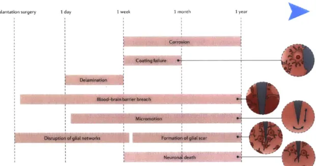
1.2 Development of neural engineering 1 year I r
A
F---7
I-~JzI
A'
Fig. 1.3: Failure modes of neural probes
Failure modes of neural probes have different origins and may become relevant at different times after implantation. Lifetime of neural probes can be increased by addressing these possible causes for device failure [Chen, Canales, and Anikeeva,
2017].
Implantation surgery I day I week I month
Corrosion
-
MicromotlonDisruption of gilal networks Formation of glial scar
1.2 Development of neural engineering
scar consists of reactive astrocytes and activated microglia forming an electrically inactive layer ( 100 pm thick) around the neural probe, thus preventing detection of any neuronal activity by the device [Kozai et al., 2015; Polikov et al., 20051 . Suggested causes for this inflammatory response include initial tissue damage dur-ing device insertion [Polikov et al., 2005; Ward et al., 2009], micromotion coupled with the elastic modulus mismatch between a neural probe and surrounding tissue [Barrese et al., 2013; Lee et al., 2005; Lind et al., 2013], breach of the blood-brain barrier [Saxena et al., 2013], disruption of glial networks [Seymour and Kipke, 2007], chemical mismatch between the implant surface and the cell membranes and extra-cellular matrix [Polikov et al., 2005], and neurotoxicity of the materials found in the device [Kotzar et al., 2002].
Damage due to device insertion has short-term effects on the performance of the probe, but the other failure modes impact the long-term performance, and so are of particular concern when designing a probe. It has been hypothesized that disrup-tion of local communicadisrup-tion between glia can occur when objects exceeding 20 pm are introduced into the brain. This in turn triggers the release of pro-inflammatory cytokines and the recruitment of additional activated microglia and reactive astro-cytes [Polikov et al., 2005; Szarowski et al., 2003]. The effects of the size of the device are also coupled to those of the elastic modulus, since smaller devices result in decreased bending stiffness. The implanted probes are usually tethered to the skull, and the elastic mismatch with the surroundings results in repeated injury to the tissue every time there is a displacement between the brain and the bone [Bar-rese et al., 2013; Lee et al., 2005; Lind et al., 2013]. This process has in turn been linked to a chronic breach of the blood-brain barrier (BBB) [Saxena et al., 2013],
1.2 Development of neural engineering
which activates glia and astrocytes to form a scar around the hemorrhage. In ad-dition to the mechanical properties of the probe, surface chemistry and topography may influence the extent of inflammation [Chapman et al., 20151.
Most neural probes are based on materials, such as silicon and metals, which have elastic moduli much higher than that of neural tissue (E 10s - 100s GPa vs.
E - kPa- MPa [Borschel et al., 2003; Gree et al., 2008]). However, it is the bending
stiffness, rather than the Young's modulus, that determines the tissue interaction with devices tethered to the skull or vertebrae [Chen, Canales, and Anikeeva, 2017]. The bending stiffness of a device is defined as the force that is required to achieve a certain deflection:
F 48EI
dL3 (1.1)
d LP
Here, F is the force, d is the deflection, E is the Young's modulus which is material dependent, I is the moment of inertia which is geometry dependent, and L is the length of the device. Equation 1.1 makes it clear that both, the geometry and the component materials of the device are important factors in determining its flexibility. In the case of a rectangular geometry, which is the most common geometry found in neural probes, the value for the moment of inertia can be substituted for this specific case:
F 4Ewt3 (1.2)
d P
where w and t are the width and thickness of the device, respectively. Equation 1.2 delineates the effects that the different dimensions of the probe have on its bending stiffness.
1.2 Development of neural engineering
This mismatch of the mechanical properties between the probes and the sur-rounding tissue may increase the likelihood of chronic tissue damage. In an attempt to reduce the stiffness of neural probes, different materials and design strategies have been implemented, including silk [Kim et al., 2010], polyimide [Takeuchi et al.,
2003], parylene C [Kuo et al., 2013], and silicone [Minev et al., 20151 substrates. Most of these devices, however, have planar geometries, and thus are more suited for recording from the surface on the brain than for reaching deep brain regions. Probes with a geometry similar to that of Michigan probes do have the ability to reach regions deep within the brain. However, fabricating long devices from wafers reduces the number of devices that can be produced simultaneously, significantly increasing the price of each probe. Thus, alternative methods capable of scalable production of neural probes are desirable.
In this work I aimed to design and fabricate neural probes that combine some of the most important requirements of a neural probe: (1) use of soft materials, along with minimal footprint to improve biocompatibility, (2) incorporation of sev-eral electrodes and multiple functionalities for bidirectional communication with the nervous system, (3) scalable fabrication methods. I also address one of the limitations of probes with fibrous geometries such as microwires, stereotrodes, and tetrodes, which is that they are not capable of depth dependent interaction with the surrounding tissue. For this purpose, I make use of a thermal drawing process
2 Fabrication Methods
2.1 Thermal drawing process
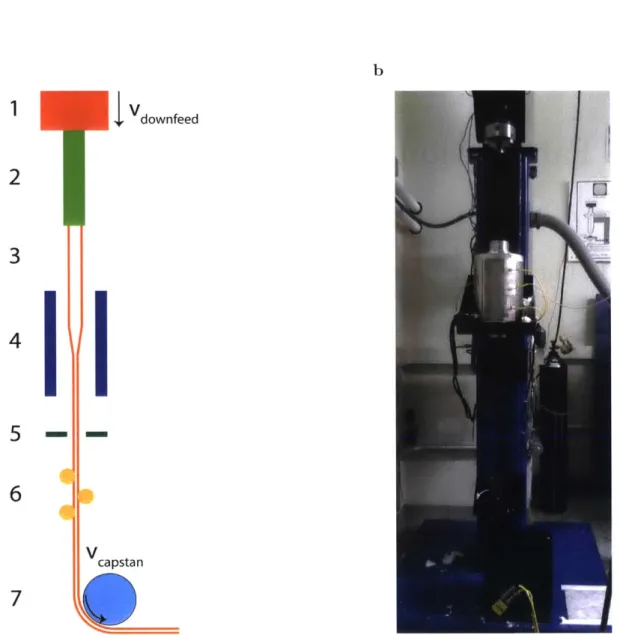
The thermal drawing process (TDP) has traditionally been used in the fab-rication of optical fibers [Goff and Hansen, 2002]. This fabfab-rication process starts with the fabrication of a preform, which is a macroscopic template of the fiber. The preform is then heated and stretched by applying controlled tensile stress [Tao et al.,
2012b] in a drawing tower (Fig. 2.1). This reduces the cross sectional features of
the preform by a reduction factor of up to 200 [Yaman et al., 2011], while increasing the preform length by the square of that factor, resulting in a fiber hundreds of meters long:
Reduction Factor = Lfbe _ Apreform (2.1)
Lpre form Afiber
where L and A represent the axial length and cross sectional area respectively.
The TDP has been used mainly to process glasses, however, this process can be applied to a variety of materials, including polymers, semiconductors and met-als, to fabricate multimaterial fibers [Abouraddy et al., 2007]. Although most of the applications of devices fabricated using the TDP are in optics, the ability to
2.1 Thermal drawing process
b
Fig. 2.1: Structure of the draw tower used during the TDP
(a) Schematic of the drawing tower showing the different parts composing it: (1) downfeed with controllable speed, (2) preform holder, (3) the preform
be-ing drawn, (4) furnace with 3 independent temperature control zones, (5) laser
micrometer, (6) tensiometer, and (7) capstan with speed control. Draw
condi-tions are affected by controlling the (1) downfeed speed, (4) furnace temperature
and (7) capstan speed. The drawing process can be monitored using the
(mi-crometer) and (tensiometer). (b) Picture of a drawing tower (1tof. Yoel Fink's group). a
I
Vdownfeed2
3
4
5-6
I
P
1
Vcapstan7
2.1 Thermal drawing process
combine multiple materials into a single fiber allows to fabricate functional devices for many different geometries and applications such as mechanosensors, chemical detectors and temperature probes [Abouraddy et al., 2006; Bayindir et al., 2006a,b; Chocat et al., 2012; Egusa et al., 2010; Fink et al., 1998; Gumennik et al., 2012; Kanik et al., 2014; Khudiyev et al., 2017; Shapira et al., 2006; Sorin et al., 2007; Stolyarov et al., 2012; Tao et al., 2012b]. There are, however, limitations on the properties of the materials that can be processed together, which must be taken into account during preform design. Furthermore, it is important to prepare the constituent materials before preform fabrication, such as cleaning them to prevent foreign objects from causing defects in both the preform and the resulting fiber. In the case of polymers, it is also vital to ensure that the materials are properly dried and degassed, since trapped solvents can evaporate and the gas expansion during heating results in bubbles which can deform the structure. This can be addressed
by baking the polymer at a temperature well below its glass transition temperature
under vacuum for a period of time which depends on the thickness of the sample and the actual temperature used, ranging from a few days for films tens of micrometers thick to several months for rods with a diameter of 4 cm.
When the preform is fabricated (Fig. 2.2a), all the geometrical features and material positioning of the final fiber are determined. This means that all functional components of the fiber can be designed and fabricated in a larger scale, usually in the millimeter to centimeter scale, before reaching its final, smaller size after the draw (Fig. 2.2b). There are several different methods that can be used during the preform fabrication [Tao et al., 2012b], including rod-in-tube approach, extrusion, stack-and-draw, thin film rolling, and fusing. In the rod-in-tube approach, a rod of
2.1 Thermal drawing process
one material is inserted in a tube of another material, resulting in a core-cladding structure [Ballato et al., 2008; Scott et al., 2009; Tyagi et al., 20101. Extrusion can be used to create multimaterial preforms, and is performed by heating the ele-ment materials of the preform above their softening temperature and pushing them through a die. The die determines the shape of the extruded preform, so that the cross section can be engineered to suit a specific purpose [Ebendorff-Heidepriem and Monro, 2007; Feng et al., 2005; Tao et al., 2012a]. The stack-and-draw method is widely used for fibers with small features. In this approach, multiple rods or tubes, consisting of either a single or of multiple materials, are assembled into a preform by holding them together inside a jacket [Canales et al., 2015; Liao et al.,
2009; Russell, 2003; Yaman et al., 2011]. This method is commonly used along
with recursive drawing steps to reach feature sizes down to the nanometer scale. A method uniquely suited for polymers, thin-film rolling uses flexible polymer films as the preform building blocks. These films are tightly rolled around a mandrel, which can be temporal or a rod of a material incorporated in the fiber. Heating the preform at a temperature above the glass transition temperature of the component materials consolidates all the films together, forming a solid cladding [Abouraddy et al., 2007; Canales et al., 2015]. In the fusing method, two parts of the preform, usually two slabs, are placed in a sandwich configuration and heated to fuse the two parts together. Pressure can be applied during this procedure to facilitate fusion. Additional materials can be incorporated into pockets machined into these slabs, so that after pressing, a single-piece preform is obtained [Gholipour et al., 2016; Koppes et al., 20161. All of these approaches are compatible with multimaterial drawings, and often two or more of these techniques are combined to fabricate a single preform.
2.1 Thermal drawing process
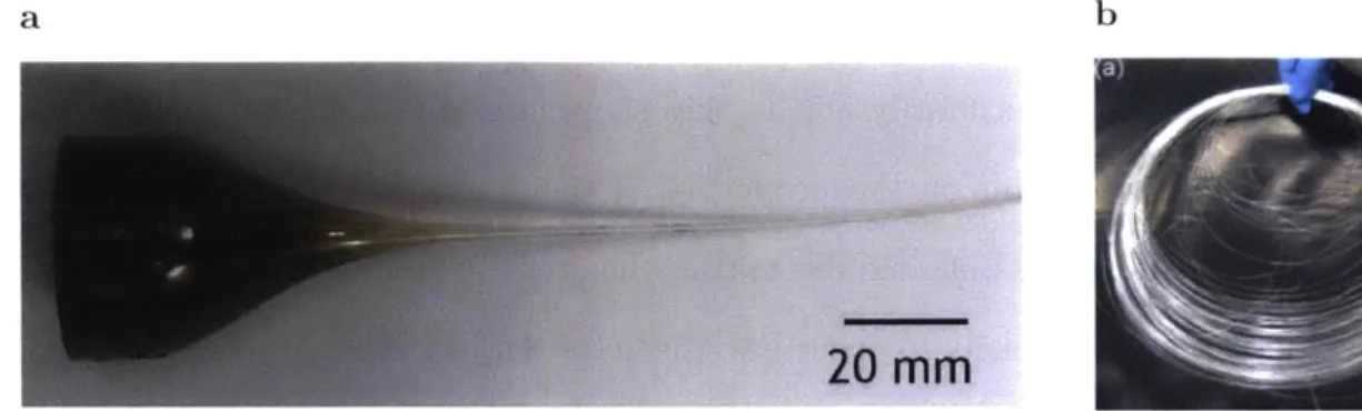
a b
20 MM
Fig. 2.2: Dimension scaling during thermal drawing process
(a) A picture showing the transition between preform and fiber occurring during
TDT. The cross section area decreases considerably during the process. (b) An example fiber obtained after thermal drawing. The length of the preform
( 20 cm) increases up to hundreds of meters of fiber, all preserving a
scaled-down version of the probe cross section geometry [Kanik et al., 2014].
When using multiple different materials in a preform, however, some require-ments must be met for the TDP to be possible [Abouraddy et al., 2006]. First, at least one of the materials must be able to support the stresses applied to the structure during the draw, and yet be continuously deformed in a controlled manner. Thus, a preform cannot consist entirely of crystalline materials, at least one of the materials must be amorphous. Also, crystalline materials must be enclosed in the preform by amorphous materials to preserve the preform structure [Tao et al., 2012b]. Second, all of the materials must flow at a common temperature at which the draw is carried out. The limit is usually set at a maximum viscosity of 10' poise for all materials [Chocat et al., 2012]. In the case of crystalline materials, their melting temperature must be below the drawing temperature. Finally, to ensure preservation of struc-ture and continuity of the individual materials in the fiber, materials must exhibit good adhesion/wetting in the viscous and solid phases without cracking even when cooled rapidly. Another aspect that needs to be taken into account during thermal drawing is the deformations that can be caused by capillary effects [Tomotika, 1935].
2.1 Thermal drawing process
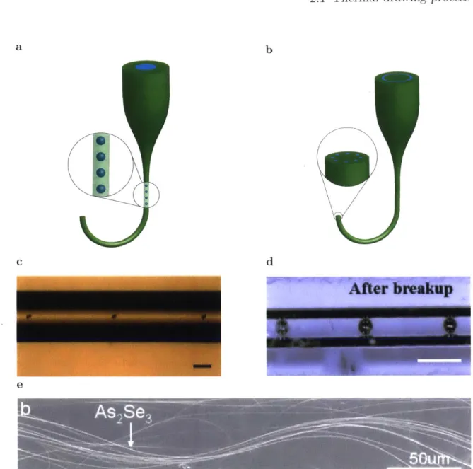
Capillary break-up primarily affects thin structures within the fiber, with the exact sizes being dependent on the properties of the materials and the processing conditions, and can occur both axially and in the cross section. The factors deter-mining when break-up is likely to occur have been the subject of in-depth theoretical studies [Deng et al., 2011]. Briefly, the break-up process is affected by the viscosity of the materials in the fiber and the thickness of each layer of different material. For any such settings, there will be a characteristic wavelength for which instability growth is the fastest. During thermal drawing, the thickness of the film decreases, and so does this characteristic wavelength. Along the axial direction (Fig. 2.3a), however, any perturbation which could lead to capillary break-up, is stretched as the fiber is drawn so that it no longer corresponds to the wavelength of maximal growth, damping the development of instabilities. There is no such process along the radial or angular directions (Fig. 2.3b), and therefore capillary break-up is primarily observed in the cross section of the fiber rather than along its length. This phenomenon, however, does not eliminate the possibility of having capillary break-up along the axial direction.
Instances where capillary break-up is not only not prevented, but is incorpo-rated into the fabrication process instead can be seen in both, the axial direction for the fabrication of micro- and nano-scale, core-shell, and Janus glass spheres
[Kauf-man et al., 2012], silicon microspheres and p-n junctions (Fig. 2.3c) [Gumennik et al., 2013J, protein-encapsulating polymer particles [Kaufman et al., 2013], and in-fiber optoelectronic components (Fig. 2.3d) [Wei et al., 2016], and in-plane to fabricate semiconductor nanofilaments with aspect ratios on the order of 106 (Fig.
2.1 Thermal drawing process
b
d
After breakup
e
Fig. 2.3: Capillary break-up modes in fibers
a Axial mode of capillary breakup of a core within a fiber results in evenly spaced
spheres. The diameter and spacing of the spheres is determined by the size of the core. b Thin ring structures in the preform can breakup to form filaments running along the fiber length. c Simultaneous breakup of two parallel silicon cores (one n-type and one p-type) was used to form in-fiber p-n junctions (50 [Im scale bar) [Gumennik et al., 2013]. d Optoelectronic devices were fabricated in-fiber by breaking up a germanium core in between two platinum electrodes. The spheres formed during break-up make contact with both electrodes (200 pm scale bar) [Wei et al., 20161. e In-plane capillary break-up was used to fabricate very high aspect ratio semiconductor filaments [Deng et al., 2009]
a
C
2.1 Thermal drawing process
2.3e) [Deng et al., 20091. However, in most instances capillary break-up is not
de-sired, and so it is important to choose the right temperature for the TDP. Lowering the temperature, therefore drawing with more viscous materials, is the most com-mon strategy used to prevent capillary break-up.
Furnaces used during thermal drawing may include several independently con-trolled temperature zones, which can be used to preheat the preform before it reaches the drawing point which takes place at the zone with the highest temperature and to allow the fiber being drawn a more gradual cooling process. Besides temperature, there are two other parameters that can be modified to affect the drawing process. These parameters are the feed speed, and the draw speed. The feed speed is the speed at which the preform is fed into the furnace, while the draw speed indicates the speed at which the fiber is pulled out of the furnace. By changing these two parameters, the reduction factor of the drawing process can be controlled. The reduction factor, which is the ratio of the linear dimension of a geometric feature in the preform to the dimension of the same feature in the fiber, along with the size of the original preform, determines the size of the fiber and of each functional element it incorporates. The theoretical reduction factor is calculated by assuming incompressibility of the materials within the preform. Since volume is assumed to be constant, the volume of the preform fed into the furnace during any given period of time must be equal to the volume of fiber drawn out of the furnace during the same time period:
ApreformVfeed = AfiberVdraw (2.2)
2.1 Thermal drawing process
root of the area, the expression for the reduction factor is obtained:
Reduction Factor = Apreform Vdraw (2.3)
Afiber Vfeed
Since volume is maintained, reduction of the cross sectional dimensions by a factor equal to the reduction factor means that the length of the preform is expanded by the square of this same factor.
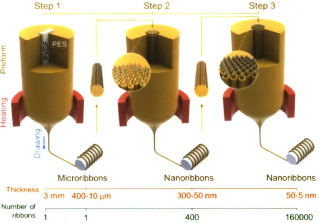
During thermal drawing, all features in the preform will be reduced accord-ing to the reduction factor. However, there are instances where features smaller than those obtained during the TDP are desired. One of the methods used to reach smaller features during fabrication is iterative thermal drawing [Yaman et al., 2011]. In this method, fibers obtained after a draw are used as building blocks of a second preform (Fig. 2.4). After drawing this new preform, the components present in the first fiber are reduced even further. Also, multiple fibers can be used in the construction of the second preform, increasing the number of components present in the new fiber. This process can be repeated multiple times, exponentially increasing the number of features in the fiber, and reducing the size of each component down to the nanometer scale [Kanik et al., 2014; Yaman et al., 20111.
Thermal drawing has been previously applied to fabricate neural probes (Fig.
2.5) [LeChasseur et al., 20111. In that work, the fabricated neural probe had a
struc-ture similar to that of optical fibers, but with an additional hollow core incorporated into the cladding. The materials used were the same ones used in the fabrication of
silica fibers. The hollow core was partially filled with an electrolyte, and a 50 Pm wire was inserted into it. Connection of this device to both a light source and a
2.1 Thermal drawing process
Step 3
Microribbons Nanorbbons Nanoribbons
Thickness Number of ribbons 3 mm 400-10 m 1 1 300-50 nm 400 50-5 nm 160000
Fig. 2.4: Iterative thermal drawing process
By using the fiber obtained from one drawing as a building block for a second
preform, the number of elements can be exponentially increased, while the size of each individual component is reduced even further each step [Kanik et al., 20141. Step 1 Step 2 0 w 0~ L F a: I
2.2 Lithographic fabrication
recording system, however, required a cross section area that was to big for chronic implantation into the rodent brain. To solve this challenge, one tip of the fiber was tapered by heating it and stretching it, in a process similar to thermal drawing, but at a smaller scale. After tapering, one of the tips of the fiber was sufficiently small to be inserted into the rat brain or spinal cord, while the other was large enough to allow access to an optical fiber connected to a light source and to the electrode in the hollow core. The electrode inserted in the hollow core was used to record electrical activity originating on neurons close to the fiber tip. This probe was therefore suitable for simultaneous optical stimulation and electrical recordings from neurons in the brain of anesthetized subjects. However, the connector for this device was bulky, and hence only allowed for short-term in vivo experiments in im-mobilized animals. Furthermore, the functionalities in this device were only active at the fiber tip, making the majority of the interface area between the device and the surrounding tissue unable to transmit any neural information. This limitation arises when using thermal drawing as the fabrication process since it is difficult to incorporate features along the fiber shaft.
2.2 Lithographic fabrication
Photolithography has been commonly used in the fabrication of neural probes. Having played a key role in the development of the semiconductor industry, it was used in the fabrication of the first silicon-based neural probes Campbell et al. [19911; Drake et al. [1988]. Despite the incorporation of new functionalities into the probes, and the use of softer materials in their fabrication, photolithography is still an im-portant part of the neural probe fabrication [Kim et al., 2012, 2013b; Rogers et al.,
2.2 Lithographic fabrication C Microprobe
d
Acquisition ... system Neutral density filter Dichroic Fiber mirror launch PMTLight insulation box Signal amplitude C .2 S-
..-b
Graded index optical core Hollow,..' core W * Excitation light a Fluorescencea Electric field potential
Fig. 2.5: Silica probe fabricated using thermal drawing
Figure showing schematics for (a) the neural probe, (b) preform cross section, (c) experiment design, and (d) modes of interaction between the probe and neural tissue LeChasseur et al. [2011].
a
UV-cura adh so-wire Multimode optical fiber light ble esive LM Graded index optical core Hollow core Shoulder Shank Tip2.2 Lithographic fabrication
2010; Rubehn et al., 20131. Using photolithographic methods allows straightfor-ward incorporation of functional components throughout the whole substrate sur-face. Most of these probes have a planar geometry, such as Michigan probes, but there are examples of probes with 3D structures [Kim et al., 2013a; Kuo et al., 2013; Takeuchi et al., 20031. Another advantage of this fabrication method is that it al-lows relatively easy interfaces for connection with recording systems. Components of the recording systems, usually connected to a computer, are fabricated using the same photolithographic methods, and several methods for connecting this type of components have been developed. However, probes fabricated on flat substrates via lithographic processes have limitations in the depth that they can reach, and are often associated with high production costs. The latter can be dramatically reduced
by parallel production, but this depends on the size of the device being small. The
introduction of larger wafers (up to 300 mm), helps to alleviate this problem. Larger wafers also allow for probes which are no longer limited by the depth they can reach inside the brain, but this in turn reduces the number of devices that can be pro-cessed in parallel.
Photolithographic processes [Moreau, 19881 rely on photosensitive polymers also known as photoresists. The solubility of these polymers changes after exposure to UV light due to changes in its chemical structure, or the degree of polymerization. This property allows to easily transfer complex patterns to films of these materials
by exposing them to light through a mask containing the desired pattern, and then
using a solvent to develop this pattern by removing either the polymer exposed to the light (positive photoresist) or the polymer left in the dark (negative photoresist,
2.2 Lithographic fabrication Negative Resist Mask UV source Expose Develop Positive Resist Resist Substrate
Fig. 2.6: Positive vs negative photoresist
When using negative photoresist, the polymer illuminated during exposure re-mains after the development step. In contrast, illuminated positive photoresist is removed during development.
way to controllably modify the structure of the fiber, especially along its shaft. In the case of neural probes fabricated using the TDP, it would provide a way to add functionalities throughout the entire length of the probe instead of being limited to
the tip.
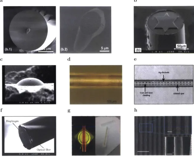
Efforts to combine thermal drawing with photopatterning have been made for different applications such as optics [Minh et al., 2003] and sensors [Abeysinghe
et al., 2002; Haga and Matsunaga, 2014] (Fig. 2.7). Photolithography has been used to modify the fiber tip [Abeysinghe et al., 2002; Minh et al., 2003; Sasaki et al.,
2002; Scheerlinck et al., 2009], and to generate structures surrounding a fiber [Fox
and Setter, 1996; Haga and Matsunaga, 2014; Hill et al., 1993; Katoh et al., 2001; Lu et al., 2010; Matsunaga et al., 2010] or even inside a fiber [Myr6n et al., 2004].
Lithography has also been used during the preform fabrication, to create metal nanowires [Gholipour et al., 2016] and to control fiber surface texture [Nguyen-Dang et al., 2017] after the thermal drawing. In none of these cases, however, the structure of the fiber itself, once drawn, is modified. Instead, additional materials
2.2 Lithographic fabrication
used to coat the fiber, either at the tip or along the shaft, are patterned.
Incorporating a photoresist into the preform structure would allow to pho-tolithographically modify the fiber structure directly. This would enable the incor-poration of functionalities, such as electrodes, along the length of the fiber. Also, it would facilitate connection to these functionalities, which is challenging with cur-rently available methods, especially in light of small features which require high spatial resolution. This type of connection could even allow for fiber-to-fiber con-nections, currently only done for waveguides, making it possible to have fiber-based complex devices without the need for intermediaries which are often necessary. Be-ing able to pattern the fiber would also allow to control its surface structure which has been shown to be useful in controlling the hydrophobicity of the fiber
[Khudiyev
et al., 2017] and to control cell growth [Koppes et al., 2016; Nguyen-Dang et al.,2017]. Furthermore, the incorporation of the photoresist to the fiber structure would
allow to achieve these modifications of fiber structure in a streamlined way. An ex-posure chamber could be used to pattern the fiber immediately following drawing as it is drawn, which could be an advantage when fabricating these structures in-dustrially.
2.2 Lithographic fabrication a b b50o m (b.2) bg c d e ML = _AM 7W 5 U 5.@ k V .4.5 iK .b, f g h Diaphragm Optical fiber
Fig. 2.7: Examples of, photolithography used in fiber substrates
(a) Gold grating fabricated in a fiber tip using transfer lithography. The resist
was UV-cured through the fiber core [Scheerlinck et al., 2009]. (b) Another example of patterning done on a fiber tip using a mold to transfer the pattern [Sasaki et al., 20021. (c) Microlens at the end of a fiber fabricated through dry etching using photoresist as a mask [Minh et al., 2003]. (d) Photoresist pattern after coating the fiber shaft and using a step-forward alignment method for photolithography [Lu et al., 2010]. (e) Silver electrode inside the hollow core of a fiber patterned using ablation [Myr6n et al., 2004]. (f) Example medical device fabricated using a combination of lithography techniques and fiber fabrication.
A SiO2 diaphragm at the tip of the fiber can be used as a pressure sensor in blood
vessels [Haga and Matsunaga, 2014]. (g) Lithographic techniques can also be incorporated during the preform fabrication. This image shows the patterning of gold deposited on glass. After the thermal drawing, gold nanowires are obtained [Gholipour et al., 2016]. (h) Hierarchical textures in the fiber were defined in the preform using molds fabricated using photolithography (scale bar: 100 pim; top right: 20 Am; bottom right: 1 Am) [Nguyen-Dang et al., 20171.
3 Design and fabrication of
fiber-based probes
In order to maximize the biocompatibility of our neural probes, polymers were selected as the main components to increase their flexibility and chemical compati-bility with neural tissues. The constraints of the thermal drawing process (TDP), in turn, restricted the options for additional materials that can be used in the device.
3.1 Multiwire arrays
This section is largely based on Canales et al. [2015].
The multiwire arrays were designed to have a multielectrode probe with high spatial resolution, aiming to be able to record from individual neurons in each elec-trode. Furthermore, these probes addressed the need for biocompatible probes by minimizing its bending stiffness through the choice of soft materials, such as poly-mers, and size reduction. Using a geometry inspired by tetrodes, I designed a multielectrode array in which the number of electrodes could be scaled up from the four found in tetrodes to several tens of electrodes while still maintaining a small footprint. For this device, materials with high conductivity, such as metals, are
3.1 Multiwire arrays desired for the electrodes, so that small wires can still be useful to record neural activity. Concomitantly, using polymers as the cladding of the device requires a ma-terial that has a low melting temperature (Tm). Tin (Sn), a metal with a melting temperature of 232 C, fulfills both of these requirements. Due to the requirements of TDP, the cladding of the probe must be a polymer with a glass transition tem-perature (Tg) similar to the Tm of tin. Polyetherimide (PEI, T9 = 215 'C) fulfilled this requirement, and so was used as the cladding material.
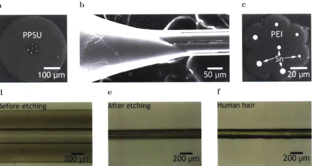
3.1.1 Thermal drawing process
The multiwire arrays were fabricated using a two-step TDP (Fig. 3.1b, e) that has been shown to be useful in producing arrays of semiconductor sub-micrometer wires [Yaman et al., 2011]. In preparation for the fabrication process, PEI rods were annealed in a vacuum oven at 150 C for -8 weeks to dry and prop-erly degas them. First, a hole 1/4" in diameter was drilled into a PEI rod 1.5" in diameter and 8" long, and subsequently filled with a tin rod (6 mm in diameter and 160 mm long). The resulting preform was drawn at 300 - 325 'C, resulting in tens of meters of a fiber 2 mm in diameter. The resulting fiber was then used to fabricate a second preform by using sections of the fiber to fill a hole drilled into a second polymer rod. After each step, the cross section geometry of the preform (Fig. 3.1a, d) was preserved, but at a smaller scale, in the fiber (Fig. 3.1c,
f). Using the iterative TDP allowed to scale up the number of tin electrodes to 36, while reducing their size down to 5.1 1.4 pm (mean t s.d.) and maintaining uniform spacing (23.3 + 1.5 pm).
3.1 Multiwire arrays ab c Heat d e PPSU 4Heat 1 00 pm
Fig. 3.1: Fabrication of multiwire arrays
(a) Initial preform for the first TDP step, consisting of a PEI cladding
surround-ing a tin core. After thermal drawsurround-ing (b), a (c) fiber with the same geometry of the initial preform, but at a smaller scale, is obtained, as shown by the SEM picture. Samples were prepared for imaging by embedding sections of the fiber in an epoxy matrix. After the epoxy was cured, the sample was polished using sandpaper of successively smaller particle sizes (120 to 4000 grit sizes, FEPA designation). The polished sample was imaged using a scanning electron mi-croscope (SEM, 6010LA, JEOL). (d) Several sections of the fiber obtained in the previous step were used to fabricate a second preform. Fiber sections are surrounded by a PPSU cladding. (e) Iterative thermal drawing allows to reduce feature sizes even further. (f) SEM of the fiber after the second TDP step. The
geometry of the preform is maintained, but scaled down. The final fiber has 7 tin
electrodes, each embedded in PEI cladding, and a PPSU cladding surrounding the whole device.
3.1 Multiwire arrays
3.1.2 Minimizing the footprint
Since my goal was to develop a neural probe with improved biocompatibility, one of the key designing factors was the final size of the probe. The cladding of the device, incorporated during the second drawing step, provides vital mechanical support during the fabrication process but serves no purpose following drawing. An alternative is to use a different polymer for the cladding of the second preform, so that it can be removed after the second drawing step. The chosen polymer must not only fulfill the previous requirement of having a glass transition similar to that of the other materials in the preform but also that provides a way to remove it without affecting the other components of the fiber. Polyphenylsulfone (PPSU, Tg =220 C) is compatible to be drawn together with both PEI and tin. Furthermore, PPSU is soluble in in tetrahydrofuran (THF) while PEI is not, thus providing a way to chemically remove the secondary cladding without affecting the rest of the fiber.
PPSU was treated in the same way as PEI, first annealing it at 150 C for ~8 weeks
and then drilling a hole (5/16") which was then filled with sections of the PEI/Sn fiber. The preform was then consolidated by heating it in a vacuum furnace at
253 C for 40 min, so that gaps left between the cladding of the fiber sections were
closed. After the TDP (Fig. 3.2a, d), the secondary PPSU cladding was removed
by immersing the fiber into THF for 25 min (Fig. 3.2b), resulting in a more flexible
fiber (Fig. 3.2e) with a size similar to that of a single human hair (Fig. 3.2c, c, f).
3.1.3 Increasing the number of electrodes
The iterative drawing process used for the fabrication of the multiwire arrays is uniquely suited to enable to increase the number of electrodes in the probe.