Aligned T-Gate Fabrication Using X-ray
Lithography
by
Mitchell Meinhold
B.S. Electrical Engineering, B.S. Engineering Physics Lehigh University (1994)
Submitted to the Department of Electrical Engineering and Computer Science in partial fulfillment of the requirements for the Degree of
Master of Science
in Electrical Engineering and Computer Science
at the
Massachusetts Institute of Technology
,0 Massachusetts Institute of Technology 1996. All rights reserved.
Signature of Author
Ddpartment of Eectrical Engineering and Computer Science 30 August 1996
Certified by
I,.
/
Henry I. SmithKeithley Professor of Electrical Engineering Thesis Supervisor
Accepted by ,
-Arthur C. Smith Chairman,. Departmental Committee on Graduate Students
MAR 0 6 1997
~:
.-Aligned T-Gate Fabrication Using X-ray Lithography
byMitchell Meinhold
Submitted to the Department of Electrical Engineering and Computer Science
on 25 September 1996 in partial fulfillment of the requirements for the Degree of Master of Science in Electrical and Computer Science.
Abstract
T-gate structures are employed in the construction of high performance MESFETs and HEMTs. A process using X-ray lithography and high precision alignment for the production of aligned, 0.1 ýtm T-gates has been developed. The constituents of layout design, mask fabrication, alignment and lithography are explored. The results of the experiments are presented and discussed.
Thesis Supervisor: Henry I. Smith
Acknowledgments
Because of the tremendous amount of aid and support that I have received from my professors and colleagues, this section may be as difficult to write as any other. First, I thank my advisor, Prof. Henry Smith not only for his guidance but for providing me with the opportunity to work in the Nano Structures Laboratory. I thank James Gooberlet for his generous time in writing masks, Isabel Yang for her help with optical mask preparation, and Euclid Moon for his help with the x-ray exposure & alignment system. I also thank Mike Lim, Dave Carter, Jim Carter, Tom Murphy and everyone else at NSL who have helped me with equipment and have generously shared their knowledge and know-how. Finally, I thank my family and friends who have been supportive and have motivated me throughout my career.
List of figures
Figure 1-1 T-gate cross-section with typical dimensions ... 7 Figure 1-2 Current technology for T-gate production using direct-write e-beam
lithography. The first step is an e-beam line exposure. The second step
demonstrates the unequal development rates of the resist layers forming the gate profile. Similar tri-level schemes are also used... 8 Figure 2-1 Three basic FET types: A) Si based JFET [6]. B) III-V based MESFET [2] C)
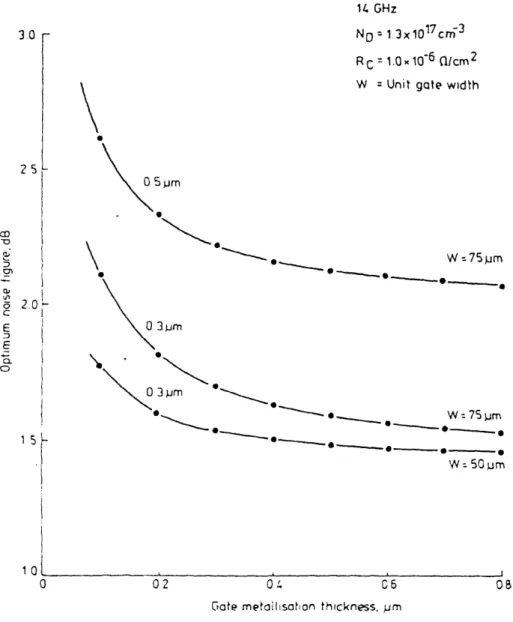
GaAs HEM T (or M ODFET) [2] ... I I Figure 2-2 Theoretical variation of optimum noise figure with gate metallization
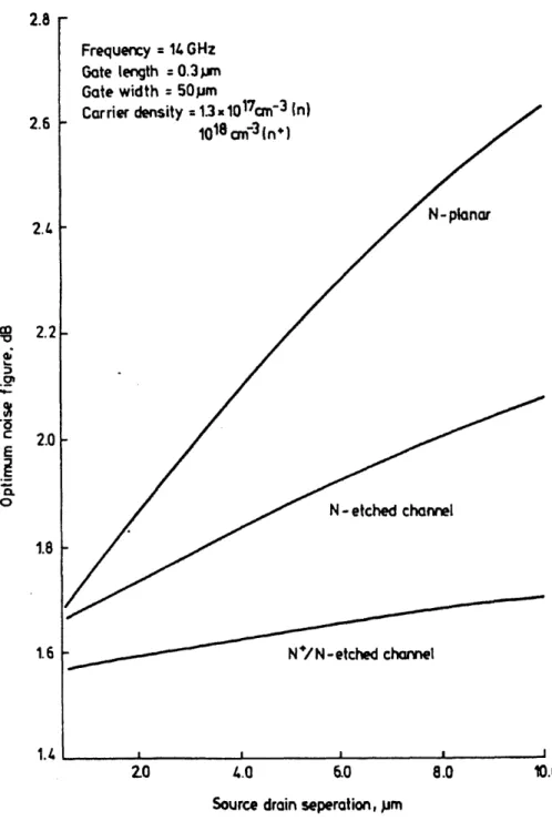
(vertical) thickness. Shows a 0.5dB drop in noise with a 0.2.tm decrease in gate length. Taken from DiLorenzo [2] ... 13 Figure 2-3 Variation of device optimum noise figure with source drain spacing. Taken
from DiLorenzo [2]... ... 14
Figure 3-1 Layout showing all three mask levels superimposed... 18 Figure 3-2 Diagram and cross-section of x-ray mask ... 19 Figure 3-3 CCD image of x-ray mask plating base etch taken from optical microscope. It
shows accelerated plating base etch in the vicinity of gold patterns. Separation between groups of "dots" is 100 p.m which is the field size. Etched circles actually encompass groups of four gold plated registration marks (see Figure 3-4) ... 20 Figure 3-4 Schematic of field with e-beam registration marks located at corners ... 22 Figure 3-5 Schematic of pattern transfer rig from optical mask to X-ray mask ... 22 Figure 3-6 SEM micrographs of gold plated, single pass lines which terminate at 500nm
boxes. Dose is varied from line to line. Lines with insufficient dose do not clear and do not fully electroplate... 24 Figure 3-7 Plots of linewidth vs. dose for: a) i= 50pA and start frequency of 240kHz. b)
i = 100pA and start frequency of 480kHz. c) combined a & b...25 Figure 3-8 Demonstration of moire effect. Pairs of gratings with different pitches are
located on the mask and wafer ... 28 Figure 3-9 A) 3-D view of alignment marks showing that grating with pitch P2 on mask is
matched to grating pi on wafer. The adjacent pair has p, on the mask and p2 on the wafer. B) Demonstration of fringe movement resulting from mask
Figure 3-10 Diagram of aligned marks. Alignment is achieved when fringes are matched.30
Figure 3-11 Full alignment mark set: Coarse alignment increases the capture range of alignment. Two full sets are placed on each mask so angular alignment can be d o n e ... 3 1
Figure 3-12 Depiction of alignment scheme used for x-ray mask alignment to wafer. Wafer alignment marks are "hatched" to improve diffracted light intensity. Since back diffraction is used, optics do not interfere with x-ray flux ... 32
Figure 3-13 CCD image of moir6 pattern produced from 5.6ptm pitch gratings ... 33
Figure 3-14 CCD image of moir6 pattern produced from 2ptm pitch gratings ... 3.... 33
Figure 4-1 Schematic of x-ray exposure system showing source, vacuum window, mask and sam ple (stage not shown) ... 34
Figure 4-2 SEM micrographs of un-protected SAL601 after x-ray exposure... 36
Figure 5-1 Diagram and optical microscope CCD photos of alignment state after exposure and development. The fringes are the result of the moir6 pattern
between the gold on the substrate and the pattern developed in the resist... 44
Figure 5-2 Measurements of gate stem alignment with respect to pads. The misalignment in a) is 118 Snm while in b) it is 12nm. The locations of these structures with respect to alignment marks are depicted as cc and 03 in Figure 3-1 corresponding to a) and b) respectively ... 47
Figure 5-3 Diagram of mask stage position control. Simultaneous control of both piezos translate the mask in the y-axis while differential control changes 0. ... 48
Figure 5-4 SEM micrograph of T-gate with 1 00nm footprint. The structure of the gate could be improved by increasing the height and straightness of the stem... 50
Figure 5-5 Dependence of linewidth on various process conditions for a negative
chemically amplified resist. (Taken from [1].)... 51
Figure 5-6 SEM micrographs of free-standing T-gates which vary in width. For gates wider than about 10 pm, uneven stress causes the gate ends to "curl up" as seen in g) and h). For larger gates, the effect can loosen the material entirely or cause the m etal to m eander, as seen in i)... 53
Contents
A bstract ...
2
L ist of Figures ...
...
4
1 Introduction ...
. ...
7
1. 1 Overview ... 92 M otivation ...
10
2.1 Introduction... 10 2.2 Transistor Types... 10 2.3 M ESFETs ... 12 2 .3 .1 N o ise ... :... 12 2.3.2 Frequency Limits ... 14 2.4 HEMTs ... 15 2.5 Summary ... 163 Layout and M ask Fabrication ...
17
3 .1 L ayo ut... ... 17
3 .2 M ask s... 18
3.3 E-beam Registration ... ... 21
3.3.1 Optical M ask for E-beam Registration M arks... 21
3.3.2 Optical Exposure of X-ray M asks ... 22
3.4 X-ray M ask Resolution... 23
3.5 Alignment M arks ... 26
4 Lithography ...
34
4.1 X-ray Source ... 34
4.2 Resist and W afer Preparation... 34
4.2.1 Chemically Amplified Resists ... 34
4.2.2 W afer preparation ... 36
4.3 Lithography Steps... 36
5 R esults and A nalysis ...
... 44
5.1 Alignment ... 44
5.2 Gate Quality ... 48
5.2.1 Stem Length, Aspect Ratio and Roughness ... 48
5.2.2 M echanical Stability ... 51
5.3 Summary ... 54
5.3.1 Future W ork ... 54
1 Introduction
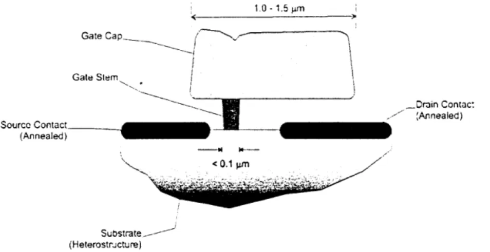
The growing industry of mobile and satellite communications equipment provides an ever increasing demand for field effect transistors (FETs) which can not only perform better, but can also be manufactured at a high throughput and low cost. While there are many issues to be dealt with in device design, one of the key hurdles is the fabrication of the gate and top level contacts. As will be detailed in the following chapter, device performance can be directly improved by reducing the resistance of the gate, allowing the transistor to be switched faster. The production of a T-shaped gate lowers gate resistance while keeping the channel length short. Low gate resistance and short channels boost the major figures of merit for this type of device. Such a gate with typical dimensions is shown in Figure 1-1. 1.0 - 1.5 pm Gate Cap_ Gate Stem Drain Contact (Annealed)Annealed) Source Contact• \•.•< <0.1 PMn Substrate- -(Heterostructure)
Figure I-1 T-gate cross-section with typical dimensions
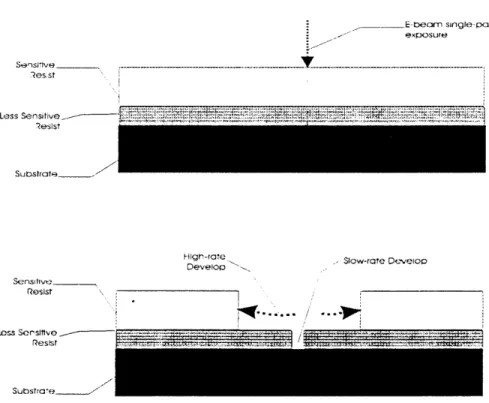
Conventional methods for T-gate fabrication are based on scanning electron beam lithography (SEBL) whereby patterns are written in a serial fashion [4,5]. In the case for T-gates, two or three resist layers of varying sensitivity are spun onto the substrate as depicted in Figure 1-2. The electron beam is then used to write a single line which provides an energy or charge dose to all resist layers. Since the layers may have different sensitivities though, the development rate may differ among the layers. By engineering the resist layers properly, a narrow line may be developed in the bottom layer while a much wider line is developed out of the upper layer. This forms the "cast" or mold for the
T-gate. Several shortcomings of this process should be noted. First, e-beam lithography does not allow for high throughput or large scale integration - at least not at a reasonable cost . Second, by its nature, the process will not easily yield asymmetrical gates which provide a degree of freedom for the designer. Third, control over device dimensions such as the stem width and aspect ratio may not remain under tight control since a slight variation in e-beam power conditions can alter the final results significantly.
" . E Dearn single pass exposure SensieIve-_. Zes'st Less Snsitiv ~.- I Less Sensitive-Resist Subslrater
Develop Slow-rate Develop
Sensitive
Res"st
Loess SerslItve Resist
Substra ee- ,
Figure 1-2 Current technology for T-gate production using direct-write e-beam lithography. The first step is an e-beam line exposure. The second step demonstrates the unequal development rates of the resist layers forming the gate profile. Similar tri-level schemes are also used.
Methods using tri-layer resist schemes in combination with deep-UV lithography have also been demonstrated [5]. In this case, however, a limit in linewidth (resolution) exists as well as a lack of control over relative positioning of stem, cap and contact edges.
Using aligned x-ray lithography (XRL) for the fabrication of FET gate structures offers several important advantages over the current technology. First, gate features are patterned in a sequence of two quick exposures as opposed to writing the patterns sequentially using an e-beam system. Second, gate caps can easily be deposited asymmetrically upon the stem providing greater design flexibility. Finally, once an x-ray
mask is made, feature dimensions are more rigidly defined than in other processes. For example, there is no need to optimize developers, an important step in tri-level, single exposure schemes [7].
1.1 Overview
In order to demonstrate these capabilities, an x-ray mask set has been created which patterns two levels of metal deposition. The first mask defines the source and drain contacts in addition to alignment marks to which the following masks align. The second stage consists of two masks containing the gate patterns. The second mask contains the gate stem features while the third contains the gate cap features.
The process implements a double layer resist scheme. A trench is created in the first layer which defines the gate stem. A second layer of resist is deposited over the first layer so that a second, larger trench, can be created above the first trench. The resulting "double trench" structure defines the T-gate.
Chapter 2 reviews briefly the engineering demands on gate structures for certain FETs. An understanding of how T-gates improve frequency cutoff and noise characteristics is provided. Chapter 3 covers the work necessary for the lithography including design of the layout and preparation of the masks. Chapter 4 discusses the lithography steps including resist, wafer preparation, exposure, alignment, liftoff, etc. Finally, Chapter 5 presents the latest results and proposes future work necessary to improve the process.
2 Motivation
2.1 Introduction
The aim of this chapter is to provide an understanding of why a need exists to develop a fast, reliable, and cost effective process for the fabrication of aligned T-gates. By reviewing the basic principles of various transistor types, and from a brief analysis of the basic equations which govern their operation, the importance of these gate structures will be revealed.
2.2 Transistor Types
Wireless communication, satellite data transfer, and various military applications such as radar, implement a class of circuits known as monolithic microwave integrated circuits (MMICs). These circuits perform a variety of microwave functions such as amplification, mixing, switching and phase shifting. The FETs used in such circuits fall into two categories, the metal semiconductor FET (MESFET) and the high electron mobility transistor (HEMT).' For many MMIC applications, it is necessary that these FETs must be produced with a high degree of precision and accuracy if the resulting chip is to remain within specification. In order to maintain chip yields in the range of several tens of percent, process tolerances must be kept down to several percent [6].
Figure 2-1 shows several FET cross sections. The topmost, the Si based JFET, is shown because many of its characteristics are reflected in the MESFET below it. The metal gate of the MESFET forms a Schottky barrier junction with the underlying
semiconductor material which is modulated by the gate voltage. The HEMT shown in Figure 2-1c modulates the carrier concentration of a two-dimensional electron gas (2DEG) formed beneath the gate at the interface of differently doped layers. These high speed, short channel devices are candidates for T-gate technology.
' Identifying a HEMT by name can be confusing because of various equivalent names (acronyms) it may have: modulation doped FET (MODFET), 2-dimensional electron gas FET (TEGFET) and selectively doped heterojunction transistor (SDHT).
SiO,
L )
Source (late Drain
a 1i I-M I N _ -_N, N-channel layer P type substrate P channel -Schottky contact Gate S",, - w Drain Rc <.L LL L>/<1> < Rs• Rs L a a, A a., 11t N - layer -- ohmic contacts
high resistance substrate
b) MESFET cross section
LSU Le Lo GaAs (N doped) \ Gate Source- ,Drn/ AlGat,-As
(N doped)
... ...
undoped
AIGa,,As spacer Semi-insulatingGaAs substrate 2 DEG
C) HEMT cross section
Figure 2-1 Three basic FET types: A) Si based JFET [61. B) III-V based MESFET [2] C) GaAs HEMT (or MODFET) [2].
a)
Long-gate Si JFET2.3 MESFETs
2.3.1 Noise
The noise of a FET depends on many factors including material quality at the substrate layer interface, gate length, gate metal loss and source resistance. The Ill-V based MESFET shown in Figure 2-1 depicts an etched channel FET. The following example will serve to demonstrate which geometrical factors affect noise so that the demands on the gate/contact lithography can be understood. The noise figure for the MESFET in Figure 2-1 (based on the dimensions in the figure) is described by [2]
F = 1
+ kf
L5 6 W 2+0.6W +0.6 +-I-a + & + (2.1)a) hL hL N\a1 a, Na,
where: Fo = noise factor
k = material quality factor (0.033) f = frequency of operation in GHz N = carrier density in 1016 cm3
W = unit gate width in mm
h = gate metalization thickness in microns L = gate length in microns
p = gate metal resistively in 10-6 Q-cm
R= specific contact resistance in 10-6 Q-cm
and a's and Ls,'s are dimensions shown in Figure 2-1.
First, notice that the noise factor, Fo, can be reduced by reducing gate length, L. Notice also that the denominators of the first two terms represent the cross-sectional area of the gate which is inversely proportional to the noise figure. These terms are a result of the fact that noise is proportional to input resistance (gate resistance). Figure 2-2, a plot of noise figure versus gate width for gates lengths of 0.3 and 0.5p.m, demonstrates the drop in noise from improved gate dimensions. Finally, note the third term which indicates that noise is proportional to the separation between gate and source. From a lithographic point of view, a T-gate design with an aligned stem directly addresses these engineering constraints. This is because the gate stem length (Figure 1-1) may be kept short while the cross-sectional area is increased by the cap layer. This type of design approach addresses
the first two constraints in noise reduction. Furthermore, the alignment capability of the
stem with respect to the source edge provides control over Lso, the third factor affecting performance. S pm 10 Sjim U 14 GHz N = 1. 3x1017cm- 3 RC = 1.0 x 10⁻⁶ (lcm2
W = Unit gate width
W=75pm *e - o •* 3 jmrn W: 75Sum W 50 Sm
101
U metaliso 0ate thckness m
Ga0te metaillsschon thickness, pm
Figure 2-2 Theoretical variation of optimum noise figure with
gate metallization (vertical) thickness. Shows a 0.5dB drop in noise with a 0.2ýmn decrease in gate length. Taken from DiLorenzo [21. 3.0 ^^ r * 'i:
2.6 2.4 c 2.2 a; C 2.0 E 0 o• 1.8 1.6 1.4 4.0 6.0 8.0 10.0
Source drain seperation, pm
Figure 2-3 Variation of device optimum noise figure with source drain spacing. Taken from DiLorenzo [2].
2.3.2 Frequency Limits
The frequency performance of a transistor can be described by two different
parameters: fT -the transition frequency at which current gain falls to unity, and f. - the
frequency at which power gain falls to unity (maximum frequency oscillation). The
1
---current cutoff frequency can be described simply as [6] f=
1
(2.2) 2.r where L1 + X/2 (2.3) VsatHere, v,, is the saturated value of the electron drift velocity and X is the extension of the space-charge layer into the gate-drain space2. t actually represents the net charging time
of the total depletion region and grows with increasing gate length. fr is not generally considered a figure of merit for a device when power gain is important. Instead, f,,, is the figure of interest and is proportional to fT. A crude equation, (short of network analysis), which expresses fn.,, is [6]
(2.4)
Sf,= f
fnia, - IT2
where R, is gate resistance, ro is the output resistance, and Icu is channel current. Here, there is not only an inverse dependence on LG but there is also an inverse dependence on RG. This is because power gain decreases with increasing input resistance which is mainly gate resistance. Since T-gate design simultaneously reduces both LG and RG, we see again that this design approach addresses electronic design issues from a lithographic
perspective.
2.4 HEMTs
The most apparent difference between HEMTs and MESFETs is that in a HEMT,
conduction between source and drain is confined to a very narrow region a fixed distance from the gate (Figure 2-1). HEMTs are important because of their very low noise figures.
- This value depends only on the channel doping density, built in gate contact voltage, and applied voltages to gate, drain and source.
While many examples of applying T-gates to HEMTs may be analyzed, this section will introduce only one.
There has been some evidence that the following equation for minimum noise figure applies as well to HEMTs as it does to FETs [6]:
CR•. + R• ,
NF I
1
+ 2eo (2.5)where C, is the gate-channel capacitance, gmo is the transconductance, Ri is channel resistance, R. is source resistance and R, is gate resistance. This equation says that noise increases with increasing gate resistance. In addition, the value of the gate-channel capacitance increases with gate length, LG, requiring once again that gate length be kept short.
2.5 Summary
This chapter has provided a brief overview of the operation and engineering problems associated with MESFETs and HEMTs. Implementing T-gates allows the designer to reduce gate length in addition to reducing gate resistance. It has been shown intuitively that these two changes simultaneously increase cutoff frequencies and lower noise; two very important figures of merit which today's applications strongly demand.
3 Layout and Mask Fabrication
The layout has been designed to enable measurements of placement, stability and quality of the gate and contact structures. The functionality of the various regions of the layout is discussed below.
3.1 Layout
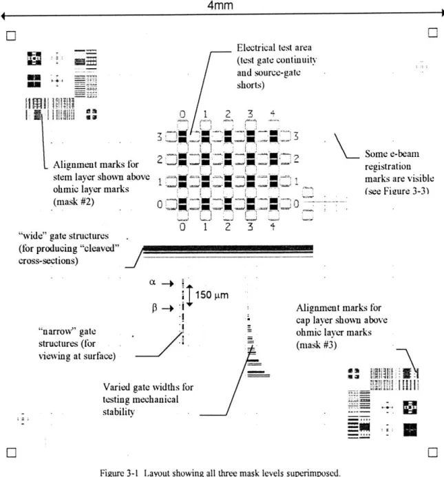
Figure 3-1 shows a view of the layout. In this figure, all three mask layers are shown superimposed. In order to evaluate the results of the T-gate process, the layout contains features which result in gate structures that can be examined in an SEM either in cross-section after cleaving, or top down as they appear on the substrate surface. The quality of the alignment and contact edges are determined in this manner by examining the position of the gate stem with respect to the source contact edge. In addition to this type of analysis, the layout contains source, drain and gate structures with adjoining 50p.m pads so gate continuity measurements and gate-source fault measurements are possible. Finally, it is possible to determine the mechanical strength and stability of the gates by examining unsupported gates of varying lengths and widths.
A
El
-"-as i
Alignment marks for stem layer shown above ohmic layer marks (mask #2)
"wide" gate structures (for producing "cleaved" cross-sections)
4mm
Electrical test area (test gate continuity and source-gate shorts) 0 1 2 3
0123
2 Ii Some e-beam registration marks are visible (see Fieure 3-3') I .J/
0 -4 "narrow" gate structures (for viewing at surface)Varied gate widths for testing mechanical stability
Alignment marks for cap layer shown above ohmic layer marks (mask #3)
-" ;i m
-m
Figure 3-1 Layout showing all three mask levels superimposed.
3.2 Masks
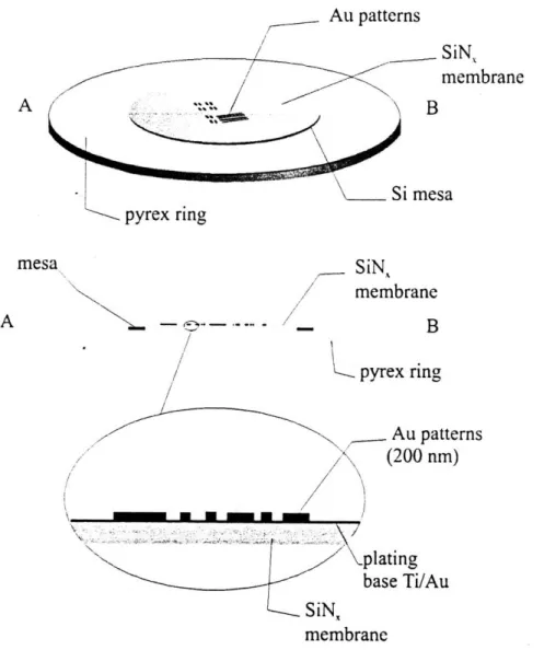
The masks are circular, l ltm-thick, SiNx membranes measuring 31mm in diameter. The Si "mesas" which support the membrane form a thin ring which is bonded to a Pyrex annulus. The masks are prepared with a plating base that is evaporated onto the membrane consisting of 100ooA Ti followed by 200A of Au. This step is followed by spinning 2200-2500A of PMMA and baking for 60min at 1800C. Patterning of the
ii·i; -* - i · 1 1 ·' i
-PMMN4A can be done either with deep UV (220nm) or by e-beam. Once exposed and developed, the resulting patterns become a cast for Au electroplating. The thickness of the PMMA determines the maximum height of the gold. For the x-ray wavelength used,
10dB attenuation is provided by 200nm thick Au. When the gold absorber is not thick enough, process latitude decreases because of poor contrast.
Au patterns / - SiN, A / Bmembrane Si mesa pyrex ring mesa A SiN membrane -• -... --
B
/
pyrex ring/
Au pa (200 n / " plating base Ti/A SiN, membrane tternsm)
uFigure 3-2 Diagram and cross-section of x-ray mask.
Once plated, the PMMA is stripped and 3-5.tm tall Al studs may be evaporated on the mesa in order to maintain a gap between the membrane and the sample during exposures. The gap, which reduces the chance of damage to the membrane, must be kept small (-5um) when exposing sub-1 00nm patterns.
The final step in mask preparation is the reduction or removal of plating base metal in the vicinity of the alignment marks. This is necessary because the light which is detected during alignment (see section 3.5) passes through the membrane twice. Since the
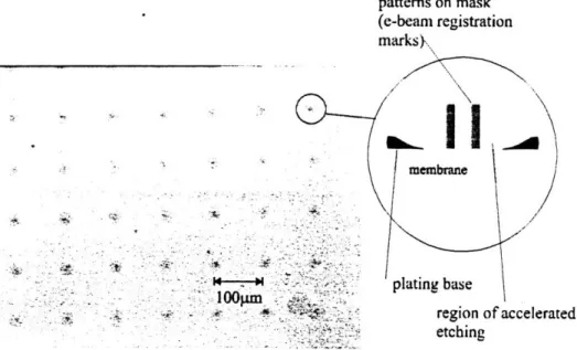
alignment marks are located about V2 mm from important features, it was possible to etch the gold plating base by pipetting a small droplet of Au etch solution directly onto the mask. A mixture of 10:1 DI water / Au etch solution was used for 2 minutes. Interestingly, the etch rate was accelerated at the edges of gold patterns. Figure 3-3 is an optical micrograph which shows this effect for the gold plated e-beam registration marks. It is speculated that this effect is the result of accelerated conduction in the vicinity of the gold aiding in the reaction which etches the plating base. Beyond 2.5 minutes of etching, patterns (such as crosses which were placed in registration mark optical mask described in the next two sections) begin to deteriorate. Beyond approximately 4.0 minutes, patterns apparently lose adhesion to the membrane and float away before their height is fully reduced. patterns on mask (e-beanm registration 10.n region of accelerated etching
Figure 3-3 CCD image of x-ray mask plating base etch taken from optical microscope. It shows accelerated plating base etch in the vicinity of gold patterns. Separation between groups of "dots" is 100pm which is the field size. Etched circles actually encompass groups of four gold plated
3.3 E-beam Registration
Mask fabrication must meet two challenges: precise and accurate overlay of the mask set and high resolution. To meet the first challenge, the mask set was written using a special registration. After placing a common grid pattern over the entire working area of each mask, features were written using this mutual reference system with a scanning electron beam lithography (SEBL) system. To meet the second challenge, tests were done to determine the optimal e-beam line dose for sub-1 00nm linewidths.
3.3.1 Optical Mask for E-beam Registration Marks
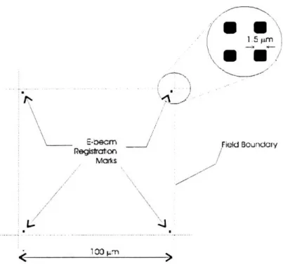
E-beam registration marks are first fabricated on a quartz optical mask. The registration grid consists of -I pm square dots placed near the corner of each 100Ptm X
S100Ptm field (Figure 3-4). This dotted grid was first produced optically using an optical pattern generator which exposed these marks over an area of one square die. (The final die size is 4mm.) This step resulted in a clear-field pattern on a glass emulsion mask at 10 times the final pattern size. The pattern was then "negated" (i.e., reversed to dark field) and then stepped down 10X using a g-line optical stepper onto a chrome coated quartz wafer having the same dimensions as an ordinary 4" Si wafer. With this pattern exposed and developed in photo-resist, the marks were then wet etched in the chrome.
I, E-beom Registraton Marks / 'g g
Jimu
Field Boundary / /.
. 100 .mrFigure 3-4 Schematic of field with e-beam registration marks
located at corners.
3.3.2 Optical Exposure of X-ray Masks
In order to transfer the optical mask grid pattern, close contact (-1 um) between the x-ray mask membrane and the quartz wafer was necessary. This was done by using a custom exposure mount which has been made for this procedure. It uses a gentle nitrogen gas flow which "pushes" the membrane up against the quartz mask during the exposure as shown in Figure 3-5.
DUV Radator (220rm)
chrome
N, In
-->na
X-raV S- \_N, Pressure Flow
(Quartz annulus)
X-ray
me:mane
Figure 3-5 Schematic of pattern transfer rig from optical mask to X-ray mask.
The exposures were done at a wavelength of 220nm for 15min. Once exposed, the x-ray mask is developed using a solution of 40:60 MIBK:IPA'. The mask was gold plated to about 1000
A
- half the possible thickness. With this amount of gold present on the mask, the SEBL system can track its relative beam position by scanning the grid marks prior to writing each field (Figure 3-4). It should be noted here that the grid may contain some degree of distortion since it is a product of optical projection lithography proceeded by optical pattern generation. However, the final placement of features is immune to this problem since the distortion is identical on all three x-ray masks.3.4 X-ray Mask Resolution
In order to determine final linewidth versus dose for single pass lines, a test pattern was produced which swept dose for both horizontal and vertical lines. Resulting lines terminate at 500nm boxes and join at corners as shown in Figure 3-6. The dose for each line is proportional to the beam current and inversely proportional to the speed of the beam. It is also multiplied.directly by the number of passes, n. Since the pattern is broken down into units of pixels measuring about 6nm, the speed of the beam, v, is dictated by the pixel clock frequency,
v = fxdI (3.1)
where dp is the pixel diameter and f is the clock frequency. Now the dose can be expressed as
dose
=
(
n
(3.3)
b
where I is the beam current, db is the beam diameter, and n is the number passes. Alternatively, the dose can be expressed without the beam diameter as
dose=( n . (3.3)
This equation expresses the dose as a line dose in units of nC/jpm and may better represent dose for single pass lines since the beam diameter is not well known.
The experimental results are shown in Figure 3-7 for a test mask with 2200A-thick PMMA. The dose is varied by changing the pixel clock frequency so that the lowest dose corresponds to a start frequency. As this frequency is decreased, the dose increases. Figure 3-7a shows the results based on a 50pA current and a starting pixel frequency of 240kHz. It is evident that the beam itself was asymmetric in the x and y directions since horizontal and vertical linewidths differ by about 10nm at the lowest doses. Below these doses, the lines were either broken or did not plate at all because the PMMA had not fully cleared. Increasing the beam current did not produce finer lines as seen in Figure 3-7c. Reducing the beam current below 50pA was not attempted because this would have made it difficult for the system to read registration marks thereby reducing the quality of positioning and overlay.
Figure 3-6 SEM micrographs of gold plated, single pass lines which terminate at 500nm boxes. Dose is varied from line to line. Lines with insufficient dose do not clear and do not fully electroplate.
Linewidth Vs. Dose Run 1: I = 50 pA 4 pass
I
___ I __ ___ __ .A~.. -t I (d~>. * I I I . Vert. Lines SHorz. Lines1.00E-04 2.00E-04 3.00E-04 4.00E-04 5.00E-04 6.00E-04
240kHz Dose (nCIlLm)
Run 1: I = 100 pA
Linewidth Vs. Dose 4 pass
41~
I I
* Series1 o : Series2 I
1 .00E-04 2.00E-04 3.00E-04 4.00E-04 5.00E-04 6.00E-04
480kHz Dose (nCIljm)
Run I & 2
Linewidth Vs. Dose
S50pA Vert. Lines 0 50pA Horz. Lines
A 100pA Vert. Lines
x 100pA Hor. Lines
1.00E-04 2.00E-04 3.00E-04 4.00E-04 5.00E-04 6.00E-04
Dose (nCl.m)
Figure 3-7 Plots of linewidth vs. dose for: a) i = 50pA and start frequency of 240kHz. b) i = 100pA and start frequency of 480kHz. c) combined a & b IE+00 eq. = 160.0 140.0 120.0 100.0 80.0 60.0 40.0 20.0 0.0 0.00 Start fri 180.0 160.0 140.0 120.0 100.0 80.0 60.0 40.0 20.0 0.0 0.00 Start fr )E+00 eq. = 180.0 1 160.0 140.0 120.0 100.0 80.0 60.0 40.0 20.0 0.0 0.0C)E+00
3.5 Alignment Marks
As shown in Figure 3-1, two alignment mark sets are placed at opposite corners of the die. In the first lithography step which defines the contact metal, the substrate receives marks at both corners. The mask for the gate stems contain marks only in the upper left corner while the mask for the gate caps contain marks only in the lower right corner. Since more than a single set of marks is needed for alignment of a particular mask, more than one die is written. Once the contact metal is deposited, the subsequent two exposures are each aligned to the substrate using a corner in turn.
The marks constitute a spatial-phase-matching system known as interferometric broad band imaging (IBBI). While the details may be found elsewhere [8, 10], a summary is provided here.
Figure 3-12 shows a diagram of the alignment system. The wafer sits on a precision stage which can be positioned in x, y, and azimuth angle 0. The mask is supported by a separate stage which has three symmetric arms extending outward from the center. Motorized actuators can move each arm independently or in union so that the mask can be made level to wafer. The mask stage also has piezo control for x and y axis alignment.
Coarse alignment is accomplished using a microscope to center cross and box alignment marks (as seen in the corners of Figure 3-1). Once coarse alignment is complete, the precision marks can be used. It will be shown that this coarse alignment step is very important because it removes the ambiguity of a full period phase shift when implementing the fine-alignment gratings.
The precision alignment marks, (shown in Figure 3-8), consist of gratings which overlay one another on the mask and the wafer. If the pitch of the wafer grating, pi, is different than the pitch of the mask grating, p2, then a beat pattern (or moir6 pattern) will be created having a pitch given by
PI P2
Pmoirc - (3.4)
Furthermore, if the mask is moved incrementally by a distance 6
mak, the displacement of the fringes is
Ps
jnges-
PA
2ask
(3.5)
1 - P2
This means that if 2ýtm gratings are used with a difference in pitch of 0.2p•tm, a 10x "amplification" in position is produced. The mask is designed with two sets of these gratings side by side as shown in Figure 3-9A. By switching pi and p2 for the adjacent set (meaning p, is now on the mask), a property of equation (3.5) is utilized: the direction of a fringe displacement of the second set of gratings will be opposite to that of the first set for a given displacement of the mask. That is, fringes shift in opposite directions. This motion is shown in Figure 3-9B. This effect amplifies the sensitivity of the alignment. The condition for alignment, shown in Figure 3-10, is achieved by ensuring that pair of fringes line up. This condition will be met, however, every time there is a relative mask
displacement of (p, + p2)/ 2. Therefore, coarse alignment must align to below the pitch of
(on wafer) (on mask)
Ii Pm
p, on top
of p,
Figure 3-8 Demonstration of moir6 effect. Pairs of gratings with different pitches are located on the mask and wafer.
A 3-Dimensional View mask grating p 1 9 P, p: .... wafer grating Top-down view
fringe =rmn
+ir
_j
ingee movement
movement Relative motion of mask
with respect to wafer.
Figure 3-9 A) 3-D view of alignment marks showing that grating with pitch p2 on mask is matched to grating pl on wafer. The adjacent pair has pl on the mask and p2 on the wafer. B) Demonstration of fringe movement resulting from mask displacement relative to substrate.
/
fringes are aligned
Figure 3-10 Diagram of aligned marks. Alignment is achieved when fringes are matched.
A full alignment mark set is shown in Figure 3-11. It includes two pairs of marks: one pair is for y-axis alignment while the other pair is for x-axis alignment. By including a larger pitch mark for each axis, the capture range of alignment is increased. Furthermore, by having two marks with different pitches, confidence in alignment is greater when fringes on both marks are aligned.
fine alignment in x-axis
Full I I
IlIlIllIlIll
I
NH
OH
lH
HI
lIlIlIllIlIlI
- - . fine alignenment in y-axis ~- - coarse alignment in y-axis immla~ coarse alignment in x-axisFigure 3-11 Full aligmnment mark set: Coarse alignment increases the capture range of alignment. Two full sets are placed on each mask so angular alignment can be done.
The gratings on the wafer are segmented (or hatched) as shown in Figure 3-12. When illuminated by the light source, the hatched period provides a back diffraction signal which occurs at about 80 from the z-axis. This allows alignment to continue during exposure since the optics will not interfere with the incoming x-ray flux. Although this light is back-diffracted by the wafer grating, it contains the moire alignment information. This image is projected onto a CCD camera which can provide the digitized information to a computer. An image processing algorithm can optimize alignment using Fourier transform techniques. In this experiment, however, alignment was done "by eye" as the auto-align was inoperative. Figure 3-13 and Figure 3-14 show the resulting images of aligned gratings for pitches of 5 and 2ptm respectively.
j !
°
/ P, P
Mask Alignment Marks
Laser input
X-ray flux Lens
I
/
Spliter CCD Camera I x-ray mask 'VV V V~ saple/wafer sample/wafer Wafer Alignment / Marks ->(Figure 3-12 Depiction of alignment scheme used fibr x-ray mask alignment to wafer. Wafer alignment marks are "hatched" to improve diffracted light intensity. Since back diffraction is used, optics do not interfere with x-ray flux.
Figure 3-13 CCD pitch gratings.
image of moird pattern produced from 5.6tim
Figure 3-14 CCI) image of moir6 pattern produced from 2im pitch gratings.
4 Lithography
4.1 X-ray Source
The ray lithography system used is a 1:1 proximity shadow-cast process. The x-ray point source is a water cooled electron-bombardment Cu anode operated at 8keV with an anode current of 75mA. Figure 4-1 summarizes the setup used in the Nano Structures Laboratory at MIT. A 1.7.tm-thick SiNx membrane is used as a low attenuation x-ray window in addition to maintaining the anode vacuum.
filunent SiN. vact . . window V (Helihunm ambnient) SiN. mask membrane -annode (wa -___Cu tip S (vacuunm) x-ray flux mask support "sample/wafer
Figure 4-1 Schematic of x-ray exposure system showing source, vacuum window, mask and sample (stage not shown).
4.2 Resist and Wafer Preparation
4.2.1 Chemically Amplified Resists
Chemically amplified resists, (CARs), consist of three components: a novolak binder matrix, a photo-acid-generator (PAG), and an acid catalyzed converter [12]. CAR exposures are a two step process consisting of exposure to e-beam or photons followed by a post-exposure-bake (PEB). During exposures, the PAG reacts with the incoming
ter cooled)
electron path
pyrex nng
electrons or photons to produce free acids. In the case of negative tone CARs, these acids catalyze the converter which crosslinks the novolak matrix. This second reaction requires a higher activation energy which is supplied during the PEB. Amplification occurs because the activation energy of the crosslinking reaction is provided by the PEB, not the exposure itself, and the acid is freed to produce additional crosslinks.
The time and temperature of the PEB are critical parameters in controlling the quality of final resist features. Vacuum hotplates are used for pre- and postbaking, allowing temperature control to within 1 degree C and repeatability to within 0.5 degree C.' During the PEB, the motion of the acids produced from the exposure is modeled as a random walk, where acids drift from areas of high concentration to areas of low concentration [3]. Fedynyshyn has shown that linewidths of several CARs expand as the square root of PEB time. Temperature also plays an important role in the quality of features since the best results are confined to a range of several degrees. Aside from PEB conditions, the need for a high contrast mask and small gap is important (see section 3.2).
Shipley SAL601-ER7 , a negative tone e-beam CAR, has been used for all lithography steps. This type of resist has several advantages over PMMA when used for x-ray lithography. First, since it requires a fraction of the dose that PMMA requires, exposure times for SAL601 tend to be about 4 times shorter. Second, since it is a negative tone resist, x-ray masks do not have to be replicated (daughtered) for use with this resist. This is because an x-ray mask which is written by e-beam is inherently clear field and usually requires daughtering (conversion to dark field) before useful patterns can be transferred to positive resists.2 This daughtering process, although being developed further, seems to have certain problems associated with it. Transfer of fine lines, (below 1 00nm), requires that the mask membranes come into full contact. This is done by pulling a vacuum between the membranes. Particles, stress and other factors must be minimized to reduce the possibility of mask damage or breakage.
This repeatablity assumes that the hotplate is not "loaded down", i.e., the plate temperature is allowed to stabilize before a new wafer is baked.
2 Processes carried out on substrate can implement clear field masks with positive resists by using resist lines as RIE etch masks to define features such as p6ly-Si gates.
4.2.2 Wafer preparation
X-ray exposures subject the resist to low energy photo-electrons which are produced by the interaction of the x-ray flux and the gold patterns on the mask. Without protection, the topmost region of resist becomes exposed, resulting in a hardened skin as seen in Figure 4-2. Since the resist is electron sensitive, a protective layer of PVA is spun over the resist to shield these electrons. Because PVA is water soluble, it is easily stripped from the wafer after exposure.
Figure 4-2 SEM micrographs of un-protected SAI,601 after x-ray exposure.
4.3 Lithography Steps
The following sequence describes a complete process for the gate lithography:
1. Dip Si wafer in dilute HF solution to remove native oxide and promote resist adhesion. 2. Spin SAL601 to a thickness of 700nm.
4. Spin 200nm of filtered PVA.3
200nm filtered PVA
700nm negative-tone resist (SAL601)
\ Si wafer
5. X-ray expose first mask (contact patterns including alignment marks). Currently, the exposure system is set to 27cm anode-wafer distance, 75mA anode current, and 8kV filament voltage. The exposure time chosen was 9 hours. Oxygen concentration in the He between the vacuum window and the wafer is kept below 200ppm.
,alignment /grating
contatts x-ray flux
cottt mask Au absorber -7um gap V V VT' Yr 200nm filtered PVA 700nm negative-tone resist (SAL601) Si wafer
' Spinning PVA can be difficult because it does not easily coat the wafer during acceleration. This problem was overcome by putting 5-10 ml ofpre-filtered solution into a 15ml beaker, pouring it onto the wafer, and beginning with a very low spin speed to achieve total wafer coverage.
'··'·1li·ll
6. Strip PVA with DI water and develop resist in 50:50 DI:Microposit MF312 developer for 2-2.5 min. contacts 700ra negative-tone S resist (SAL601) \ Si wafer
7. Evaporate contact metal, 10 Onm Ti, 200nm Au.
alignment grating contacts * I' 700nrn negative-tone resist (SAL601) 10nm Ti Si wafer
(* exaggerated aspect ratio) alignment grating
111111111111
1•
0ii:i/•
200nm Au 1 : . .1 ..ý lil f :"" II1II1 Ii ( i ll• .f ::•S'••.:'8. Liftoff. 200nm Au alignment grating contact \- 10Onm Ti \Si wafer
9. Spin 200nm SAL601. Prebake 900C for 1 minute. Spin 200nm of filtered PVA. 200nm PVA 200nm negative resist 7-',f 200nm Au 10nm Ti iSi wafer
10. Align second x-ray mask (gate stem patterns) to contact metal layer. Expose for
9 hours. Post bake at 1060C for 32sec.
alignment takes place x-ray flux stem feature (100nm) mask IInllnlllll V .- •-, 200nm PVA 200am negative resist 200nm Au 10\ Inm Ti Si wafer
11. Strip PVA with DI water and develop resist in 50:50 DI:MF312 for 20 sec.
Lr•2t ste'mf.... 200nm negative resist 200am Au 10am Ti ---IF ---IF ---IF I ~tF~P~Ld~W`n~alM~ i ~ ý, I n- - -r-
i
12. Harden resist by baking at I100C for 60sec. Spin second layer resist, 700nm
SAL601. Spin 200nm PVA.
S200nm PVA
2n layer resist (700nm)
I" layer resist n00( lm)i
200nm Au
S10nm Ti
Si wafer
13. Align third x-ray mask (gate cap patterns) to contact metal layer. Expose for 9 hours. Post bake at 1070C for 35sec.
aligrunent takes place
using second alignment
/ grating
~7um gap
V V V V v V V v7
I". layer resist
S (20Ohm) 200nm Au 10nm Ti Si wafer x-ray flux ooIann1un _200nm PVA\ 2' lavcr resist (700nm) I --~---I ~ ~4 · I ,Ig I I r II I r 1~
14. Strip PVA with DI water and develop resist in 50:50 DI:MF312 for 60-90 sec. S2" layer resist (-700nm) 1" layer resist L (-200nm) 200nm Au 10nm Ti Si wafer
15. Descum surfaces in 2% 02 plasma, 200W power for 10 sec. Deposit 10 nm Ti, 250nm Au gate metal. 250nm Au gate metal
/
10nm Ti 2d layer resist (-700nm) l' layer resist (-200nm) 200nm Au 10nm Ti Si wafer \ \ I !"" -o ý\j
16. Liftoff in 950C NMP, about 15min. Surface descum 2% 02 plasma, 200W power for 3min. 2_ 50nm Au gate metal S______ _O10nm Ti > \ 200nm Au S10nm Ti Si wafer
5 Results and Analysis
Results were inspected using an SEM after gate metal liftoff was done. The following sections evaluate the success of the alignment and the quality of the T-gate structures.
5.1 Alignment
Figure 5-1 shows a diagram of the relative positions of the alignment marks and the patterns after the gate stem exposure took place.
optically aligned marks T -2000!aml I
A/
-t-I "N patterns 4500,urn -2000prn 0 M C 0 8200psmFigure 5-1 Diagram and optical microscope CCD photos of alignment state after exposure and development. The fringes are the result of the moir6 pattern between the gold on the substrate and the pattern developed in the resist.
yA x
I
-,A
The alignment system was set up with a microscope to do course alignment prior to the fringe alignment. The algorithm used for alignment was as follows (based on Figure 5-1):
* Level mask.'
* Course align mask using wafer stage to bring features within 1 001Lm and perform a course adjustment of wafer stage 0.
+ ** Align cross and boxes optically (at B) using wafer stage x-y controls.
* Adjust wafer stage 6 (at A) so that:
Cross and boxes are fully aligned for the first few iterations.
Cross and boxes are halfway aligned for the following iterations.
-Ad f 6 C h d b hlf li d
W JU•L wa eL sta~ e •iat t.) so Lt aL rUsiu al Ul s are a way a ••e.; * Align y-axis moir6 (at A) using mask piezo control.
* Align y-axis moir6 (at B) using mask piezo control. * Align x-axis moir6 (at A) using mask piezo control. * Align x-axis moir6 (at B) using mask piezo control.
* Perform final y-axis moir6 alignment (at B) using mask piezo control as the mask is lowered into contact.
The results of this alignment were studied based on the moir6 fringes created between the developed resist and the gold patterns beneath them. The optical microscope CCD photos shown in Figure 5-1 contain this information which is summarized in the following table.
A B
x-axis misalignment y-axis misalignment
0.9 ± 0.1 gm (from ml) 0.08 ± 0.01 pm (fromm 2)
not detectable
not detectable
The x-axis misalignment detected at A suggests that 0 is misaligned by
Leveling the mask seems to reduce the gap at which the first stud touches the wafer. This allows alignment to be adjusted at smaller gaps. In order to retain alignment as the mask is set into contact with the wafer, the mask must be level.
0.2 ± 0.04 mrad. The y-axis misalignment detected at A suggests either that the mask has stretched between 50 and 80p.m or that there is some error associated in reading these small scale fringe shifts. Nonetheless, the outstanding misalignment in this experiment is angular misalignment. This is because the pattern misalignment resulting from an error of 0.2 mrad and a lever arm of up to 2000p.m is 0.4 p.m. Figure 5-2 contains two SEM micrographs of T-gates produced from this alignment. The location of these gates on the die is depicted as cc and
13
in Figure 3-1 corresponding to the top and bottom photos in Figure 5-2 respectively. It is surprising that up to 100nm of misalignment can be detectedfor gates with large pad separations (>2ptm) while only -20nm of misalignment is detected for smaller separations (<2p.m). While the magnitude of the detected misalignment in these SEM micrographs is significantly less than the 0.4 p.m calculated above, the direction is consistent with the angular misalignment detected from the fringes. This direction is a negative rotation (counterclockwise) of the mask about a pivot point in the vicinity of the alignment mark labeled A in Figure 5-1.
One solution to the problem of angular misalignment would be to place alignment marks on a diagonal rather than allowing them to be collinear in one of the alignment axes. Another solution would be to align 0 using the x-axis moir6 marks. The piezo system used to translate the mask in the y-axis is actually divided into two actuators as shown in Figure 5-3. By actuating each piezo in opposite directions, motion in 0 is achieved. The current problem is that only one mark can be "viewed" at a given time. This makes it difficult to adjust 0 while simultaneously maintaining alignment in x and y for both sets of marks. Therefore, it is likely that the best solution is to "squeeze in" two sets of optics and monitor both marks simultaneously.
Figure 5-2 Measurements of gate stem alignment with respect to pads. The misalignment in a) is 1 I8nm while in b) it is 12nm. The locations of these structures with respect to alignment marks are depicted as ac and 03 in Figure 3-1 corresponding to a) and b) respectively.
Y-axis mask control.
~-' V
P ICUIJ4d& bL46V 6,VIUUL
Figure 5-3 Diagram of mask stage position control.
Simultaneous control of both piezos translate the mask in the y-axis while differential control changes 0.
5.2 Gate Quality
5.2.1
Stem Length, Aspect Ratio and Roughness
The quality of the stem needs to be improved in order for these gates to be realized
in actual devices. Figure
5-4
is an SEM micrograph of a gate produced in this experiment.
Clearly, the stem height and straightness are not sufficient. Given a fixed exposure time of
9 hours, the 1
00rnm lines were produced by spinning only a 220nm film of resist, reducing
the PEB temperature to 106
0C and reducing the PEB time to 32sec.
2The difficulty in
resolution of the gate stems seems to surface when the lines are below 150nm in length.
Two theories which can explain this problem are as follows:
* The mask absorber thickness (or density) is insufficient resulting in too much
exposure in the trenches (not enough contrast).
2 The original parameters used were I 10*C and 60sec.
* The resolution of the resist is suffering at small linewidths because of the chemistry of the resist. The acids responsible for catalyzing the crosslinking process are diffusing into the stem, effectively exposing the resist in the trench.
If the first theory is true, it is not clear why slightly larger linewidths are attainable. AFM scans of the gate level masks indicate that the gold absorber height is only about 150nm. This absorber height is sufficient to produce >1 50nm lines (trenches). It may be that contrast plays a key role in determining the smoothness of pattern edges. If the scale of edge roughness is on the order of 100nm, then it may be that only lines below 150nm are poor because of this problem.
The second theory focuses on the parameters which affect the linewidth and appearance of the resist profile. For a negative chemically amplified resist, these parameters include dose, PEB temperature, PEB time, development time and developer concentration. Figure 5-5 is a table containing data for linewidth dependence of process parameters for a negative chemically amplified resist [1]. It is interesting to see that for this particular resist, a 9% increase in PEB temperature results in a 65% increase in linewidth, an increase in PEB time from 40 to 120 seconds doubles linewidth, and a 40% increase in dose (from 40 to 55 mJ/cm2) increases linewidth by 25%. Results like this seem to indicate that factors which affect the redistribution of the acid are significant in determining final resolution and quality. The strongest factor appears to be PEB temperature because of its exponential dependence. Therefore, achieving higher quality T-gate stems may be a matter of reducing PEB temperature while allowing the dose and/or PEB time to increase.
= ~ #1
r
-w S
r ~ ~~;r
Figure 5-4 SEM micrograph of T-gate with 100nm footprint. The structure of the gate could be improved by increasing the heiht and straightness of the stem.
XP-90104C lincwidth change vs. process conditions
Variable Value Linewidth (pmn) Appeanrance Dose 35 0.21-0.25 slight bridging
(mJ/cm 2) 40 0.30-0.35 OK
45 0.30 OK
50 0.39 OK
55 0.38 OK
PEB temp 104 NA lines eroded away
(C) 110 0.30 OK
116.5 0.46 slight bridging 119.5 0.50 slight bridging
PEB time 40 0.20 erosion and bridging
(sec.) 50 0.2--0.27 OK 60 0.30 OK 75 0.32 OK 90 0.35 OK 120 0.12 OK Dev. time 2.5 0.30 OK (min.) 30.30 OK (4 .26-0.28 OK Dev. conc. 0.2413 33 OK N).256 (.3 1.32 OK 0.27 0.( 3) OK 0.283 0).7 O)K 0.297 0.23 vr lightly undercut
Figure 5-5 Dependence of linewidth on various process conditions for a negative chemically amplified resist. (Taken from [1].)
5.2.2 Mechanical Stability
Some of the gates were fabricated without pad or block attachments. Figure 5-6
shows SEM micrographs of a number of these unsupported T-gates which have varying widths ranging from 1 to 50.tm. It was observed that for intermediate widths of 10 to
30Lm, the gate metal "curled upward" near the tips presumably due to uneven stress formed after the metal evaporation (Figure 5-6 g,h). Pinning the gate down at its ends or adding supports along its width seems to ensure that the metal does not detach, even for arbitrarily wide gate structures (such as the cleavable strips). Improving the quality of the resist profile which defines the stem may help make the gate adhere better to the substrate.
W= Lim a W = 2.25 Pm
W = I I II - '2 4..
W= I5um 2 W=7ium h W > 251m
Figure 5-6 SEM micrographs of free-standing T-gates which vary in width. For gates wider than about 10 pm, uneven stress causes the gate ends to "curl up" as seen in g) and h). For larger gates, the effect can loosen the material entirely or cause the metal to meander, as seen in i).
- I
5.3 Summary
A process for T-gate fabrication suitable for MESFET and HEMT devices has been explored. This double-layer resist process primarily takes advantage of two technologies: a high precision alignment scheme and proximity gap x-ray lithography. Gates with 100nm footprints and alignment to within approximately 100nm were fabricated. It was found that the misalignment of the gate stems was mainly the result of a lack of angular alignment. Solutions to this problem as well as methods to improve the quality of the gate stems have been proposed. Additionally, the mechanical stability of unsupported T-gates was tested revealing a tendency of unsupported gates to lose contact at their tips presumably due to stress.
5.3.1 Future Work
If good resolution of trench lines in SAL601 proves to be too difficult to achieve, it will be necessary to modify the process by selecting a different stem-layer resist. Use of a positive tone CAR for the stem-layer could pose a problem in that the subsequent cap-layer exposure will re-expose a region of the stem-cap-layer. This problem is seen in step 13 (page 41) of the previous chapter. If the stem layer resist is still sensitive during the cap-layer exposure, it may deteriorate and cause problems.
Alternatively, a non-CAR high resolution resist such as PMMA could be used for the stem layer as long as resist intermixing is not a problem. The problems could be:
* exposure time may be too long for use in industry.
* re-exposure of the stem layer during the cap-layer exposure may cause a problem since it is a positive resist.
* difficulty in maintaining overlay when daughtering the mask for use with positive resist.
The best solution may be to find a sensitive negative resist similar to SAL601 which performs better at a 0.1 p•m scale.
References
[1] C. P. Babcock, S. Palmer, A. Berry, and T. H Fedynyshyn, SPIE Advances in Resist Technology and Processing VIII. B, Vol. 1466, pp. 653-662 (199 1)
[2] J. V. diLorenz0, D. D. Khandelwal, GaAs FET Principles and Technology, (Artech House, Boston) 1982
[3] T. H. Fedynyshyn, C. R. Szmanda, R. F. Blacksmith, and W. E. Houck, The Relationship Between Resist Performance and Diffusion in Chemiclally Amplified Systems, Shipley Company, Marlborough. MA (1992)
[4] D. G. Galegeer, K. Nummila, and I. Adesida, J. Vac. Sci. Technol. B, 11(6), 2660-2564 (1993)
[5] A. Hulsmann, et al., Microelectronic Engineering 23, pp. 437-440 (1994)
[6] P. H. Ladbrooke, MMIC Design: GaAs FET's and HEMTs (Artech House, Boston), 1989
[7] P. A. Lamarre, "Developer Selection for T-Shaped Gate FET's Using
PMMA/P[MMA-co-MMA]/PMMA", IEEE Transactions on Electron Devices,
vol. 39, no. 8,pp. 437-440 (1994)
[8] A. Moel. E. E. Moon, R. D. Frankel, H. I., "Novel on-axis interferometric alignment method with sub-10 nm precision". Journal of Vacuum Science and Technology B11(6), pp. 2191-2194 (1993)
[9] A. Moel, W. Chu, K. Early, Y. C. Ku. E. E. Moon. F. Tsai, H. I. Smith. M. L. Schattenburg, C. D. Fung, F. W. Griffith, and L. E. Haas, "Fabrication and characterization of high-flatness mesa-etched silicon nitride x-ray masks", Journal of
Vacuum Science and Technology B9, pp. 3287-3291 (1991 )
[10] E. E. Moon, P. N. Everett and H. I. Smith, "Immunity to Signal Degradation by Overlayers Using a Novel Spatial-Phase-Matching Alignment System", Journal of
[1I] M. L. Schattenburg, K. Early, Y. C. Ku, W. Chu, M. I. Shepard, S. C. The. H. 1. Smith, D. W. Peters, R. D. Frankel, D. R. Kelly, and J. P. Drumheller. "Fabrication and testing of 0.1 -p.m-linewidth microgap x-ray masks", Journal of Vacuum Science
and Technology B8, pp. 1535-1539 (1990)
[12] T. Yoshimura, Y. Nakayama, and S. Okazaki. Journal of Vacuum Science and
![Figure 2-1 Three basic FET types: A) Si based JFET [61. B) III-V based MESFET [2] C) GaAs HEMT (or MODFET) [2].](https://thumb-eu.123doks.com/thumbv2/123doknet/13926719.450251/11.918.200.763.125.786/figure-basic-types-based-jfet-based-mesfet-modfet.webp)