HAL Id: hal-02983939
https://hal.laas.fr/hal-02983939
Submitted on 30 Oct 2020
HAL is a multi-disciplinary open access
archive for the deposit and dissemination of
sci-entific research documents, whether they are
pub-lished or not. The documents may come from
teaching and research institutions in France or
abroad, or from public or private research centers.
L’archive ouverte pluridisciplinaire HAL, est
destinée au dépôt et à la diffusion de documents
scientifiques de niveau recherche, publiés ou non,
émanant des établissements d’enseignement et de
recherche français ou étrangers, des laboratoires
publics ou privés.
Investigation of recrystallization and stress relaxation in
nanosecond laser annealed Si 1–x Ge x /Si epilayers
L. Dagault, S. Kerdilès, P Acosta-Alba, J.-M. Hartmann, J.-P. Barnes, P.
Gergaud, Emmanuel Scheid, Fuccio Cristiano
To cite this version:
L. Dagault, S. Kerdilès, P Acosta-Alba, J.-M. Hartmann, J.-P. Barnes, et al.. Investigation of
re-crystallization and stress relaxation in nanosecond laser annealed Si 1–x Ge x /Si epilayers. Applied
Surface Science, Elsevier, 2020, 527, pp.146752. �10.1016/j.apsusc.2020.146752�. �hal-02983939�
Investigation of recrystallization and stress relaxation in nanosecond laser
annealed Si
1-xGe
x/Si epilayers
Authors : L. Dagaulta,b,*, S. Kerdilèsa, P. Acosta-Albaa, J.-M. Hartmanna, J.-P. Barnesa, P. Gergauda, E. Scheidb, F.
Cristianob
aUniversité Grenoble Alpes, CEA, LETI, 38000 Grenoble, France bLAAS-CNRS, Université de Toulouse, UPS, 31031 Toulouse, France Abstract
30 nm-thick pseudomorphic Si1-xGex layers with Ge concentrations x ranging from 0 to 0.4 were submitted to Ultraviolet
Nanosecond Laser Annealing (UV-NLA). The impact of UV-NLA on the various regimes and on the layer crystallinity was assessed for each Ge concentration. This study highlighted the existence of four annealing regimes, with notably a surface melt regime with isolated molten islands on the surface. The strain in the layer depended on the liquid/solid interface roughness and on the stored elastic energy in the layers. In the case of smooth liquid/solid interfaces, a limit for perfect recrystallization was estimated near 750 mJ/m².
Keywords Nanosecond Laser annealing SiGe Surface nanostructures Strain Segregation I. Introduction
SiGe alloys have attracted much interest for decades, notably in the microelectronics industry. They are nowadays being used in many devices. Indeed, their compatibility with silicon devices enables to engineer properties such as strain, carrier mobilities and bandgap thanks to the higher hole mobility in Ge [1] and the relatively small lattice parameter discrepancy. One can for instance use SiGe:B sources and drains to compressively strain a pMOS channel, improving its electrical performances [2]. The continuous miniaturization of devices necessitates the formation of increasingly shallower source/drain (S/D) junctions with high dopant activation, however. As a consequence, the annealing process timescale becomes shorter and shorter [3,4]. Nanosecond Laser Annealing (NLA), which enables to reach higher dopants activation in Si [5–7] or Ge [8,9], is very promising from that point of view. Ultraviolet NLA (UV-NLA) can also be used for 3D Integration, as its short pulse duration and its short wavelength result in high anneal temperatures near the surface while keeping embedded layers at much lower temperatures [10–13].
Using this pulsed laser annealing technique for the formation of SiGe S/D already yielded promising results. Contact resistivity was improved in PMOS devices thanks to the formation of a Ge-rich surface layer [14–18]. Indeed, when NLA is performed in the melt regime, there is a Ge surface enrichment because of the segregation of Ge during solidification, [19–21]. There are however only a few studies on strain preservation and defects formation in these annealed layers, with disparate results obtained. The presence of defects or partial relaxation was highlighted in papers from Frangis et al.[22], Lombardo et al. [23] and Kociniewski et al. [24]. They associated the defects formation to the excess of Ge in the layers, with a Ge concentration threshold around 20 at.% above which relaxation occurs. Abelson et al. [25] results are
consistent with these observations, with strained layers for Ge contents close to 13 at. % and 17 at. %. However, Luong
et al. [26] and Ong et al. [21,27] obtained strained layers with higher Ge contents. Ong et al. succeeded in having layers
with a Ge concentration at 36 at.% which remained perfectly strained. In addition, our previous results on Si0.8Ge0.2 [28]
showed that these layers could be partially relaxed or remained strained depending on the laser annealing regime (sub-melt, partial or full melt).
This paper therefore aims at proposing a unified understanding of SiGe relaxation upon UV-NLA, taking into account the annealing regime, the impact of Ge concentration and the initial layer characteristics.
Pseudomorphic Si1-xGex layers were grown on bulk Si (100) at 550°C, 20 Torr, in a 300 mm Reduced Pressure Chemical
Vapor Deposition (RPCVD) Epsilon 3200 tool from ASM. GeH4 was the Ge gaseous precursor. Si2H6 (SiH4) was used as
the Si precursor for x ≤ 0.2 (x = 0.3 and 0.4). Surface preparation prior to epitaxy consisted in a “HF-last” wet cleaning followed by an in-situ H2 bake at 1100°C. Two series of wafers were fabricated: the first one (named “30 nm series”)
consisted in constant thickness (30 nm) Si1-xGex layers with five different Ge concentrations x: 0, 0.1, 0.2, 0.3 and 0.4.
The second series (named “Si0.7Ge0.3 series”) had constant Ge contents (x = 0.3), and three thicknesses: 20, 30 and
45 nm. UV-NLA was performed with a SCREEN-LT3100 tool based on a XeCl laser (308 nm wavelength) with a pulse duration around 146 ns (for the “30 nm series”) or 160 ns (for the “Si0.7Ge0.3 series”). 15×15 mm² fields were irradiated
with laser energy densities ranging from 1.20 to 2.40 J/cm² (one laser pulse per location). Ranges were chosen to investigate the various annealing regimes, from sub-melt to full SiGe layer melt. The non-uniformity of the laser energy density was below 3% within each field of exposure. Similar laser anneal tests were performed on bulk Si for comparison purposes.
The melt threshold and the melt duration were estimated using in-situ Time-Resolved Reflectometry (TRR)
measurements. The determination of the annealing regimes was performed by combining Haze measurements (i.e. light diffused in a non-specular fashion by the surface when shining a laser beam on it) in a SP2 tool from KLA Tencor (360 nm wavelength) with Ge depth profiles obtained by Energy Dispersive X-Ray analysis (EDX) in a Transmission Electron Microscope (TEM) or Time-of-Flight Secondary Ion Mass Spectrometry (SIMS) in an ION TOF ToF-SIMS 5 system. Detection area of the ToF-SIMS measurements using Bi+ ions was 70×70 µm². Additional information on the
surface morphology was inferred from Atomic Force Microscopy (AFM, Dimension FastScan system from Bruker, 10×10 µm² and 1×1 µm² scans). Meanwhile, the crystalline quality was assessed by high resolution X-Ray Diffraction (HR-XRD) for strain investigation and TEM for defect observation. For HR-XRD, Reciprocal Space Maps (RSM) were acquired around the (224) reflection with an X’Pert Pro PANalytical tool. The degree of relaxation was estimated using the method reported by Hartmann et al. [29]. Cross-sectional TEM observations (for defects and EDX analyses) were performed in TECNAI OSIRIS, JEOL JEM-ARM200F or JEOL JEM 2100F microscopes. Different imaging techniques were used, such as 2-beam Bright and Dark Field (BF and DF), High Resolution (HREM) and High Angle Annular Dark Field in Scanning TEM mode (STEM-HAADF). EDX measurements were performed in a JEOL JEM-ARM200F microscope equipped with a probe spherical aberration corrector and a Centurio-X detector.
III.Results and discussion
Regime determination is shown for 30 nm thick Si0.6Ge0.4 samples, and extended to all Ge concentrations and various
thicknesses for comparison purposes.
III.1. Regimes determination III.1.a. General observations
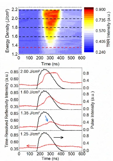
The melt threshold was first detected by in-situ Time-Resolved Reflectometry (TRR). As the liquid SiGe phase has a higher reflectivity than the solid SiGe phase, an abrupt increase in the signal intensity was observed when part of the layer melted [30]. A signal proportional to surface reflectivity was recorded as a function of time for each energy density and plotted in a color map, as shown in Figure 1a, for a 30 nm-thick Si0.6Ge0.4 layer. In this plot, each horizontal line
corresponds to the signal recorded during the laser anneal at a given energy density. It shows how its intensity evolves with time. All the signals were then stacked next to each other, showing the evolution with increasing energy density in the vertical axis. Individual signals for four selected laser energy densities are presented in Figure 1b. At 1.25 J/cm², the slight signal bump between 200 and 400 ns is due to the heating of the solid (i.e. unmelted) SiGe layer. For energy densities equal or higher than 1.35 J/cm², a peak due by the emergence of the liquid phase is observed (cf. blue arrow in Figure 1b). For this 30 nm-thick Si0.6Ge0.4 layer, the melt threshold is close to 1.35 J/cm² (cf. red dotted line in Figure 1a).
As the energy density increased, this peak became larger and more intense, indicating an increasing melt duration and a thicker liquid layer. Above 1.85 J/cm², the reflectivity signal intensity saturated because the liquid layer thickness exceeded the maximum depth probed by the laser ( = 635 nm, incidence angle = 45°) used for TRR measurements. This plateau appears for silicon when the liquid layer is roughly 20 nm-thick [31]. Experimental results on SiGe have shown its appearance for melt depths around 21 nm.
Figure 1. Color map (a) of the TRR signals obtained during the laser annealing of a 30 nm thick Si0.6Ge0.4 layer, showing the evolution
as a function of time and energy density. The red dotted line indicates the melt threshold, at 1.35 J/cm². Individual profiles are shown in (b) for energy densities ranging from 1.25 J/cm² to 2.00 J/cm². At 1.25 J/cm², no sign of melt can be observed. The melt signal appears at 1.35 J/cm² and becomes more intense with increasing energy density.
Partial and full SiGe layer melt regimes can be discriminated with Ge depth profiles: for instance, in the full melt regime, the melted layer is thicker than the initial SiGe layer. Ge atoms redistribution therefore occurs deeper than the original SiGe/Si interface. SIMS depth profiles are presented in Figure 2 for 30 nm thick Si0.6Ge0.4 samples submitted to five laser
energy densities corresponding to the dotted lines added on the TRR map in Figure 1a. Close to the melt threshold, at 1.35 J/cm², the Ge profile remained identical to that of the non-annealed sample and showed no sign of Ge redistribution, with a Si/SiGe interface located at ~31 nm below the surface. Signs of melt and Ge segregation are clearly visible at 1.60 J/cm², with a small Ge depletion detected at a depth close to 10 nm and a higher Ge content near the surface. The Ge content remained unchanged at 39% for the lower and unmelted part of the layer. The sample annealed at 1.81 J/cm² showed similar results, with a higher melt depth and a more pronounced depletion. In both samples, the position of the Si/SiGe interface remained unchanged during the anneal, indicating that a partial melt of the SiGe layer occurred in this case. For 2.00 J/cm², the melt depth was close to the Si/SiGe interface, while the segregation mechanism caused a progressive increase of the Ge content through the layer, similarly to the previous cases. Finally, at 2.20 J/cm², the Ge profile showed that Ge diffused beyond the initial SiGe epi-layer/Si interface, indicating that the full melt regime was reached: the full SiGe layer and part of the Si substrate underneath were melted. For this 30 nm-thick Si0.6Ge0.4 layer, the
Figure 2. ToF-SIMS atomic germanium depth profiles for 30 nm thick Si0.6Ge0.4 samples annealed at laser energy densities from
1.35 J/cm² to 2.20 J/cm².
STEM-HAADF micrographs for the 30 nm-thick Si0.6Ge0.4 samples annealed at 1.81, 2.00 and 2.20 J/cm² are shown in
Figure 3. In the STEM-HAADF mode, the image becomes brighter when the atomic number of the elements in the TEM lamella increases (z-contrast). The Ge-rich areas were therefore brighter in these images, enabling to identify the Si and SiGe layers together with the areas where segregation occurred. At 1.81 J/cm² (Figure 3a), the unmelted part at the bottom of the SiGe layer appeared bright and with a uniform contrast, while the darker area above showed the depletion caused by segregation. The position of the liquid/solid (l/s) interface at maximum melt depth was therefore easily detectable (black arrow in Figure 3). That interface was then rough. Finally, the surface exhibited a brighter contrast due to the higher content of Ge displaced there upon solidification. At 2.00 J/cm² (Figure 3b), the full melt was almost reached and the unmelted layer barely visible. At this energy density, the l/s interface appeared much smoother. Finally, Figure 3c confirmed that, at 2.20 J/cm², the full melt was reached, with a melt depth of 45 nm, i.e. 15 nm within the initial Si substrate (cf. dashed black line). In this case, the l/s interface was also smooth.
Figure 3. STEM-HAADF micrographs of 30 nm Si0.6Ge0.4 samplesannealed at 1.81 J/cm² (a), 2.00 J/cm² (b) and 2.20 J/cm² (c). The
and melted areas where segregation occurred. The dotted lines on the side indicate the original depth of the Si/SiGe interface, while the arrows show the melt depth.
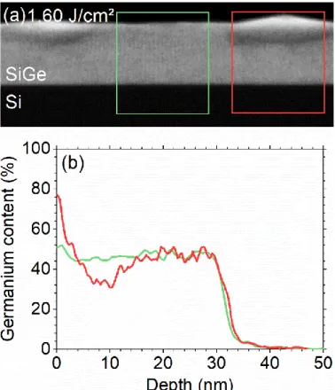
III.1.b. Surface structures at the melt threshold
Similar STEM-HAADF observations were performed on 30 nm-thick Si0.6Ge0.4 samples annealed with energy densities
close to the melt threshold, at 1.40 and 1.60 J/cm². Figure 4a shows one of the micrographs collected at 1.60 J/cm². Surface hillocks can be noticed. The centre of the observed area was flat, with a uniform contrast, while both sides showed hillocks with chemical contrast variations. Identical hillocks could be seen on the whole TEM cross-section and on the sample annealed with a lower energy density (1.40 J/cm²). Germanium STEM-EDX profiles were performed on the areas corresponding to the red and green squares. They are plotted as a function of depth in Figure 4b. The green profile, with an almost constant Ge content (~40%), corresponds to the flat area in the centre. It thus corresponds to an unmelted area since no segregation occurred. In contrast, the red profile obtained on the hillock showed that the layer had melted down to almost 10 nm in this area during anneal, with significant Ge surface segregation.
Figure 4. STEM-HAADF (a) micrograph on a 30 nm thick Si0.6Ge0.4 sample with hillocks on the surface after laser annealing at
1.60 J/cm². EDX germanium depth profiles corresponding to the green and red areas are shown in (b). The flat area showed a uniform concentration, while the hillocks were due to Ge segregation.
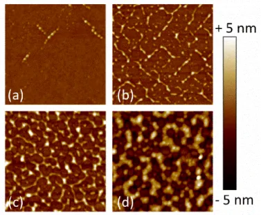
For energy densities slightly above the melt threshold, melted isolated islands are formed instead of a continuous liquid layer. This annealing regime will be referred to as the “surface melt” regime. AFM images gave more insight on these structures and their evolution. 1×1 µm² scans are shown in Figure 5 for energy densities between 1.32 J/cm² and
1.60 J/cm². At 1.32 J/cm², AFM scans show some hillocks (groups of aligned white dots) a few nm above the initially flat epilayer. With increasing laser energy density, these nanostructures become wider, denser, and start to merge. At
1.60 J/cm², about 50% of the surface is covered by hillocks. The average size of hillocks is in good agreement with what was observed by cross-sectional TEM for the same sample. The few hillocks were 70 nm wide and 6 nm high in TEM. Meanwhile, the roughly 60 structures investigated by AFM had a mean width of ~80 nm and a mean height of ~4 nm. Hence, it can be safely concluded that the nanostructures detected by AFM are those observed by TEM and that they are due to the same phenomenon: the progressive melting and covering of the surface by isolated melted islands.
Complementary SP2 Haze analysis (not shown) was performed to track the evolution of the surface quality with the energy density, as already done for Si0.8Ge0.2 in a previous work [28]. It was shown that the surface quality was degraded
1.78 J/cm², suggesting the end of the surface melt regime and the formation of a continuous liquid layer covering the entire surface (referred to as the “partial melt” regime).
Similar surface structures have already been observed at the early stages of melting induced by NLA of Si and Ge [32,33] or millisecond Flash Lamp Annealing of Si, Ge and SiC [34–36]. Similarly to our case, these structures have also been interpreted as the consequence of a local melt of the material at the beginning of the melting process. However, it is important to note that, in previous works, the occurrence of local surface melt was indirectly inferred from time-resolved ellipsometry [33] or transient diffraction measurements [32] recorded during the anneal. In contrast, thanks to the Ge segregation mechanism occurring during the re-solidification of SiGe layers, our results (cf. Figure 4) provide a direct evidence that the melting process starts with the formation of isolated liquid islands.
As for the origin of the observed local melting, this is most probably due to the nucleation occurring during the first-order solid-liquid phase transition [34], although laser radiation variability has also been proposed as a possible explanation [33]. In addition, it is known that the free surface may provide sites for heterogeneous nucleation to occur, allowing surface melt nucleation at temperatures lower than the melting temperature of the bulk solid [37]. However, the detailed determination of the surface melting process (still under debate [38]) is beyond the scope of this paper.
Figure 5. 1×1 µm² AFM scans on 30 nm thick Si0.6Ge0.4 samples annealed at (a) 1.32 J/cm², (b) 1.40 J/cm², (c) 1.50 J/cm² and (d)
1.60 J/cm². The sides of the scans are parallel to the <110> directions. Hillocks appear on the surface at the melt threshold. At higher energy densities, they become denser and merge, until they fully cover the surface.
In summary, four laser annealing regimes were identified for the 30 nm-thick Si0.6Ge0.4 test structure, starting with the
“sub-melt” in which the layer was heated but remained unchanged. Just above the melt threshold, from 1.35 J/cm² to 1.78 J/cm², a “surface melt” regime was identified, with the formation of isolated melted islands. The regimes which followed were the “partial melt” where the whole surface melted, resulting in the formation of a continuous liquid layer progressing towards the SiGe/Si interface when increasing the laser energy density, and finally, the “full melt”, where the SiGe layer and part of the substrate were melted. The full melt threshold was found to be between 2.00 and 2.20 J/cm².
III.1.c. Germanium impact on regime determination
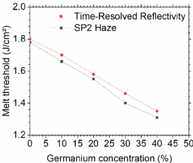
These regimes were investigated for all Ge concentrations considered in this paper, starting from the melt threshold. Both in-situ TRR or SP2 Haze can be used for that purpose, since the surface roughness significantly increases in the surface melt regime. The melt thresholds measured with both methods are plotted in Figure 6 as a function of the Ge
concentration. They clearly follow the same trend. The energy density necessary to reach the melt decreased as the germanium content in the epi-layer increased. This is consistent with the lower melt temperature of a Ge-rich alloy (Tmelt
(Si) = 1414°C Tmelt (Ge) = 938°C). It is worth noting that SP2 Haze always detected the onset of melt at a slightly
lower energy density compared to TRR. This is likely due to the higher sensitivity of the SP2 Haze technique to the presence of surface nanostructures able to scatter light and resulting from isolated molten regions, whereas a larger melted volume is most likely necessary in order to generate a detectable TRR signal.
Figure 6. Evolution of the laser energy density melt threshold as a function of the Ge content in 30 nm-thick SiGe layers. The red and black curves correspond to the results coming from TRR and SP2 haze, respectively.
AFM scans have otherwise shown that the surface melt regime occurs for all Ge concentrations, including bulk silicon. This proved that the local melt was not specifically related to the presence of germanium, or to the alloy properties. 1×1 µm² AFM scans corresponding to the very beginning of the surface melt regime can be seen in Figure 7, for all Ge concentrations. The sides of the scans are parallel to the <110> crystallographic directions. Shape differences are
noticeable: as the Ge content increased, the structures were found to be smaller and exhibited a star-like shape rather than a square one. The observed shapes suggest that the melt and growth of the hillocks occurred preferably along the <100> directions rather than the <110> directions. This trend became more pronounced for higher Ge contents. In addition, the height and width of the hillocks decreased as the Ge content increased.
Figure 7. 1×1 µm² AFM scans after the laser annealing of (a) bulk Si at 1.78 J/cm², (b) Si0.9Ge0.1 at 1.66 J/cm² , (c) Si0.8Ge0.2 at 1.55
J/cm² , (d) Si0.7Ge0.3 at 1.45 J/cm² and (e) Si0.6Ge0.4 at 1.32 J/cm² . They correspond to the first energy density where structures could
be observed on the surface by AFM. Scan sides are parallel to <110> directions.
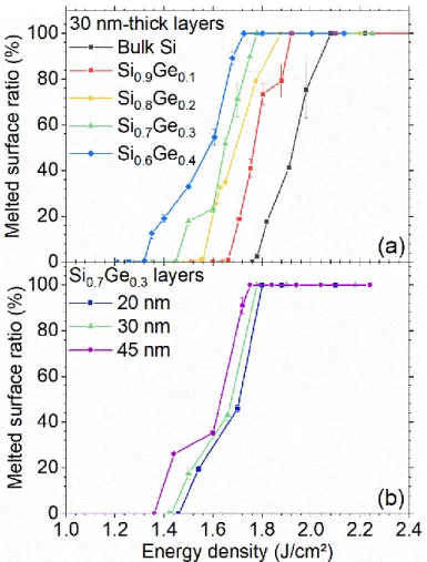
The surface covered by the hillocks (i.e. the melted surface) was inferred from 10×10 µm² AFM images. It is plotted for each concentration in Figure 8a as a function of the laser energy density. There is always a rather linear increase of the covered surface as a function of energy, with a starting point shifted towards lower energy densities when increasing the Ge content. This is due to a decrease of the melting temperature for higher Ge concentrations. In addition, the energy interval between 0% and 100% surface coverage increases with the Ge content: it is equal to 0.33, 0.36, 0.40 and 0.47 J/cm² for 10%, 20%, 30% and 40% of Ge. This suggests that the nucleation rate of the surface islands or their growth rate (or both) decreases with higher Ge contents. More investigations will be necessary to clarify this point. The same measurements were performed on the “Si0.7Ge0.3” sample series, i.e. with constant Ge content (Si0.7Ge0.3) and
different layer thicknesses. The laser energy density melt threshold was slightly reduced when increasing the layer thickness. This was likely due to the lower thermal conductivity of SiGe compared to Si. The evolution of the three samples was otherwise very similar, as shown in Figure 8b. It thus seems that the layer thickness has a small impact on the onset of the surface melt regime.
Figure 8. Evolution of the melted surface coverage as a function of energy density for all Ge concentrations for 30 nm-thick layers (a), and for varying thickness at 30% at.Ge (b). Data were coming from 10×10 µm² AFM images. Additional points were taken from SP2 haze measurements: the last point before SP2 Haze increase is considered to have 0% of melted surface, while the first point after the end of the peak is at 100%.
Chemical profiles were obtained by STEM-EDX or SIMS for both samples series (i.e. “30 nm” and “Si0.7Ge0.3”). The Ge
depth profiles are not shown here, as their shapes are very similar to the ones shown in Figure 2 (those associated with the 30nm thick Si0.8Ge0.2 and Si0.6Ge0.4 samples were reported in previous papers [28,39]. For energy densities
corresponding to the early stages of the surface melt regime (i.e. with a very low percentage of melted surface), SIMS measurements were not able to detect any traces of Ge segregation, the overall signal being dominated by the much larger unmelted surface. In all other cases, Ge segregation was detected and confirmed the accumulation of high Ge concentrations at the surface. Finally, the transition from partial melt to full melt was detected between 2.00 and 2.20 J/cm² in all samples.
Figure 9. Summary of the regimes observed with increasing energy density, for all thicknesses and Ge concentrations investigated here. The blank range between partial melt and full melt corresponds to the energy range where no chemical profiles were obtained. Thus, the exact limit between those regimes is unknown.
The regimes evidenced and the corresponding energy densities for the transition from one regime to the next are
summarised in Figure 9. Each column in it corresponds to a given sample (i.e. a thickness-concentration pair), while each colour corresponds to a given annealing regime. On the left are presented results for the “30 nm” sample series (including the reference “0 %” bulk Si), while results from the “Si0.7Ge0.3” series are presented on the right. It should be noted that
two nominally identical samples are present in both series (i.e. 30 nm-thick Si0.7Ge0.3), with slightly different results. This
is due to the small difference in pulse duration used when annealing the two sample series (145 ns for the “30 nm” series, 160 ns for the “Si0.7Ge0.3” series).
III.2. Strain relaxation
In addition to the evolution of the surface roughness and Ge depth distribution as a function of the laser anneal conditions, we also explored the evolution of the compressive strain in the same Si1-xGex layers for each annealing
regime. Similarly to the approach followed in the previous section, we will first focus on the behavior of the Si0.6Ge0.4
samples upon laser annealing at various energy densities. We will then extend the discussion to the other samples to take into account the impact of the initial Ge content and of the layer thickness on the SiGe strain relaxation mechanism.
III.2.a. Relaxation of the 30 nm-thick Si0.6Ge0.4 structure
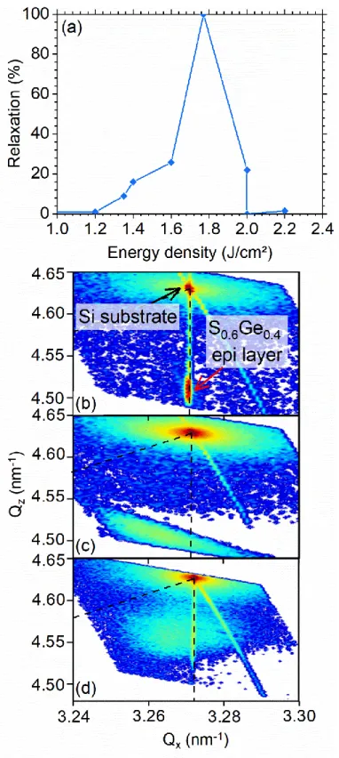
Reciprocal Space Maps (RSM) around the (224) diffraction order were used to obtain macroscopic degrees of strain relaxation R for all annealing regimes in Si0.6Ge0.4 samples.
𝑅 =
𝑎𝑆𝑖𝐺𝑒 //−𝑎𝑆𝑖
𝑎𝑆𝑖𝐺𝑒0 −𝑎𝑆𝑖 [1]
Where 𝑎𝑆𝑖𝐺𝑒// is the in plane lattice parameter of strained SiGe, 𝑎𝑆𝑖𝐺𝑒0 is the lattice parameter of relaxed SiGe and 𝑎𝑆𝑖 the
lattice parameter of relaxed Si (𝑎𝑆𝑖=5.43105Ǻ). Results are summarised in Figure 10 where the degree of relaxation is
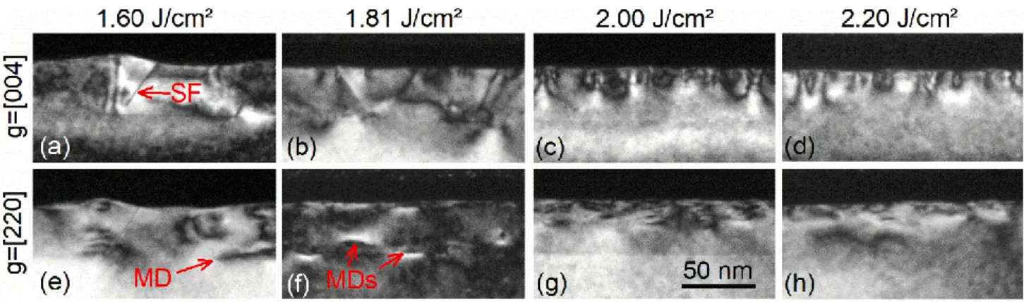
plotted as a function of the laser energy density (Figure 10a) while RSMs from selected samples are presented in Figures 10b, c and d. Dark Field (DF) TEM micrographs from samples annealed at energies from 1.60 J/cm2 to
2.20 J/cm2 are presented in Figure 11. Two diffracting vectors were used for each sample: g=[004] (Figures 11a to 11d)
and g=[220] (Figures 11e to 11h).
As-grown samples were as expected pseudomorphic. They remained so after annealing in the sub-melt regime (cf. Figure 10b).
Partial relaxation occurred for samples in the surface melt regime, with a degree of relaxation that increased with the laser energy density, i.e. from 10% at 1.35 J/cm2 up to 26% at 1.60 J/cm2 (cf. Figure 10c). DF-TEM micrographs from
the sample annealed at 1.60 J/cm² (cf. Figures 11a and 11e) showed defects over the whole thickness, even at depths that did not melt during the laser anneal. The defects observed consisted mostly of (111) Stacking Faults (SFs) located beneath the melted islands. Some misfit dislocations (MDs) parallel to the SiGe interface were also occasionally observed.
The partial melt regime gave dissimilar results: for a laser energy density of 1.81 J/cm², the layer was found to be totally relaxed. The corresponding TEM images (Figures 11b and f) confirm this result, by showing an increased density of defects, including both SFs and MDs, the latter being more effective in relieving elastic strain [40]. In contrast, at 2.00 J/cm2 (i.e. at the threshold between the partial and the full melt regime), the annealing process resulted in a bilayer
made of a fully strained part and a partially relaxed part (with R = 22%, cf. Figures 10a and d). Indeed, the corresponding TEM images (cf. Figures 11c and g) show that, in this case, the defect band (related to relaxation) is confined within a surface layer ~15 nm thick, while the underlying layer, down to the SiGe/Si interface, is defect free and therefore the fully strained region detected by XRD.
Figure 10. Evolution of the macroscopic degree of relaxation as a function of the laser energy density for 30 nm-thick Si0.6Ge0.4 layers
(a). These datas were obtained from (224) XRD RSM such as the ones shown in (b, c, d). The RSM presented here correspond to Si0.6Ge0.4 layers after annealing at 1.20 J/cm² (d), 1.60 J/cm²(c) and 2.00 J/cm²(d). At 1.20 J/cm², the RSM is identical to the reference
RSM and correspond to a strained sample. At 1.60 J/cm², the SiGe peak shifts towards lower QX (and therefore higher in-plane lattice
parameter than that of bulk Si), indicating partial relaxation. At 2.00 J/cm², two peaks can be observed: a partially relaxed contrbution and a strained contribution.
Finally, a similar result was obtained for the sample annealed in the full melt regime (2.20 J/cm2). A bilayer was also
observed by XRD in that case (not shown here), even though the degree of relaxation of the partially relaxed layer could not be measured due to the low intensity of the XRD signal. Again, the dark-field TEM micrographs from this sample
confirm this result (cf. Figures 11d and h), by showing that the lower part of the SiGe layer exhibited no defects, while the defective region was confined within the first 15 nm below the surface.
These results can be qualitatively explained by considering the impact the liquid/solid interface roughness has on the solidification mechanism, similarly to what is observed during the Low Temperature Solid Phase Epitaxial Regrowth (LT-SPER) of amorphised SiGe/Si epi-layers. For amorphous layers obtained by Ion Implantation and extending beyond the SiGe layer into the Si substrate [41,42], it was found that, during recrystallization, the initially flat
amorphous/crystalline (a/c) interface progressively transformed into a faceted one (along {111} planes) when it moved through the SiGe layer, with a roughness that increased proportionally to the Ge content. In turn, the interface roughness favours the formation of strain relieving defects (including SFs and MDs), provided the elastic energy stored in the layer exceeds a critical value [43]. For SiGe layers obtained by ion beam synthesis (i.e. high dose Ge+ ion implantation), the
critical elastic energy value for strain relaxation was estimated at ~300 mJ/m2 [44]. In contrast to such “elastic
energy-driven” relaxation mechanism, when the regrowth started inside the SiGe layer, extended defects were formed in the whole regrown layer, regardless of the Ge content, eventually leading to some strain relaxation [45].
SiGe NLA investigated here shares some similarities with the regrowth mechanism controlling the LT-SPER of amorphised SiGe. Indeed, we could identify several samples in which solidification started inside the SiGe layer and resulted in the formation of strain relieving extended defects throughout the whole SiGe layer, independently of the Ge content, including the Si0.6Ge0.4 samples annealed at 1.60 J/cm² (cf. Figures 11a and e) or at 1.81 J/cm2 (cf. Figures 11b
and f). Thanks to STEM-HAADF, the morphology of the liquid/solid (l/s) interface at maximum melt, i.e. at the beginning of solidification, was determined for both samples. In both cases, solidification started from a non-planar l/s interface. In particular, in the sample annealed at 1.60 J/cm² (cf. Figure 4a, surface melt regime), the isolated liquid islands present on the surface exhibited a curved liquid/solid interface. They were thus likely to induce regrowth along different crystallographic directions, favouring the formation of strain relieving defects. STEM-HAADF observations clearly showed a rough l/s interface for the sample annealed at 1.81 J/cm2 (cf. Figure 3a, partial melt regime), with a
variation of several nanometres in the interface depth. Finally, in both cases, the defects formed during annealing caused some strain relaxation. In particular, partial relaxation (~26%) was found in the sample annealed at 1.60 J/cm², when only half of the surface melted during the anneal. Meanwhile, a 100% relaxation was measured when a continuous liquid layer was obtained at 1.81 J/cm².
Figure 11. Cross sectional TEM images in the Dark Field mode of 30 nm thick Si0.6Ge0.4 layers annealed at laser energy densities
ranging from 1.60 to 2.20 J/cm². For each sample, 2 diffracting vectors were used: g = [004] and [220]. Some stacking faults (SF) and misfit dislocations (MD) are highlighted by red arrows. These micrographs highlighted the strain around crystalline defects in the layers. Strain relieving defects were formed beneath the surface nanostructures (hillocks) at 1.60 J/cm², down to the bottom of the layer. At 2.20 J/cm², the initial SiGe was changed into a bilayer with a relaxed area confined in the upper part (~12 nm).
On the other hand, samples annealed at 2.00 J/cm2 (end of the partial melt regime) or 2.20 J/cm² (full melt regime)
seemed to follow the “elastic energy-driven” relaxation mechanism discussed above for LT-SPER. Indeed, in both cases, solidification started from a flat interface, as shown in Figure 3b and c, respectively, resulting in defect-free bottom layers capped with layers containing stress relieving defects, as found by DF-TEM analysis (cf. Figures 11c-d and g-h) and in agreement with the “bilayer” observed by XRD in the same samples (cf. Figure 10d). It can be therefore inferred that interface roughening and the formation of a large amount of defects occur when the elastic energy stored in the regrown layer exceeds a critical value.
In order to estimate the amount of elastic energy stored in the samples investigated in this work, we modified the simple calculation given for SiGe layers with constant Ge content [46] to that the Ge redistribution during laser annealing could be taken into account. For this, the graded Ge profile was dividing the layer into multiple sub-layers, as shown in Figure 13. The elastic energy stored (J/m²) can then be expressed as :
𝐸 = ∫
𝑧=𝑠𝑢𝑟𝑓𝑎𝑐𝑒𝑧=𝑙𝑎𝑦𝑒𝑟 𝑡ℎ𝑖𝑐𝑘𝑛𝑒𝑠𝑠𝐵 ∙ 𝜀(𝑧)
²∙ 𝑑𝑧
[2]
Where
𝐵 = 2µ(𝑧) ∙
1 + 𝜈(𝑧)1 − 𝜈(𝑧)
[3]
And
𝜀(𝑧) =
𝑎𝑆𝑖𝐺𝑒−𝑎𝑆𝑖𝑎𝑆𝑖
[4]
Where zmax is the thickness of the SiGe layer, ε(z) is the strain, µ(z) the shear modulus and ν(z) the Poisson’s ratio. For the
calculations presented here, the sub-layer’s thickness was chosen constant at 0.5 nm. The Ge content for each sub-layer was determined by modelling the experimental profiles obtained from SIMS or EDX. The strain, shear modulus and Poisson’s ratio are all dependant on the Ge content in the sublayer, and thus on depth. They were derived from the elastic constants C11 and C12 [47].
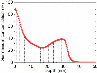
Figure 12. Ge profile for a 30 nm-thick Si0.6Ge0.4 sample annealed at 1.81 J/cm² with a schematic representation of the slicing used to
model the Ge depth profile and calculate the elastic energy stored in the SiGe layers after laser annealing. In practice, sub-layers were 0.5 nm-thick.
For the Si0.6Ge0.4 samples annealed at 2.00 J/cm2 or 2.20 J/cm², the elastic energies stored in the regrown layers were of
~1950 mJ/m2 and ~1190 mJ/m2, respectively. These values are much higher than those previously determined for Ion
Beam Synthesised SiGe layers (~300 mJ/m2). It is therefore not surprising that strain relaxation was observed in these
samples. In the following section, relaxation measurements will be presented for the different samples and results discussed in terms of elastic energy stored.
III.2.b. Impact of Ge concentration and/or thickness
Strain relaxation measurements were performed in the same manner for all layers. The results for the “30 nm” series (different initial Ge concentrations) are shown in Figure 13a while those related to the “Si0.7Ge0.3” series (different layer
thicknesses) are plotted in Figure 13b.
As-grown samples were as expected found to be perfectly strained, as well as all samples annealed in the sub-melt regime, i.e. independently of the initial Ge content. In addition, the Si0.9Ge0.1 samples (red squares in Figure 13a) did not
show any relaxation regardless of the annealing regime it underwent (surface, partial or full melt regimes), in agreement with the low level of elastic energy stored in such layers (never exceeding 130 mJ/m2).
For Si0.8Ge0.2 samples, (yellow circles in Figure 13a), it was found that, in the surface melt regime (at 1.55 and
1.59 J/cm²), laser annealing did not cause any relaxation, although the surface had locally started to melt (with a surface coverage lower than 20%, however). For higher energy densities, at the end of the surface melt regime (1.70 and
1.80 J/cm²), solidification started from a non-planar l/s interface [28], leading to the same results as those described in the previous section, i.e. the formation of defects in the whole regrown layer, accompanied by partial relaxation (~30% in this case). Finally, for even higher laser energies (2.00 and 2.20 J/cm2), the l/s interface at maximum melt was found to
be perfectly flat [28]. An “elastic energy-driven” relaxation mechanism is thus to be expected. Indeed, no defects were observed by TEM in those samples, which were fully strained (cf. Figure 13a), suggesting that the elastic energy stored
in these samples (~330 mJ/m2 and ~280 mJ/m2 after annealing at 2.00 and 2.20 J/cm2, respectively) was lower than the
critical value for relaxation.
Results for the Si0.7Ge0.3 samples (green triangles in Figure 13a) were once again consistent with the scenario described
above. In particular, a fully strained structure was obtained after annealing at 2.20 J/cm2, corresponding to an elastic
energy of ~640 mJ/m2.
Finally, for Si0.7Ge0.3 samples 20, 30 or 45 nm thick (Figure 13b), the surface melt regime once again led to layers with a
degree of relaxation close to 30%. The onset of relaxation occurred at lower laser energy density for the thickest sample, in agreement with its earlier melt threshold. Similarly, higher relaxation levels (up to 100%) were found for the 45 nm-thick sample compared to the thinner ones. Finally, fully strained regrowth was only achieved for the thinner layers at energy densities higher than 2.00 J/cm2. Meanwhile, anneals at 2.04 and 2.24 J/cm² of the 45 nm-thick sample resulted in
bilayers made of a fully strained part and a partially relaxed part (~17% at 2.04 J/cm², cf. Figure 13b). The relaxation value for the upper layer could not be measured for the sample annealed at 2.24 J/cm², due to its low intensity, similarly to what occurred for Si0.6Ge0.4 annealed at 2.20 J/cm².
Figure 13. Evolution of the macroscopic degree of strain relaxation as a function of laser energy density for (a) 30 nm-thick layers with Ge contents ranging from 0% to 40%, and (b) for Si0.7Ge0.3 layers at 20, 30 or 45 nm. Some plots exhibits two relaxation values
for a given energy density: it is caused by the appearance of two SiGe peaks in the RSM. An example of such a map can be found in Figure 10b.
Results obtained here are consistent with examples from the literature where strained layers were also obtained when the final Ge content was low and the l/s interface at maximum melt was deeper than the original SiGe/Si interface [23– 25,27]. The bilayers obtained by Kociniewski et al.[24] were likely related to the high Ge content in the final layers. They disappeared when the Ge was diluted at higher energy densities, which reduced the stored elastic energy.
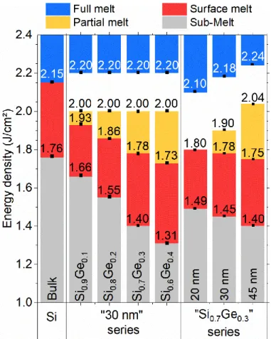
Our results clearly indicate that, when solidification starts from a flat l/s interface, the relaxation mechanism is driven by the amount of elastic energy stored in the regrown structures. For all samples with such a relaxation mechanism, we have therefore plotted the corresponding values of the elastic energy in Figure 14. In it, solid symbols correspond to fully strained samples, whereas empty symbols indicate samples with a “bilayer” structure, i.e. a defect-free region in the
lower part of the regrown layer and a defective layer at the surface, which forms when the critical elastic energy value was exceeded. The threshold for strain relaxation is around 750 mJ/m². Fully pseudomorphic regrowth will occur for SiGe/Si epilayers subjected to melt NLA only if the built-in elastic energy is lower than this threshold. While being well above the value previously determined for Ion Beam Synthesised SiGe layers (~300 mJ/m2), the critical elastic energy
for NLA SiGe layers is lower than the one achieved for CVD grown SiGe layer with constant Ge concentrations [29,43]. However, NLA offers more versatility by enabling the formation of steep Ge gradients with concentration levels at the surface as high as 80% at., which are beneficial for several applications, including source/drain contact engineering.
Figure 14. Total elastic energy density in SiGe layers after laser anneal. Results are shown only for layers with a smooth l/s interface. The ones at constant thickness are on the left, and the ones at varying thicknesses on the right of the graph. Layers that were perfectly strained are represented by full squares, while the ones with a bilayer are represented by open symbols. A separation can be observed near 750 mJ/m².
IV. Conclusion
The impact of Ultraviolet Nanosecond Laser Anneal on pseudomorphic Si1-xGex layers with various Ge contents (from
x=0 to 0.4) and thicknesses (20, 30 and 45 nm) was investigated, in order to understand the impact of these parameters on the annealing regimes and on the relaxation of the initial compressive strain. Similar regimes were observed for each concentration and each thickness: the sub-melt, the surface melt, the partial melt and the full melt. There were no differences between as-grown and sub-melt samples. Locally melted islands that grew and merged with increasing laser energy densities were obtained on surface melt samples. The partial melt was reached when a continuous liquid layer covered the surface during the laser pulse and the melt front remained in the original SiGe layer. In this regime, the melt front was rough. Finally, the full melt was reached when the melt front reached at least the initial Si/SiGe interface, with a smooth l/s interface in that case. The Ge content influenced the regimes Layers reached the melt threshold at lower energy densities when the Ge content was higher. However, the full melt was often reached for energy densities between 2.00 and 2.20 J/cm². Germanium segregation was observed in all melt regimes, resulting in the formation of gradients and the presence of high Ge contents close to the surface. The surface Ge concentration was at its highest for energy densities corresponding to the end of partial melt/beginning of full melt.
The strain relaxation is linked to the l/s interface roughness and to the amount of elastic energy stored in the layer. A rough melt front (in surface and partial melt regimes) facilitates defect formation, resulting in partial relaxation (~30%) for layers with low elastic energies (i.e. low Ge content and/or low thickness) and full relaxation in layers with high elastic energies. In each case, the rough interface most likely leads to defect formation, with defects crossing the whole layer evidenced by TEM. On the other hand, in layers where the laser annealing conditions led to a smooth liquid/solid
interface, the relaxation is only linked to the amount of elastic energy stored in the layer. Pseudomorphic regrowth is possible for layers with low built-in elastic energies. Above a critical level, around 750 mJ/m², laser annealed Si1-xGex
form bilayers, where the lower part is pseudomorphic and the upper part is partially relaxed. While this critical level is lower than the one for standard epitaxy, NLA offers the possibility to form steep gradients with high Ge contents near the surface and therefore more performant contacts.
Declaration of Interests
The authors declare that they have no known competing financial interests or personal relationships that could have appeared to influence the work reported in this paper.
Acknowledgments
SCREEN company and its French subsidiary LASSE are gratefully acknowledged for their support in operating and maintaining the LT-3100 laser annealing platform. We also thank the Raimond Castaing platform in Toulouse for its support in micro characterization.
References
[1] T. Manku, J.M. McGregor, A. Nathan, D.J. Roulston, J.- Noel, D.C. Houghton, Drift hole mobility in strained and unstrained doped Si/sub 1-x/Ge/sub x/ alloys, IEEE Trans. Electron Devices. 40 (1993) 1990–1996.
https://doi.org/10.1109/16.239739.
[2] T. Ghani, M. Armstrong, C. Auth, M. Bost, P. Charvat, G. Glass, T. Hoffmann, K. Johnson, C. Kenyon, J. Klaus, B. McIntyre, K. Mistry, A. Murthy, J. Sandford, M. Silberstein, S. Sivakumar, P. Smith, K. Zawadzki, S. Thompson, M. Bohr, A 90nm high volume manufacturing logic technology featuring novel 45nm gate length strained silicon CMOS transistors, in: IEEE Int. Electron Devices Meet. 2003, 2003: p. 11.6.1-11.6.3.
https://doi.org/10.1109/IEDM.2003.1269442.
[3] W. Skorupa, H. Schmidt, eds., Subsecond Annealing of Advanced Materials: Annealing by Lasers, Flash Lamps and Swift Heavy Ions, Springer International Publishing, 2014. //www.springer.com/la/book/9783319031309 (accessed March 7, 2018).
[4] V. Gonda, Excimer Laser Annealing for Ultrashallow Junctions and Contacts, Technische Universiteit Budapest, Hungary, 2008.
[5] E. Rosseel, S.K. Dhayalan, A.Y. Hikavyy, R. Loo, H.B. Profijt, D. Kohen, S. Kubicek, T. Chiarella, H. Yu, N. Horiguchi, D. Mocuta, K. Barla, A. Thean, G. Bartlett, J. Margetis, N. Bhargava, J. Tolle, Selective Epitaxial Growth of High-P Si:P for Source/Drain Formation in Advanced Si nFETs, ECS Trans. 75 (2016) 347–359.
https://doi.org/10.1149/07508.0347ecst.
[6] S. Heo, H. Hwang, H.T. Cho, W.A. Krull, Ultrashallow (<10nm) p+∕n junction formed by B18H22 cluster ion implantation and excimer laser annealing, Appl. Phys. Lett. 89 (2006) 243516. https://doi.org/10.1063/1.2405863. [7] K. Huet, F. Mazzamuto, T. Tabata, I. Toqué-Tresonne, Y. Mori, Doping of semiconductor devices by Laser Thermal Annealing, Mater. Sci. Semicond. Process. 62 (2017) 92–102. https://doi.org/10.1016/j.mssp.2016.11.008. [8] E. Bruno, G.G. Scapellato, G. Bisognin, E. Carria, L. Romano, A. Carnera, F. Priolo, High-level incorporation of antimony in germanium by laser annealing, J. Appl. Phys. 108 (2010) 124902. https://doi.org/10.1063/1.3520671. [9] F. Cristiano, M. Shayesteh, R. Duffy, K. Huet, F. Mazzamuto, Y. Qiu, M. Quillec, H.H. Henrichsen, P.F. Nielsen, D.H. Petersen, A. La Magna, G. Caruso, S. Boninelli, Defect evolution and dopant activation in laser annealed Si and Ge, Mater. Sci. Semicond. Process. 42 (2016) 188–195. https://doi.org/10.1016/j.mssp.2015.09.011.
[10] C. Fenouillet-Beranger, P. Batude, L. Brunet, V. Mazzocchi, C.M.V. Lu, F. Deprat, J. Micout, M.P. Samson, B. Previtali, P. Besombes, N. Rambal, V. Lapras, F. Andrieu, O. Billoint, M. Brocard, S. Thuries, G. Cibrario, P. Acosta-Alba, B. Mathieu, S. Kerdilès, F. Nemouchi, C. Arvet, P. Besson, V. Loup, R. Gassilloud, X. Garros, C. Leroux, V. Beugin, C. Guerin, D. Benoit, L. Pasini, J.M. Hartmann, M. Vinet, Recent advances in low temperature process in view of 3D VLSI integration, in: 2016 IEEE SOI-3D-Subthreshold Microelectron. Technol. Unified Conf. S3S, 2016: pp. 1–3. https://doi.org/10.1109/S3S.2016.7804404.
[11] P. Batude, C. Fenouillet-Beranger, L. Pasini, V. Lu, F. Deprat, L. Brunet, B. Sklenard, F. Piegas-Luce, M. Cassé, B. Mathieu, O. Billoint, G. Cibrario, O. Turkyilmaz, H. Sarhan, S. Thuries, L. Hutin, S. Sollier, J. Widiez, L. Hortemel, C. Tabone, M.P. Samson, B. Previtali, N. Rambal, F. Ponthenier, J. Mazurier, R. Beneyton, M. Bidaud, E. Josse, E. Petitprez, O. Rozeau, M. Rivoire, C. Euvard-Colnat, A. Seignard, F. Fournel, L. Benaissa, P. Coudrain, P. Leduc, J.M. Hartmann, P. Besson, S. Kerdiles, C. Bout, F. Nemouchi, A. Royer, C. Agraffeil, G. Ghibaudo, T. Signamarcheix, M. Haond, F. Clermidy, O. Faynot, M. Vinet, 3DVLSI with CoolCube process: An alternative path to scaling, in: 2015 Symp. VLSI Technol. VLSI Technol., 2015: pp. T48–T49.
https://doi.org/10.1109/VLSIT.2015.7223698.
[12] S. Kerdilès, P. Acosta-Alba, B. Mathieu, M. Veillerot, H. Denis, F. Aussenac, F. Mazzamuto, I. Toque-Tresonne, K. Huet, M.-P. Samson, B. Previtali, L. Brunet, P. Batude, C. Fenouillet-Beranger, Sequential 3D Process Integration: Opportunities for Low Temperature Processing, ECS Trans. 80 (2017) 215–225.
https://doi.org/10.1149/08004.0215ecst.
[13] C. Fenouillet-Beranger, B. Mathieu, B. Previtali, M.P. Samson, N. Rambal, V. Benevent, S. Kerdiles, J.P. Barnes, D. Barge, P. Besson, R. Kachtouli, M. Cassé, X. Garros, A. Laurent, F. Nemouchi, K. Huet, I. Toqué-Trésonne, D. Lafond, H. Dansas, F. Aussenac, G. Druais, P. Perreau, E. Richard, S. Chhun, E. Petitprez, N. Guillot, F. Deprat, L. Pasini, L. Brunet, V. Lu, C. Reita, P. Batude, M. Vinet, New insights on bottom layer thermal stability and laser annealing promises for high performance 3D VLSI, in: 2014 IEEE Int. Electron Devices Meet., 2014: p. 27.5.1-27.5.4. https://doi.org/10.1109/IEDM.2014.7047121.
[14] C.N. Ni, Y.C. Huang, S. Jun, S. Sun, A. Vyas, F. Khaja, K.V. Rao, S. Sharma, N. Breil, M. Jin, C. Lazik, A. Mayur, J. Gelatos, H. Chung, R. Hung, M. Chudzik, N. Yoshida, N. Kim, PMOS contact resistance solution compatible to CMOS integration for 7 nm node and beyond, in: 2016 Int. Symp. VLSI Technol. Syst. Appl. VLSI-TSA, 2016: pp. 1– 2. https://doi.org/10.1109/VLSI-TSA.2016.7480531.
[15] J.L. Everaert, M. Schaekers, H. Yu, L.L. Wang, A. Hikavyy, L. Date, J. del A. Borniquel, K. Hollar, F.A. Khaja, W. Aderhold, A.J. Mayur, J.Y. Lee, H. van Meer, Y.L. Jiang, K.D. Meyer, D. Mocuta, N. Horiguchi, Sub-10E-9
Ohm.cm2 contact resistivity on p-SiGe achieved by Ga doping and nanosecond laser activation, in: 2017 Symp. VLSI Technol., 2017: pp. T214–T215. https://doi.org/10.23919/VLSIT.2017.7998176.
[16] C.Y. Chang, F.A. Khaja, K.E. Hollar, K.V. Rao, C. Lazik, M. Jin, H. Zhou, R. Hung, Y.C. Huang, H. Chung, A. Mayur, N. Kim, Ultra-low (1.2E-9 ohmcm2) p-Si0.55Ge0.45 contact resistivity using nanosecond laser anneal for 7nm nodes and beyond, in: 2017 17th Int. Workshop Junction Technol. IWJT, 2017: pp. 23–26.
https://doi.org/10.23919/IWJT.2017.7966504.
[17] L.L. Wang, H. Yu, M. Schaekers, J.L. Everaert, A. Franquet, B. Douhard, L. Date, J. del A. Borniquel, K. Hollar, F.A. Khaja, W. Aderhold, A.J. Mayur, J.Y. Lee, H. van Meer, D. Mocuta, N. Horiguchi, N. Collaert, K.D. Meyer, Y.L. Jiang, Comprehensive study of Ga activation in Si, SiGe and Ge with 5 #x00D7; 10 #x2212;10 #x03A9;
#x00B7;cm2 contact resistivity achieved on Ga doped Ge using nanosecond laser activation, in: 2017 IEEE Int. Electron Devices Meet. IEDM, 2017: p. 22.4.1-22.4.4. https://doi.org/10.1109/IEDM.2017.8268441.
[18] O. Gluschenkov, H. Wu, K. Brew, C. Niu, L. Yu, Y. Sulehria, S. Choi, C. Durfee, J. Demarest, A. Carr, S. Chen, J. Willis, T. Thanigaivelan, F. Lie, W. Kleemeier, D. Guo, External Resistance Reduction by Nanosecond Laser Anneal in Si/SiGe CMOS Technology, in: 2018 IEEE Int. Electron Devices Meet. IEDM, 2018: p. 35.3.1-35.3.4. https://doi.org/10.1109/IEDM.2018.8614628.
[19] D.P. Brunco, M.O. Thompson, D.E. Hoglund, M.J. Aziz, H. ‐J. Gossmann, Germanium partitioning in silicon during rapid solidification, J. Appl. Phys. 78 (1995) 1575–1582. https://doi.org/10.1063/1.360251.
[20] S.F. Lombardo, S. Boninelli, F. Cristiano, G. Fisicaro, G. Fortunato, M.G. Grimaldi, G. Impellizzeri, M. Italia, A. Marino, R. Milazzo, E. Napolitani, V. Privitera, A. La Magna, Laser annealing in Si and Ge: Anomalous physical aspects and modeling approaches, Mater. Sci. Semicond. Process. 62 (2017) 80–91.
https://doi.org/10.1016/j.mssp.2016.10.047.
[21] C.Y. Ong, K.L. Pey, X. Li, X.C. Wang, C.M. Ng, L. Chan, Laser annealing induced high Ge concentration epitaxial SiGe layer in Si1−xGex virtual substrate, Appl. Phys. Lett. 93 (2008) 041112.
[22] N. Frangis, J. Van Landuyt, R. Larciprete, S. Martelli, E. Borsella, S. Chiussi, J. Castro, B. León, High resolution electron microscopy and x-ray photoelectron spectroscopy studies of heteroepitaxial SixGe(1−x) alloys produced through laser induced processing, Appl. Phys. Lett. 72 (1998) 2877–2879. https://doi.org/10.1063/1.121487. [23] S. Lombardo, K. Kramer, M.O. Thompson, D.R. Smith, Pulsed laser assisted epitaxy of GexSi1−x alloys on Si 〈100〉, Appl. Phys. Lett. 59 (1991) 3455–3457. https://doi.org/10.1063/1.105676.
[24] T. Kociniewski, F. Fossard, J. Boulmer, D. Bouchier, Synthesis of strained SiGe on Si(100) by pulsed laser induced epitaxy, Thin Solid Films. 518 (2010) 2542–2545. https://doi.org/10.1016/j.tsf.2009.09.154.
[25] J.R. Abelson, T.W. Sigmon, K.B. Kim, K.H. Weiner, Epitaxial GeSi/Si (100) structures produced by pulsed laser mixing of evaporated Ge on Si (100) substrates, Appl. Phys. Lett. 52 (1988) 230–232.
https://doi.org/10.1063/1.99528.
[26] G.V. Luong, S. Wirths, S. Stefanov, B. Holländer, J. Schubert, J.C. Conde, T. Stoica, U. Breuer, S. Chiussi, M. Goryll, D. Buca, S. Mantl, Study of dopant activation in biaxially compressively strained SiGe layers using excimer laser annealing, J. Appl. Phys. 113 (2013) 204902. https://doi.org/10.1063/1.4807001.
[27] C.Y. Ong, K.L. Pey, K.K. Ong, D.X.M. Tan, X.C. Wang, H.Y. Zheng, C.M. Ng, L. Chan, A low-cost method of forming epitaxy SiGe on Si substrate by laser annealing, Appl. Phys. Lett. 94 (2009) 082104.
https://doi.org/10.1063/1.3086881.
[28] L. Dagault, P. Acosta-Alba, S. Kerdilès, J.P. Barnes, J.M. Hartmann, P. Gergaud, T.T. Nguyen, A. Grenier, A.M. Papon, N. Bernier, V. Delaye, J. Aubin, F. Cristiano, Impact of UV Nanosecond Laser Annealing on Composition and Strain of Undoped Si0.8Ge0.2 Epitaxial Layers, ECS J. Solid State Sci. Technol. 8 (2019) P202–P208.
https://doi.org/10.1149/2.0191903jss.
[29] J.M. Hartmann, A. Abbadie, S. Favier, Critical thickness for plastic relaxation of SiGe on Si(001) revisited, J. Appl. Phys. 110 (2011) 083529. https://doi.org/10.1063/1.3656989.
[30] J. Boneberg, J. Nedelcu, H. Bender, P. Leiderer, Dynamics of the solidification of laser-annealed Si thin films, Mater. Sci. Eng. A. 173 (1993) 347–350. https://doi.org/10.1016/0921-5093(93)90242-7.
[31] J. Boneberg, P. Leiderer, On the Interpretation of Time-Resolved Surface Reflectivity Measurements during the Laser Annealing of Si Thin Films, Phys. Status Solidi A. 166 (n.d.) 643–650. https://doi.org/10.1002/(SICI)1521-396X(199804)166:2<643::AID-PSSA643>3.0.CO;2-L.
[32] J.F. Young, J.E. Sipe, H.M. van Driel, Laser-induced periodic surface structure. III. Fluence regimes, the role of feedback, and details of the induced topography in germanium, Phys. Rev. B. 30 (1984) 2001–2015.
https://doi.org/10.1103/PhysRevB.30.2001.
[33] G.E. Jellison, D.H. Lowndes, D.N. Mashburn, R.F. Wood, Time-resolved reflectivity measurements on silicon and germanium using a pulsed excimer KrF laser heating beam, Phys. Rev. B. 34 (1986) 2407–2415.
https://doi.org/10.1103/PhysRevB.34.2407.
[34] K.-H. Heinig, Effects of local melting on semiconductor surfaces, Energy Pulse Modif. Semicond. Relat. Mater. (1984) 265–279.
[35] M.P. Smith, R.A. McMahon, M. Voelskow, W. Skorupa, J. Stoemenos, G. Ferro, Process control and melt depth homogenization for SiC-on-Si structures during flash lamp annealing by carbon implantation, J. Appl. Phys. 100 (2006) 094909. https://doi.org/10.1063/1.2359684.
[36] D. Skarlatos, V. Ioannou-Sougleridis, M. Barozzi, G. Pepponi, D. Velessiotis, M.C. Skoulikidou, N.Z. Vouroutzis, K. Papagelis, P. Dimitrakis, C. Thomidis, Phosphorous Diffusion in N2+-Implanted Germanium during Flash Lamp Annealing: Influence of Nitrogen on Ge Substrate Damage and Capping Layer Engineering, ECS J. Solid State Sci. Technol. 6 (2017) P418–P428.
[37] Q.S. Mei, K. Lu, Melting and superheating of crystalline solids: From bulk to nanocrystals, Prog. Mater. Sci. 52 (2007) 1175–1262. https://doi.org/10.1016/j.pmatsci.2007.01.001.
[38] H.T.T. Nguyen, V.V. Hoang, L.N.T. Minh, Melting of crystalline silicon thin films, Comput. Mater. Sci. 89 (2014) 97–101. https://doi.org/10.1016/j.commatsci.2014.03.039.
[39] L. Dagault, S. Kerdilès, P. Acosta-Alba, J.M. Hartmann, J.P. Barnes, P. Gergaud, F. Cristiano, Impact of Germanium Concentration on the Ultraviolet Nanosecond Laser Annealing of Intrinsic Si1-xGex Epitaxial Layers, in: Int. Conf. Solid State Devices Mater., Nagoya, 2019: pp. 567–568.
[40] P.M. Mooney, Strain relaxation and dislocations in SiGe/Si structures, Mater. Sci. Eng. R Rep. 17 (1996) 105– 146. https://doi.org/10.1016/S0927-796X(96)00192-1.
[41] R.G. Elliman, W.C. Wong, The fabrication of epitaxial GexSi1−x layers by ion implantation, Nucl. Instrum. Methods Phys. Res. Sect. B Beam Interact. Mater. At. 80–81 (1993) 768–772.
https://doi.org/10.1016/0168-583X(93)90678-Y.
[42] D.C. Paine, D.J. Howard, N.G. Stoffel, J.A. Horton, The growth of strained Si1−xGex alloys on 〈001〉 silicon using solid phase epitaxy, J. Mater. Res. (1990) 1023–1031.
[43] R. People, J.C. Bean, Calculation of critical layer thickness versus lattice mismatch for GexSi1−x/Si strained‐ layer heterostructures, Appl. Phys. Lett. 47 (1985) 322–324. https://doi.org/10.1063/1.96206.
[44] F. Cristiano, A. Nejim, Y. Suprun-Belevich, A. Claverie, P.L.F. Hemment, Formation of extended defects and strain relaxation in ion beam synthesised SiGe alloys, Nucl. Instrum. Methods Phys. Res. Sect. B Beam Interact. Mater. At. 147 (1999) 35–42. https://doi.org/10.1016/S0168-583X(98)00589-8.
[45] D.C. Paine, D.J. Howard, N.G. Stoffel, Strain relief in compositionally graded SiGe formed by high dose Ion implantation, J. Electron. Mater. 20 (1991) 735–746. https://doi.org/10.1007/BF02665959.
[46] A.I. Zhmakin, Strain relaxation models, ArXiv Prepr. ArXiv11025000. (2011).
[47] M.E. Levinshteĭn, S.L. Rumyantsev, M. Shur, Properties of advanced semiconductor materials: GaN, AlN, InN, BN, SiC, SiGe, Wiley, New York, 2001.