HAL Id: hal-02507130
https://hal.archives-ouvertes.fr/hal-02507130
Submitted on 12 Mar 2020
HAL is a multi-disciplinary open access
archive for the deposit and dissemination of
sci-entific research documents, whether they are
pub-lished or not. The documents may come from
teaching and research institutions in France or
abroad, or from public or private research centers.
L’archive ouverte pluridisciplinaire HAL, est
destinée au dépôt et à la diffusion de documents
scientifiques de niveau recherche, publiés ou non,
émanant des établissements d’enseignement et de
recherche français ou étrangers, des laboratoires
publics ou privés.
Build Your Own Static WCET analyser: the Case of the
Automotive Processor AURIX TC275
Wei-Tsun Sun, Eric Jenn, Hugues Cassé
To cite this version:
Wei-Tsun Sun, Eric Jenn, Hugues Cassé. Build Your Own Static WCET analyser: the Case of the
Automotive Processor AURIX TC275. 10th European Congress on Embedded Real Time Software
and Systems (ERTS 2020), Jan 2020, Toulouse, France. �hal-02507130�
Build Your Own Static WCET analyser: the Case of
the Automotive Processor AURIX TC275
Wei-Tsun Sun
1,4, Eric Jenn
1,2, and Hugues Cass´e
3 1IRT Saint Exup´ery, France
2
Thales AVS., France
3
IRIT - University of Toulouse, France
4
ASTC Design Partners, France
Abstract—Static Analysis (SA) is one of the solutions to estimate upper bounds of Worst Case Execution Times (WCET). It relies on a set of mathematical techniques, such as IPET (Implicit Path Enumeration Technique), and abstract interpretation based on Cir-cular Linear Progressions, whose implementation partially depends on the target processor. This paper shows how an industrial end-user can develop a static WCET analyser for a specific processor target thanks to the built-in components and the modularity of the OTAWA WCET analysis framework. It points out the main difficulties that have been encountered, and gives an estimation of the development effort and of the accuracy of the results. In this paper, the approach is applied on the Infineon AURIX TC275 microcontroller.
a) Keywords: Real-Time, WCET, static analysis, Multi-core, Automobile platform
I. INTRODUCTION
Static Analysis (SA) is one of the techniques to estimate upper bounds of Worst Case Execution Times (WCET) [1]. To be used in industry, SA needs to be: (i) accurate and safe, (ii) precise, and (iii) cost-effective.
SA ensures accuracy and safety thanks to the use of rigor-ous mathematical methods such as abstract interpretation [2]. Hence, WCET estimates computed by SA are guaranteed to be by design upper bounds of the actual – but usually unknown – WCETs.
Precision is not a requirement for safety, but it is definitively an important criterion for the industrial application of SA. If safe but very pessimistic estimates of WCET upper bounds may be easy to obtain, they also generally lead to an unacceptable under-utilization of the platform. To improve the precision of the estimates requires the analyser to be refined, and this refinement has a cost. Reciprocally, any reduction of the development cost of the analyser can also be seen as an opportunity to refine the analyser, and consequently as an opportunity for improvement of precision. In addition, improving the effectiveness of devel-opment process of WCET analysers is also a means to reduce the delay between the availability of a new processor, and the availability of the associated WCET analysis tool.
Cost-effectiveness is a complex metric that concerns both the development phase of the SA tool and its application phase. Concerning the latter, it is worth noting that SA does not require to define and to perform the large set of measurements
usually required by measurement-based techniques. Thanks to the abstract interpretation, SA is highly automated and covers all possible scenarios in ”one run”, without having to explicitly generate and exercise each individual scenario.
To achieve accuracy, precision and cost-effectiveness, the development of a SA tool faces three main difficulties. First, SA requires a model of the target processor that is usually hard to obtain and to validate. Second, the abstract domains implemented in the analyses must be selected carefully in order to not only provide safety but also to prevent over-estimations. Third, a well-designed infrastructure is needed to integrate the multiple elementary analyses required to obtain the final WCET estimate.
The first difficulty, i.e., to validate the elements of the SA, has been addressed in a previous publication [3]. Here this paper focuses on the second and third difficulties. It describes how we have built a WCET estimation tool for the Infineon’s AURIX TC275 System-on-Chip, using the tools and the components of the OTAWA framework [4] developed at IRIT1. It demonstrates
that constructing a usable SA tool is achievable with a rea-sonable effort. This paper also provides some technical details about (i) the ”tailoring” process and its main difficulties, and (ii) the trade-offs that we have made between precision and development costs.
The paper is organised as follows: Section II gives an overview of the OTAWA framework and of the target micro-controller; Section III describes the tailoring process; followed by the evaluation in Section IV; Section V presents the related works; finally, Section VI concludes the document and gives directions for future works.
II. THEWCETESTIMATION FRAMEWORK AND THE TARGET PROCESSOR
This section gives a brief description of the two main elements of our experimental setup: the OTAWA WCET framework used to build the WCET estimation tool and the Infineon TC275 processor used as the target for WCET estimation.
A. The OTAWA framework
OTAWA [4] is a WCET analysis framework developed by the TRACES team of the Institut de Recherche en Informatique de
Toulouse(IRIT). OTAWA has been selected among other WCET analysis tools such as AiT2, or Heptane3 for two important reasons when it comes to support a new processor target: it is open-source and it can be easily configured and extended to a specific target processor thanks to its extensible plug-in system. A more extensive discussion of alternative solutions is given in Section V.
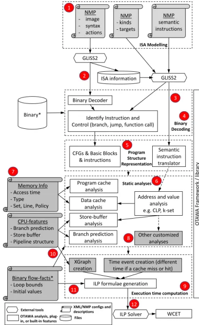
Figure 1 shows the steps to perform a WCET analysis for a given platform. In this figure, the activities required to tailor OTAWA for a new target are shaded in grey. The global process involve two activities and two parties: a non-recurrent but relatively heavy activity (see Section IV) for the developer who describes the ISA (Instruction Set Architecture), constructs the static analyses, and provides the configurations of the platform; a recurrent but light activity for the user, who provides the “facts” about programs to be analysed, such as the maximum number of iterations for loops, and uses OTAWA to computes their WCETs. Let’s detail the different steps. In 1 , the characteristics of the instructions are defined using the NMP format [5]. In addition, the developer provides information useful for OTAWA: types of instructions (e.g. an ALU instruction, a branch instruction, etc.), targets of branches, behaviours using semantic instructions [6], etc. This information allows the subsequent static analyses to be independent from the architecture. The NMP files are processed by the GLISS [7] tool to create the binary decoder 2 and the semantic instruction translator 3 .
The WCET estimation performed by OTAWA begins with the binary decoding 4 and program structure representation 5 phases in which the CFGs (Control-Flow Graphs), the BB (Basic Blocks), and each individual instructions are built.
The core activities are those concerning the static analyses 6 which are performed to determine the impact of the various processor features, such as the program/data caches, on the estimating WCET. To support a new processor target, the developers can either configure the existing analyses, e.g. by specifying the policy of the data-cache 7 , or create customised analyses 8 .
The results of the analyses are used by the execution time computation 9 which relies on the eXecution Graph (XGraph) model, which captures the time taken by each instruction in the processor pipeline. XGraph, first proposed in [8], has been extended and refined to support the tracking of internal resources in [9]. The creation of the XGraph requires the developer to provide information about the pipeline 10 . The impacts of the timings of both the software and the processor features, obtained from the static analyses, are captured in the XGraph using time events. The XGraph creation is further described in section III-F. Next, the possible execution times for each BB, along with the different configurations of time events are encoded in an Integer Linear Programming (ILP) problem. Constraints such as the maximum number of iterations for a loop and the initial values of registers/memory locations are provided by the user 11 to further refine the ILP problem. The ILP problem is solved so as to maximise the execution time 12 . The solution is the WCET estimation.
2See https://www.absint.com. 3See https://team.inria.fr/pacap/software/heptane.
Semantic instruction
translator
Address and value analysis e.g. CLP, k-set O TA W A Fr am ew or k / libr ar y GLISS2 Binary Decoder GLISS2 Binary* ISA information NMP semantic instructions NMP - kinds - targets NMP - image - syntax - actions 11
CFGs & Basic Blocks & instructions
Identify Instruction and Control (branch, jump, function call)
ISA Modelling
Memory Info - Access time - Type - Set, Line, Policy
Program cache analysis Data cache analysis CPU-features - Branch prediction - Store buffer - Pipeline structure Store-buffer analysis Binary flow-facts* - Loop bounds - Initial values Branch prediction analysis
Time event creation (different time if a cache miss or hit) XGraph
creation
ILP formulae generation
ILP Solver WCET
Program Structure Representation Binary Decoding Other customized analyses Static analyses
Execution time computation
1 2 3 4 5 6 7 8 9 10 11 12
External tools XML/NMP configs and descriptions OTAWA analysis,
plug-in, or built-in features Files
Fig. 1: The work-flow of computing WCET in OTAWA
B. The target processor: Infineon TC275
Our target processor is the Aurix TC275, a multi-core pro-cessor developed by Infineon mainly for the automotive market, and designed to minimise inter-core interferences. The TC275 is one of the target processors of the industrial partners in our project4. It is also the target of other research activities focused
on interference analysis [10] and automatic parallelisation. The overall architecture of the TC275 is given in figure 2. The TC275 embeds three cores: one E-core (for Efficiency) and two P-cores (for Performance). E- and P-cores implement the same Tricore 1.6 architecture [11] but with different features such as different sizes of caches, but also different pipeline architectures: while the E-core is a scalar processor, the P-core is a super-scalar processor equipped with a program-fetch-FIFO to enhance its
4Project “CAPHCA” (Critical Applications on Predictable High-Performance
Computing Architecture) is an on-going project at the Institut de Recherche Technologique (IRT) Saint-Exup´ery, Toulouse, France.
performance. The architecture of the E-core and P-core pipelines are given in figure 3
(peripherals connected to the SPB are not represented)
Fig. 2: The internal architecture of the TC275 (from [11]).
III. TAILORINGOTAWAFOR THETC275
Section II has introduced the main steps of the WCET anal-ysis process. Here, we detail the steps involved specifically in the tailoring process (those shaded in grey in Figure 1), namely: the modelling of the instruction set architecture, the provision of the target-specific hardware parameters, the integration of the different analyses using the execution graph (XGraph), and the provision of the software-level data required by the analysis.
A. ISA modelling and translation to semantic instructions The ISA (Instruction Set Architecture) of the E-core and P-cores on TC275 both follow the Tricore 1.6 architecture, so only one ISA model is needed. The source of information about the ISA is the publicly available user manuals [12]. As an example, Listing 1 shows the NMP [5] model of the mov instruction in the SimNML language. The first line declares that mov operates on two data registers (of type reg d) named c and b. The second line describes the bit-level structure (or “image”) of the instruction, which is used to decode the instruction: the first 4 bits contain the ID of the register c, followed by the 8-bit value 0x1F, and so forth. An “X” indicates an unused bit. The third line describes the syntax of the operation in assembly code. The “kind” attribute gives characteristics of the instruction used by the static analysis, such as whether an instruction accesses a memory location, branches to a computed address, or perform an ALU operation. Finally, the action segment describes the behaviour of the instruction, which will be implemented by the Instruction Set Simulator (ISS) generated from the NMP description. In this example, the action assigns the value of
register b to register c. This segment is used to generate the binary decoder using GLISS2, as mentioned in section II-A.
Listing 1: NMP model for a mov instruction
op mov reg ( c : r e g d , b : r e g d ) i m a g e = f o r m a t (”%4 b %8b XXXX %4b XXXX %8b ” , c . image , 0 x1F , b . image , 0x0B ) s y n t a x = f o r m a t ( ” mov %s , %s ” , c . s y n t a x , b . s y n t a x ) k i n d = 0 x 1 0 0 0 0 0 0 0 a c t i o n = { c = b ; }
To make static analysis as independent as possible from the target platform, OTAWA translates each instruction into a set of more primitive semantic instructions [6], as shown in Listing 2. The semantics of the mov instruction is expressed using a SET semantic instruction which states that data-register c shall get the value of data-register b.
Listing 2: Semantic instructions for the MOV instruction
e x t e n d mov reg
sem = { SET (D( c . i ) , D( b . i ) ) ; }
This activity of modelling the ISA and creating the semantic instructions, while tedious and error-prone, can be achieved in a systematic manner on the basis of the available documentation. The verification process of this model is presented in [3].
B. Hardware configuration
Step 7 of the WCET analyser development workflow re-quires information about the hardware features. This includes the configuration of the program and data caches, and the characteristics (e.g. access times) of the device’s memories and peripherals. For instance, listing 3 shows the configuration of the program cache (or icache in OTAWA’s convention) of CPU0. The size of the cache-line (also called block), the number of ways (or sets), and the number of lines (rows) are also specified. This information is retrieved from the TC275’s user-manual [11]. The data-cache (dcache) is configured in the same way.
Listing 3: The description of cache
<c a c h e −c o n f i g>
<i c a c h e> <!−− 8 KB −−>
< b l o c k b i t s>5</ b l o c k b i t s> <!−− 32B l i n e −−> <w a y b i t s>1</ w a y b i t s> <!−− 2 ways −−> <r o w b i t s>7</ r o w b i t s> <!−− 128 s e t s −−> </ i c a c h e><d c a c h e> . . . </ d c a c h e>
</ c a c h e −c o n f i g>
Memory accesses, such as the instructions fetching and data accesses from/to local memories or peripherals usually con-tribute substantially to execution times. Therefore, the accuracy and the precision of the WCET estimations strongly depend on the model of the memory structure.
As shown on Figure 2, each CPU of the TC275 is fitted with a scratch-pad memory (SPR) for both program (PSPR) and data (DSPR). The CPUs have also access to a set of shared memories via a cross-bar bus (SRI): program/data flash (PFlash/DFlash) located in the Program Memory Unit (PMU), SRAM located in the Local Memory Unit (LMU). Memory access latencies
depend on whether accesses are local (in DSPR or PSPR) or via the SRI where they are submitted to the bus arbitration policy. The range of memory access latencies is very large. For example, a load instruction (e.g. ld.w) can result an execution time from 1 cycle (local access to DSPR) to 64 cycles (remote access to DFlash).
Listing 4: The description of a memory component
<memory> <b a n k>
<name>PFLASH0</ name>
<a d d r e s s>0 x80000000</ a d d r e s s>
< s i z e>0 x01000000</ s i z e> <!−− 2 MBytes /−−> <l a t e n c y>13</ l a t e n c y>
< w r i t a b l e> f a l s e</ w r i t a b l e> <c a c h e a b l e> t r u e</ c a c h e a b l e> </ ba nk><b a n k> . . . </ ba nk> </ memory>
Memories and memory-mapped peripherals are specified as shown in Listing 4 (PFLASH0 on PMU). Note that information about this component is scattered throughout the documentation, and in various formats. For instance, cache-ability is found in the user-manuals (section 3.2 of [11] and section 8.2.1 of [12]), information about the PMU are found in section 10 of [11], etc. Access times, which are crucial to the WCET computation, is specified with a formula depending on the value of various bits of the FCON (Flash CONfiguration) register. In the latter case, we have confirmed the values obtained from the formula by performing measurements on the actual physical target, and cross-checked these values with those obtained from other sources [13]. Finally, obtaining all the data necessary to configure the hardware model require both experience and significant efforts. F2 Pre-decode Integer F I F O (6) P-Core
Fetch Decode EX1
E-Core Decode EX1 EX2
Pre-decode LD/ST Pre-decode Loop Store Buffer (6) Store Buffer (4) F1 EX1 Integer EX2 Integer EX1 LD/ST EX2 LD/ST EX1 Loop EX2 Loop Decode Integer Decode LD/ST Decode Loop
Fig. 3: The pipeline model of the cores in TC275. Information about the processor pipeline is also required. The pipeline structures of the E-core and P-cores of TC275 are shown in Figure 3. The corresponding XML description of the P-core’s pipeline stages is shown in Listing 5.
“FETCH” denotes the stage where instructions entering the processor pipeline (line 1). “LAZY” represents a pipeline stage where instructions are held for a constant duration of 1 cycle (line 2–4). In this case, the 2nd stage of the fetching (the F2 stage), the pre-decoding (PD) stage, and the decoding (DE) stage fall into this category. “EXEC” denotes an execution stage (line 5), attributes of this stage are further specified, such as the in-order execution (line 6). The execution stage is further refined into the loop (EXE L), the integer (EXE I), and the
load/store (LS) memory (EXE M) Functional Units, FUs (lines 8–13). The latency of 2 for the FUs indicates that there are 2 execution phases for each pipeline (EX1 and EX2). Lines 11 indicates that the EXE M pipeline involves with accessing the memories/peripherals, while the access occurs at the second execution phase (denoted by 1 in line 12, where 0 indicates the first execution phase) of the EXE M pipeline.
Listing 5: The description of the P-Core’s pipeline
1 <s t a g e i d = ” F1 ”><t y p e>FETCH</ t y p e></ s t a g e> 2 <s t a g e i d = ” F2 ”><t y p e>LAZY</ t y p e></ s t a g e> 3 <s t a g e i d = ”PD”><t y p e>LAZY</ t y p e></ s t a g e> 4 <s t a g e i d = ”DE”><t y p e>LAZY</ t y p e></ s t a g e> 5 <s t a g e i d = ”EXE”><t y p e>EXEC</ t y p e>
6 <o r d e r e d> t r u e</ o r d e r e d> 7 <!−− The p i p e l i n e s −−>
8 <f u i d = ”EXE L”><l a t e n c y>2</ l a t e n c y></ f u> 9 <f u i d = ” EXE I ”><l a t e n c y>2</ l a t e n c y></ f u> 10 <f u i d = ”EXE M”><l a t e n c y>2</ l a t e n c y> 11 <mem> t r u e</ mem>
12 <mem stage>1</ mem stage> 13 </ f u>
14 <d i s p a t c h>
15 <t y p e>0 x80000000</ t y p e><f u r e f = ”EXE L” /> 16 <t y p e>0 x40000000</ t y p e><f u r e f = ”EXE M” /> 17 <t y p e>0 x10000000</ t y p e><f u r e f = ” EXE I ” /> 18 </ d i s p a t c h>
19 </ s t a g e>
20 <s t a g e i d = ”CM”><t y p e>COMMIT</ t y p e></ s t a g e> 21 <q u e u e>
22 <name>FETCH QUEUE</ name> 23 < s i z e>6</ s i z e>
24 <i n p u t r e f = ” F2 ” /> 25 <o u t p u t r e f = ”PD” /> 26 </ q u e u e>
OTAWA uses instruction “kind” (see Listing 1) to determine to which destination pipeline the instruction must be dispatched. In the example, the mov instruction is of the kind 0x1000000, which indicates that it must be executed by the EXE I (the integer pipeline).
Finally the CM stage (line 20) of the type “COMMIT” determines the completion of an instruction. Thus, the execution time of instructions is estimated by computing the difference between the commit times of two successive instructions.
The last element of the model, FETCH QUEUE, describes the FIFO used to store the fetched instructions before they are dispatched to the appropriate execution pipelines.
Information about the pipeline have been obtained from various sources, including the user manual [11] (for the fetch and execution organisations), and publications [14] (for pipeline stages). The actual size of the Fetch-FIFO has been inferred from a series of experiments performed on the actual processor. Overall, information required to feed the analysis model has been obtained by browsing formal documentation (user’s manual), skimming through various application notes and pre-sentations, and experimenting on the actual target. It is worth noting that a unique source (document, chapter in the data-sheet or user’s manual) providing the structural and behavioural data required to estimate execution times would significantly simplify the WCET analysis.
C. Developing or reusing static analyses
In the simplest scenario, a processor fetches an instruction without delay. The fetched instruction is then processed through the pipeline with each stage taking one cycle. In this simple case, accesses to memory and peripherals also take one cycle. Things are obviously much more complicated in reality.
On the TC275, due to size constraints, the application code may not fit completely in the local PSPR, and must be stored in the PFlash. The PFlash access time varies from 5 to 14 cycles, depending on the state of the buffers located within the PMU (where the PFlash resides). In order to reduce the impact of this latency on performance, each P-Cores is equipped with a pre-fetch buffer within its fetch unit. In the best scenario, the pre-fetching completely masks the PFlash latency. However, when considering WCET estimations, it is essential to capture the worst-case scenario, that is, in this case, to ignore the presence of the instruction pre-fetching and systematically take the worst access-time of PFlash. The resulting over-estimation is huge (to 14 times, by comparing worst case of 14 cycles to access PFlash and 1 cycle due to pre-fetching). This over-estimation is safe, but it may be also so pessimistic that it leads either to an under-utilization of the platform (i.e., the cautious software architect allocates time budgets much larger than what would actually be needed), or to a failure of the schedulability tests (although the system may well be actually schedulable). Therefore, in order to improve precision, reduce pessimism, and keep a safe estimation, modelling the pre-fetching mechanism was considered necessary. Similarly, other processor features such as instruction/data caches, store-buffers, and super-scalar execution – which also have a large potential effects on execution times –, were added to the model.
Listing 6: Analyses for the E-core
1 < s c r i p t>
2 <s t e p r e q u i r e = ” t r i c o r e 1 6 : : B r a n c h P r e d T C 1 6 E ” /> 3 <s t e p r e q u i r e = ” otawa::ICACHE CATEGORY2 FEATURE ” /> 4 <s t e p r e q u i r e = ” otawa::ICACHE ONLY CONSTRAINT2 ” /> 5 <s t e p r e q u i r e = ” otawa::clp::CLP ANALYSIS FEATURE ” /> 6 <s t e p r e q u i r e = ” o t a w a : : d c a c h e : : C L P B l o c k B u i l d e r ” /> 7 <s t e p r e q u i r e = ” o t a w a : : d c a c h e : : A C S M u s t P e r s B u i l d ” /> 8 <s t e p r e q u i r e = ” o t a w a : : d c a c h e : : A C S M a y B u i l d e r ” /> 9 <s t e p r e q u i r e = ” o t a w a : : d c a c h e : : C A T B u i l d e r ” /> 10 <s t e p r e q u i r e = ” o t a w a : : d c a c h e : : C a t C o n s t r a i n t B u i l d ” /> 11 <s t e p r e q u i r e = ” t r i c o r e 1 6 : : B B T i m e r T C 1 6 E ”> 12 <s t e p r e q u i r e = ” otawa::ipet::WCET FEATURE ” /> 13 </ s c r i p t>
Modelling all features that have (or may have) a significant impact on execution times requires a significant effort. Hope-fully, some features are common in one processor architecture to another, such as the LRU (Least Recently Used) policy used in the caches, for instance. OTAWA provides a collection of static analyses (“built-ins”) developed over time to model the supported processor architectures. In the best case, the user can simply pick up one of these components to build his own model. In the other cases, i.e., when some processor features are specific, one has to develop its own analysis component, which then becomes part of the collection.
Listing 6 gives the sequence of analyses used for the E-Core (the configuration for the P-Core is similar). Within this list, analyses
prefixed with ”otawa::” are OTAWA built-ins, while the ones prefixed with ”tricore16::” have been developed specifically for the TC275.
Selecting the necessary static analyses requires a good expe-rience and understanding of the target processor. The following section describes how this choice has been done for the TC275 E-core.
D. Static analyses for instruction fetching
To analyse instruction fetching, one must consider if the processor is featured with (1) branch prediction, (2) instruction cache(s), and (3) any other mechanism such as pre-fetching. For the E-core, branch prediction is static and depends on the type of the branch instruction being executed. So we use a dedicated analyses shown in line 2 on Listing 6.
The TC275 cores uses a standard LRU policy for its in-struction cache, so we use the OTAWA built-in analysis, as shown in lines 3 and 4. The configuration of this analysis is given in the Listing 3. The static analyses on line 3 determines if an instruction cache-miss must/may/never happens at any given program point. That is, the analysis is made for all the instructions on the instruction-cache boundary. The analysis on line 4 uses the previous result to check if an instruction cache-miss can happen on a given instruction. In that case, different scenarios will be explored to ensure that the static analysis covers all possible cases, i.e. different combinations of cache-hit and -miss to ensure that timing anomalies [1] are taken into account. Otherwise, the fetching of that instruction will never have a timing penalties.
E. CLP Analysis: value and address analysis
As shown on Figure 1, the program structure and the in-struction sequences are computed before the static analyses are performed (step 5, CFGs, basic blocks, instruction). The addresses of fetch accesses are known at that time, but the addresses of data accesses are much more complicated to obtain since they usually depend on the behaviour of the application. However, knowing addresses of data accesses is crucial, as they convey very important information for the WCET estimation:
1) The memory component targeted by the access: access time on local DSPR and DFlash show huge differences (around 60 times), so considering that all data-accesses with unknown target addresses are to the DFlash will lead to huge over-estimation;
2) Whether the target address is cache-able or not: if cache-able this will affect the state of the cache and hence the later cache-able accesses;
3) The necessity of finding dynamic branch targets: for example, the target of switch-case statements are evaluated based on the value of the dependant data.
We use CLP analysis [6] as the main value-and-address analysis in OTAWA, as shown in line 5 of Listing 6. The analysis relies on abstract interpretation [15]. It provides estimated abstract values of the TC275 registers (data registers, address registers, program counter, and other registers for context sav-ings), and memory locations, at all program points. This analysis
also provides the target addresses of memory accesses since all memory access instructions in E/P-cores use address registers. The other static analyses, such as data-cache analysis depend on CLP analysis.
The data representation of the CLP analysis is in the form of start, step, count as described in [16]. For example, value 0x100, 0x2, 0x20 describes a set of 21 different values: 0x100+0x2*i, with i in 0,1,. . . ,20. Two special values inherited from the abstract interpretation are Bottom (⊥) and Top (>), which are used to denote un-initialized and unknown/any values, respec-tively. Access registers/memories with un-initialized values only happen on incorrect programs, which is out of the scope of this paper. The Top value, due to widening and joining operations from the abstract interpretation, can propagate and cause over-estimation on WCET. As one cannot tell the value of an address register, the data access based on that will refer to the access to the DFlash (the worst case).
Listing 7: The invariant to the CLP analysis
1 <r e g − i n i t name= ” A10 ” v a l u e = ” 0 x 7 0 0 1 9 6 0 0 ” /> 2 <r e g − i n i t name= ” PCXI ” v a l u e = ” 0 x70019C00 ” /> 3 <mem− i n i t a d d r e s s = ” 0 xD0000040 ” v a l u e = ” 0 x70019C00 ” /> 4 < s t a t e a d d r e s s = ” 0 x 8 0 0 0 0 4 0 2 ”> 5 <r e g name= ”A4” s t a r t = ” 0 x600 ” s t e p = ” 1 ” c o u n t = ” 400 ” /> 6 <mem a d d r e s s = ” 0 xD0000080 ” v a l u e = ” 0 x70019C00 ” /> 7 </ s t a t e>
In order to avoid this pessimism, we have provided the user with the capability to give additional information (initial values and invariants) to support the analysis, as shown in Listing 7.
Invariants enables the users to define the initial values of the registers/memories, i.e., values that cannot be inferred from the program analysis. For example, the value of the PSW (program status word) register is set to 0x00000B80. This is also useful when the WCET estimation is performed for a part of a program, i.e. a task among the whole application, where the associated register/memory values are pre-defined, e.g. the stack pointer register (A10 in Tricore) and the context register (PCXI), whose initial values are defined in lines 1 and 2 using the reg-init clause respectively.
While the initial values are used at the beginning of the CLP analysis, it is also possible to introduce invariants at a given program point. For example, when a register/memory value is set to Top (which affects the results of the WCET estimation), one can inject a snapshot of the state, which always stands, i.e. the value given satisfies at all possible scenarios on the associated program point, through the use of the state clause, as shown in lines 4–7. The invariant state is associated with a program point by providing the instruction address (line 4). The values of registers and memories are assigned under the scope of the corresponding invariant state, as lines 5 and 6, where in line 5 the register A4 can cover of 401 possible values while in line 6 the value is fixed to a constant.
It is extremely important to note that an incorrect initial value or invariant can completely ruin the safety of the analysis. Ensuring the correctness of those values are strictly under the responsibility of the user.
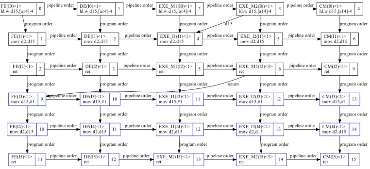
Fig. 4: XGraph of an instruction sequence for E-core.
F. Analyses associated with the data cache
As the CLP analysis provides values of registers/memory locations, it is possible to determine the target addresses of memory-accesses (arguments of the all variants of ld (load) and st (store) instructions. This is achieved by the CLPBlock-Builder analysis (line 6 of Listing 6), as the first step of the data-cache analysis. The state of the data cache is determined by each data-access whose target address (obtained from the CLP analysis) is identified as cache-able. If the target address for a given data-access is unknown, i.e. Top-valued (>), the data-cache analysis considers that the access can possibly affect all the cache-lines. Such assumption is safe but reduces the precision of the analysis. One way to improve the precision is to provide state information (initial and invariant) when performing the CLP analysis.
Similar to instruction-cache analysis, for each possible data-access associated with data-cache, the data-cache analyses de-termines if a data-cache miss must/may/never happen, through the uses of ACS (abstract cache state) analyses (lines 7–9 in Listing 6). Similar to line 4, line 10 creates scenarios which cover all possible cases to evaluate the execution times for possible data-cache misses.
Once all the previous analyses are completed, OTAWA creates XGraphs to compute the execution time of the instruction sequences. This is detailed in the next section.
G. XGraph: timings within instructions and pipeline stages Figure 4 shows the CFGs of the binary search program of the M¨alardalen benchmark [17]. The CFG at the left, which is the main function, calls the binary search function at BB3. On the right-hand side, the search function terminates at BB8, and returns to main function’s BB2. The execution time of each BB is first computed and is used to compute the overall WCET of the target program. To compute a BB’s execution time, OTAWA considers the state of the processor as well as
FE(I0)<1>
ld.w d15,[a14]-4 0 DE(I0)<1>ld.w d15,[a14]-4 1 pipeline order FE(I1)<1> mov d2,d15 1 program order EXE_M1(I0)<1> ld.w d15,[a14]-4 2 pipeline order DE(I1)<1> mov d2,d15 2 program order EXE_M2(I0)<1> ld.w d15,[a14]-4 3 pipeline order EXE_I1(I1)<1> mov d2,d15 4 program order CM(I0)<1> ld.w d15,[a14]-4 4 pipeline order d15 EXE_I2(I1)<1> mov d2,d15 5 program order CM(I1)<1> mov d2,d15 6 program order pipeline order FE(I2)<1> ret 2 program order pipeline order DE(I2)<1> ret 3 program order pipeline order EXE_M1(I2)<1> ret 5 program order pipeline order EXE_M2(I2)<3> ret 6 program order CM(I2)<1> ret 9 program order pipeline order FE(I3)<1> mov d15,#1 9 program order pipeline order DE(I3)<1> mov d15,#1 10 program order pipeline order EXE_I1(I3)<1> mov d15,#1 11 program order pipeline order return EXE_I2(I3)<1> mov d15,#1 12 program order CM(I3)<1> mov d15,#1 13 program order pipeline order FE(I4)<1> mov d2,d15 10 program order pipeline order DE(I4)<1> mov d2,d15 11 program order pipeline order EXE_I1(I4)<1> mov d2,d15 12 program order pipeline order EXE_I2(I4)<1> mov d2,d15 13 program order CM(I4)<1> mov d2,d15 14 program order pipeline order FE(I5)<1> ret 11 program order pipeline order DE(I5)<1> ret 12 program order pipeline order EXE_M1(I5)<1> ret 13 program order pipeline order EXE_M2(I5)<3> ret 14 program order CM(I5)<1> ret 15 program order
pipeline order pipeline order pipeline order pipeline order
Fig. 5: XGraph of an instruction sequence for E-core.
the context of the program execution, therefore the predecessor BBs are also taken into account. For example, to compute the execution time of BB2 of the main function (at the left, with address 0x8000080A), its predecessor, BB8 at the right (with the address 0x800007F8) is included to create a XGraph, shown as Figure 5, for its execution on the E-core (CPU0) on TC275. We call BB2 the Body BB (the 3 rows in blue at the bottom of the XGraph) and BB8 the Prefix BB (the 3 rows in black at the top of the XGraph), and the instructions of the two BBs form an instruction sequence.
In this example, all the instructions are located in the local PSPR and all the data are located in the local DSPR, so that the memory access times are included in the associated pipeline stages (Fetch stage for the instruction fetch and the second execution stage for memory access). An XGraph consists of the following elements:
1) Pipeline stages: The horizontal nodes correspond to the movement of an instruction within the pipeline stages of the processor. In this example, E-core consists of 4 pipeline stages, as illustrated in Figure 3: the Fetch (FE), the Decode (DE), and two execution stages for each pipelines, i.e. EXE M1 and EXE M2 for the memory load-store pipeline, and EXE I1 and EXE I2 for the integer pipeline. An extra stage, CM (which stands for a Commit stage, as shown in line 20 of Listing 5), is used to indicate the end of executing the instruction. 2) Instruction sequence: The XGraph is used to compute
the time taken to execute a set of instructions. The vertical nodes are used to present individual instruction in the sequence. Each node has a name in the form of Stage(Instruction), e.g. DE(I1) means the second
instruc-tion at the Decoding stage.
3) Duration for each node: Each node is associated with a cost, which is the time taken for the instruction to complete a given stage. The cost is indicated in the <>, e.g. EXE M2(I2)<3>indicates that it requires 3 cycles for instruction 2 to complete the second execution stage. 4) The edges between the nodes: The edges between nodes represent the relationship between the connected nodes. A solid line gives the ”after” relation. Since the TC275 executes instruction in order, each instruction is connected to the previous instruction with a solid line. The dependencies between data are also expressed with the same line. For example, the first instruction (I0) loads the value from the memory to the data register d15. The next instruction (I1), which uses d15 at the first execution stage (EXE I1), must wait until the data is ready, i.e., at the end of the second execution stage (EXE M2) of I0. The solid line labelled “d15” indicates this dependency. Similarly, the edge between EXE M2(I2) to FE(I3) shows that the execution of the instruction ret (return from current call), requires 4 cycles to complete (1 cycle for the first execution phase, and 3 cycles for the rest) by restoring the context registers (including the program counter, PC) from local DSPR (operations are defined in [12]). The fetching process of I3 can only begin after executing I2 hence the solid line in between. The other kind of edge, drawn with dashes, denotes the “as-early-as” relationship between nodes. This is useful to describe, for instance, that the execution stages of integer- and memory/LS- pipelines can start at the same time (on the P-Core).
F1(I6)<1>
st.w d15,[a14]-8 13 F2(I6)<1>st.w d15,[a14]-8 14 pipeline order F1(I7)<14> mov d15,#-1 14 line PD(I6)<1> st.w d15,[a14]-8 19 pipeline order F2(I7)<1> mov d15,#-1 28 program order DE(I6)<1> st.w d15,[a14]-8 20 pipeline order PD(I7)<1> mov d15,#-1 29 program order EXE_M1(I6)<1> st.w d15,[a14]-8 21 pipeline order DE(I7)<1> mov d15,#-1 30 program order EXE_M2(I6)<1> st.w d15,[a14]-8 22 pipeline order EXE_I1(I7)<1> mov d15,#-1 31 program order CM(I6)<1> st.w d15,[a14]-8 23 pipeline order EXE_I2(I7)<1> mov d15,#-1 32 program order CM(I7)<1> mov d15,#-1 33 program order pipeline order F1(I8)<1> st.w d15,[a14]-4 14 intra F1(I10)<14> ld.w d15,[a14]-12 31 cache pipeline order F2(I8)<1> st.w d15,[a14]-4 28 program order pipeline order PD(I8)<1> st.w d15,[a14]-4 29 superscalar pipeline order DE(I8)<1> st.w d15,[a14]-4 30 superscalar pipeline order EXE_M1(I8)<1> st.w d15,[a14]-4 31 superscalar EXE_M2(I8)<1> st.w d15,[a14]-4 32 d15 pipeline order superscalar CM(I8)<1> st.w d15,[a14]-4 33 superscalar pipeline order F1(I9)<1> j 800007ec 14 intra pipeline order F2(I9)<1> j 800007ec 28 program order pipeline order PD(I9)<1> j 800007ec 30 program order pipeline order DE(I9)<1> j 800007ec 31 program order pipeline order EXE_M1(I9)<0> j 800007ec 32 program order pipeline order EXE_M2(I9)<1> j 800007ec 33 program order CM(I9)<1> j 800007ec 34 program order pipeline order line pipeline order F2(I10)<1> ld.w d15,[a14]-12 45 program order pipeline order branch prediction PD(I10)<1> ld.w d15,[a14]-12 46 pipeline order pipeline order DE(I10)<1> ld.w d15,[a14]-12 47 pipeline order pipeline order EXE_M1(I10)<1> ld.w d15,[a14]-12 48 pipeline order pipeline order EXE_M2(I10)<4> ld.w d15,[a14]-12 49 pipeline order CM(I10)<1> ld.w d15,[a14]-12 53 pipeline order pipeline order F1(I11)<1> ld.w d2,[a14]-8 31 intra pipeline order F2(I11)<1> ld.w d2,[a14]-8 45 program order pipeline order PD(I11)<1> ld.w d2,[a14]-8 47 program order pipeline order DE(I11)<1> ld.w d2,[a14]-8 48 program order pipeline order EXE_M1(I11)<1> ld.w d2,[a14]-8 49 program order pipeline order EXE_M2(I11)<4> ld.w d2,[a14]-8 53 program order EXE_M1(I12)<1> jge d2, d15, 80000768 57 d15 CM(I11)<1>ld.w d2,[a14]-8 57 program order pipeline order F1(I12)<1> jge d2, d15, 80000768 31 intra pipeline order F2(I12)<1> jge d2, d15, 80000768 45 program order pipeline order PD(I12)<1> jge d2, d15, 80000768 48 program order pipeline order DE(I12)<1> jge d2, d15, 80000768 49 program order pipeline order program order pipeline order d2 EXE_M2(I12)<1> jge d2, d15, 80000768 58 program order CM(I12)<1> jge d2, d15, 80000768 59 program order pipeline order pipeline order pipeline order pipeline order pipeline order pipeline order
Fig. 6: XGraph of an instruction sequence for P-core exercising super-scalar effect and cache-misses
number next to the node indicates the arrival time of the node at the latest. For example, node FE(I3) has two incoming edges, one from FE(I2) the fetching node of the previous instruction with the arrival time of 2, and another one from EXE M2(I2) with the arrival time of 6. The arrival time of a node is the arrival time of the previous node plus its duration, e.g. the arrival time of FE(I2) to FE(I3) is 2+1=3, while EXE M2(I2) to FE(I3) is 6+3=9 which is the maximum outcome. The execution time of a sequence of instructions is the end time of the Body BB, minus the end time of the Prefix BB, i.e. (15+1) -(9+1) = 6 cycles.
H. Integration with the XGraph
Figure 6 illustrates a XGraph of the partial instruction se-quence of BB1 and BB2 for the binary search function (on the right of the Figure 4) running on the P-core (CPU1/CPU2). We use this XGraph to illustrate the effects of the super-scalar pipeline (P-core) and the instruction cache-misses. The XGraph shows 7 pipeline stages (in contrast to 5 stages for E-core) as described in Figure 3.
The super-scalar effect of the P-cores allows two instructions of two different pipelines (integer- and memory/ls- pipelines) to be dispatched and executed at the same time, given that the instruction order is an integer-pipeline instruction followed by a memory/ls-pipeline instruction. This information has been obtained from the user manual of an older version of Tricore [18]. We had confirmed that the TC275 still implements the same behaviour by observing the performance counters [11], which give the number of dispatches due to super-scalar effect. This feature is captured in XGraph using the dashed edges between the nodes. For example, in Figure 6, the instructions I7 (move) and I8 (store) satisfy the requirement of super-scalar execution. Their associated nodes (after the stage F2, which dispatches the instructions), are linked with dashed edges. Note that the arrival time of I7 and I8 stages (PD, DE, E1, and E2)
are equal. The data dependency of the register d15 between the two instructions does not affect the super-scalar activities: at the end of E1 of I7, the result is ready, while during E1 of I8 the instruction was computing the target address to store and the result of d15 is used at the second execution stage.
The feature of the instruction cache is also captured. Instruc-tion in the same cached line are fetched simultaneously, hence the dashed edges between the Fetch stages of instructions I7, I8, and I9 (and also for the case of I10, I11, and I12). On the other hand, when the instruction-fetch crosses the cache-line, the penalty (fetch from the PFlash) will occur when cache misses. From the instruction-cache analysis, the nodes F1(I7) and F1(I10) “may” suffer from cache-misses. In this case, time events are created to enumerates all four possibilities (i.e. both miss, both hit, only I7 misses, and only I10 misses) to ensure the result is timing-anomaly-free. Figure 6 illustrates the situation “both miss” and hence a penalty of 14 cycles is given to both nodes (from 14 to 28, and from 31 to 45), as described in Section III-B.
I. Other enhancements to XGraph under developments The TC275 implements a store-buffer and an instruction FIFO to improve performances. The store-buffer is used to store the values of store instructions without having to wait for the actual access to memory. This is handled in a way similar to that described in [19]. The instruction FIFO buffer is used to accelerate the fetching of instructions. Its behaviour is still under investigation using the approach mentioned in Section IV.
For the moment, our analyser takes conservative assumptions: instead of benefiting from the store-buffer, writing to memory is done with the normal latency (e.g. 1 cycle for local DSPR and 8 cycles for SRAM in LMU) at the second execution stage of the memory/LS- pipeline. Without the acceleration of the instruction FIFO buffer, an instruction cache-miss will lead to a PFlash access. These assumptions introduce over-approximations but give safe results.
J. The flow-facts: The insights on the binary
At this point, the developer has enabled OTAWA to compute WCET for the TC275. Now, the user needs to provide additional information about the binary file under analysis, as shown in step (11) of Figure 1. This information is called the flow-facts. An example of a set of flow-facts is given in Listing 8.
As shown in Figure 4, the CFG at the right (for function binary search) have loops in its body, e.g. BB2-BB3-BB4-BB6-BB2, BB2-BB3-BB7-BB2-BB3-BB4-BB6-BB2, and so. Here, lines 2–7 give the facts for function binary search. Lines 3–6 give information about a loop: the header of the loop is located at offset 0xa0 (line 4) from the entry of the function, which is BB2 of the associated CFG (at address 0x800007ec); the bound of the loop is specified in line 5.
Listing 8: The flow-facts of a given programn
1 <f l o w f a c t s > 2 <f u n c t i o n l a b e l =” b i n a r y s e a r c h ”> 3 <l o o p l a b e l =” b i n a r y s e a r c h ” 4 o f f s e t =”0 xa0 ” <!−− 0 x 8 0 0 0 0 7 e c −−> 5 m a x c o u n t =”23”> 6 </ l o o p > 7 </ f u n c t i o n > 8 </ f l o w f a c t s > IV. EVALUATION
The evaluation of the effort to develop a static analyser is done according to two important criteria (for an industrial end-user): (i) the effort spent to tailor OTAWA to support the TC275, (ii) the accuracy and precision of the WCET estimatations computed by the tool.
A. Development effort
The total development effort requires around 17 weeks that can roughly be decomposed as follows:
• Creation and validation of the NMPs: 4 weeks
• Configuration of the processor features: 1 week (mostly
finding the pipeline structure)
• Customisation of the XGraph: 4 weeks • Customisation of static analyses: 8 weeks
Note that those developments have been done by one engineer with a very good knowledge of OTAWA, and is new to the TC275. The amount of the presented efforts have to be adapted to the user’s experiences and profile. In addition, the verification and validation efforts described in [3] took another 4 to 5 weeks. As shown in section II-A, the computation of execution times for each BB relies on a precise knowledge of the pipeline structure. Finding this structure is difficult without an appro-priate and reliable documentation. Hence we have performed a series of tests to infer the pipeline structure. This consists of fine tuning the CPUs such that: (1) setting the processor in a known state (including its pipeline) using, for instance, the
isync instructions to flush the CPU buffers, and (2) crafting instruction sequence carefully so that CPU features of interest will be exercised, e.g. creating instructions pairs which will trigger the super-scalar effect and measure the memory access times. This was a complex and tedious activity.
B. Accuracy and precision
The accuracy and the precision of the TC275 Static WCET analyser have been evaluated on a FOC (Field Oriented Control) brushless motor control application.
This application, as depicted on Figure 7, uses all the three cores: CPU0 and CPU1 are in charge of controlling two motors (one core per motor without communications between the motors); CPU2 is used to communicate with the rest of the system (in our case, the mission control system of a three-wheeled robot) via a CAN bus. The motor-control function is performed on a timer-triggered interrupt service request, which occurs every 50 us. However, the ISR is required to finish in 25 us due to the nature of the motor-position-sensing.
To compare the WCET estimations obtained using OTAWA with the actual execution times, we performed two kinds of mea-surements: firstly, using the non-intrusive performance counters built-in in each CPU, to obtain the cycle count and hence the execution time; secondly, using a GPIO-pin toggled at each iteration. In the latter case, the time elapsed was measured using an oscilloscope.
Rotor position from the encoder
3 phase PWMs generation 3 phase
signals Current sensing to
calculate the flux
ShieldBuddy TriCore TC275 Brushless DC motor
with encoder
Motor drivers based on STM L6230
CAN bus transceiver Communication for
speed and other info
Fig. 7: The FOC motor control setup.
For the FOC motor control, experiments have been performed to verify the compliance of a simple interrupt service routine to its timing requirement (25us). OTAWA’s estimation was 14.675us (2,935 cycles, for E-core, which is less effecient than the P-cores) to be compared with the value of around 12.24us obtained by measurements on the E-core with GPIOs available on the development board, resulting in an overestimation of about 20%.
V. RELATED WORKS
Several open-sourced WCET estimation tools based on ab-stract interpretation exist, but only a few are flexible enough to support the creation, reconfiguration, and extension of analyses by a end-user.
Heptane [20] implements multi-level cache analysis, but only supports a limited number of processor targets, and provides a limited set of built-in analyses. More generally, it has not been designed with the specific objective to facilitate the development
of new analysers for new architectures. Chronos [21] only supports SimpleScalar architecture although they implement a time calculation method very similar to OTAWA. Previous experiences showed that adding new analyses in Chronos is complex. Bound-T [22], which development is stopped now, provides several interesting data-flow analyses but it only sup-ports a few architecture and it is not aimed to be extended. TU-Bound [23] is mostly a set of independent tools that targets only one architecture (Infineon C167) and does not provide any facility for extension. SWEET [24], provided by the University of M¨alardalen, was the first to provide a generic time calculation method based on simulation but is now outdated. Yet, it still provides powerful data flow analyses independent of the archi-tecture thanks to the language ALF, an instruction behaviour description more powerful than OTAWA’s semantic instructions.
VI. CONCLUSIONS AND FUTURE WORKS
In this paper, we have shown the different steps to develop a custom WCET analyser using the OTAWA framework. We have demonstrated that this result can be achieved with a reasonable effort (i) for a real-time processor with limited complexity, and (ii) by a engineer having a good knowledge of the framework.
This paper points out the difficulties that have been encoun-tered during the design of the analyser, and how they have been circumvented. In particular, it shows that a significant effort has to be dedicated to collecting information from the docu-mentation and, sometimes, from the hardware itself. This effort could be significantly reduced by providing a section dedicated to temporal analysis in the user-manual/data-sheet.
Finally, this paper explains the trade-offs that have been done between the development efforts and the safety of the analysis, in order to reduce the over-estimation of the analysis to keep it useful.
In the future, we plan to combine Measurement-Based Prob-abilistic Timing Analysis (MBPTA, [25]) with static analysis in order to maximise the precision / modelling effort ratio. Our approach is aimed at guiding the design process of the analyser (i.e., determine the micro-architectural mechanism that can be abstracted or not, select the appropriate abstractions, etc.) on the basis of the WCET estimations obtained using MBPTA.
REFERENCES
[1] R. Wilhelm, T. Mitra, F. Mueller, I. Puaut, P. Puschner, J. Staschulat, P. Stenstr¨om, J. Engblom, A. Ermedahl, N. Holsti, S. Thesing, D. Whalley, G. Bernat, C. Ferdinand, and R. Heckmann, “The worst-case execution-time problem—overview of methods and survey of tools,” ACM Transac-tions on Embedded Computing Systems, vol. 7, no. 3, 2008.
[2] P. Cousot and R. Cousot, “Basic concept of abstract interpretation,” in Building the Information Society, R. Jacquard, Ed., Toulouse, France, Aug. 2004, pp. 359–366. [Online]. Available: http://www.di.ens.fr/
∼cousot/publications.www/Top4-Abst-Int-1-PC-RC.pdf
[3] W.-T. Sun, E. Jenn, and H. Cass´e, “Validating static WCET analysis: a method and its application,” in 19th International Workshop on Worst-Case Execution Time Analysis, 2019.
[4] H. Cass´e and P. Sainrat, “Otawa, a framework for experimenting wcet computations,” in ERTS’03, 2006.
[5] H. Herbegue, H. Cass´e, M. Filali, and C. Rochange, “Hardware archi-tecture specification and constraint-based wcet computation,” in 8th IEEE International Symposium on Industrial Embedded Systems, 2013. [6] H. Cass´e, F. Bir´ee, and P. Sainrat, “Multi-architecture value analysis for
machine code,” in 13th International Workshop on Worst-Case Execution Time Analysis, 2013.
[7] T. Ratsiambahotra, H. Cass´e, and P. Sainrat, “A versatile generator of instruction set simulators and disassemblers,” in 2009 International Symposium on Performance Evaluation of Computer & Telecommunication Systems, 2009.
[8] X. Li, A. Roychoudhury, and T. Mitra, “Modeling out-of-order processors for software timing analysis,” in 25th IEEE International Real-Time Systems Symposium (RTSS), 2004.
[9] C. Rochange and P. Sainrat, “A context-parameterized model for static analysis of execution times,” in Transactions on High-Performance Em-bedded Architectures and Compilers II. Springer, 2009.
[10] W.-T. Sun, E. Jenn, H. Cass´e, and T. Carle, “Automatic Identification of Timing Interferences on Multi-Core Processor in a Model-Based Approach,” in COMPAS, 2019, To be published.
[11] AURIX TC27x D-Step 32-Bit Single-Chip Microcontroller User’s Manual V2.2 2014-12.
[12] TriCoreTMV1.6 Microcontrollers User Manual (Volumes 1 and 2), V1.0.
[13] E. D´ıaz, E. Mezzetti, L. Kosmidis, J. Abella, and F. J. Cazorla, “Modelling multicore contention on the aurix tm tc27x,” in Proceedings of the 55th Annual Design Automation Conference (DAC), 2018.
[14] J. Harnisch, “Predictable hardware: The aurix microcontroller family,” in 13th Workshop on Worst-Case Execution Time Analysis, 2013.
[15] P. Cousot and R. Cousot, “Abstract interpretation: a unified lattice model for static analysis of programs by construction or approximation of fixpoints,” in Proceedings of the 4th ACM symposium on Principles of programming languages, 1977, pp. 238–252.
[16] R. Sen and Y. Srikant, “Executable analysis with circular linear pro-gressions,” Technical Report IISc-CSA-TR-2007-3, Computer Science and Automation Indian . . . , Tech. Rep., 2007.
[17] J. Gustafsson, A. Betts, A. Ermedahl, and B. Lisper, “The m¨alardalen wcet benchmarks: Past, present and future,” in 10th International Workshop on Worst-Case Execution Time Analysis, 2010.
[18] Tricore 1 Pipeline Behaviour and Instruction Execution Timing V1.1, 2004.
[19] W.-T. Sun, H. Cass´e, C. Rochange, H. Rihani, and C. Ma¨ıza, “Using execution graphs to model a prefetch and write buffers and its application to the Bostan MPPA,” in International Conference on Embedded Real Time Software and Systems (ERTS), 2018.
[20] D. Hardy, B. Rouxel, and I. Puaut, “The Heptane Static Worst-Case Execution Time Estimation Tool,” in 17th International Workshop on Worst-Case Execution Time Analysis, 2017.
[21] X. Li, Y. Liang, T. Mitra, and A. Roychoudhury, “Chronos: A timing analyzer for embedded software,” Science of Computer Programming, vol. 69, no. 1, pp. 56–67, 2007.
[22] N. Holsti and S. Saarinen, “Status of the bound-t wcet tool,” Space Systems Finland Ltd, 2002.
[23] A. Prantl, M. Schordan, and J. Knoop, “Tubound-a conceptually new tool for worst-case execution time analysis,” in WCET’08, 2008.
[24] B. Lisper, “Sweet – a tool for wcet flow analysis,” in Leveraging Applications of Formal Methods, Verification and Validation. Specialized Techniques and Applications, 2014.
[25] S. Edgar and A. Burns, “Statistical analysis of WCET for scheduling,” in Real-Time Systems Symposium, 2001.(RTSS 2001). Proceedings. 22nd IEEE. IEEE, 2001, pp. 215–224.
![Fig. 2: The internal architecture of the TC275 (from [11]).](https://thumb-eu.123doks.com/thumbv2/123doknet/14342258.499416/4.918.62.472.152.489/fig-internal-architecture-tc.webp)