HAL Id: hal-02545171
https://hal.archives-ouvertes.fr/hal-02545171
Submitted on 15 May 2020
HAL is a multi-disciplinary open access
archive for the deposit and dissemination of
sci-entific research documents, whether they are
pub-lished or not. The documents may come from
teaching and research institutions in France or
abroad, or from public or private research centers.
L’archive ouverte pluridisciplinaire HAL, est
destinée au dépôt et à la diffusion de documents
scientifiques de niveau recherche, publiés ou non,
émanant des établissements d’enseignement et de
recherche français ou étrangers, des laboratoires
publics ou privés.
Double side interconnection for vertical power
components based on macro and nano structured copper
interfaces and printed circuit board technologies
Bojan Djuric, Vincent Bley, Julien Morand, Olivier Dagut, Jean-Pascal
Cambronne, Stefan Mollov
To cite this version:
Bojan Djuric, Vincent Bley, Julien Morand, Olivier Dagut, Jean-Pascal Cambronne, et al.. Double side
interconnection for vertical power components based on macro and nano structured copper interfaces
and printed circuit board technologies. MiNaPAD, May 2019, Grenoble, France. �hal-02545171�
MiNaPAD 2019, May 22nd – 23rd , Grenoble; France
Double side interconnection for vertical power components based
on macro and nano structured copper interfaces and printed
circuit board technologies
Bojan D
JURIC12, Vincent B
LEY2, Julien M
ORAND1, Olivier D
AGUT2,
Jean-Pascal C
AMBRONNE2, Stefan M
OLLOV1Abstract
This paper describes a full copper Z-axis interconnection manufacturing for vertical power electronic components. The approach is a combination of a die embedding in a PCB and interconnections by macro post overlaid with nano wires, ensuring both electrical and thermal connection of the die.
Key words: Power electronics, power module, switch, active component, 3D integration, PCB-embedding, interconnection, electroplating, macro & nano.
1 Introduction
The power converters hold a central position in electrical engineering. The power ratings are increasing and the converters have to meet these needs in compact systems. For example, the current power density of commercialized power converters of 2 kW for photo-voltaic application is around 1 kW.l-1, whereas in the “Little Box Challenge”
organized by Google and IEEE densities reached 12 kW.l-1 [1-3]. This improvement is mainly explained
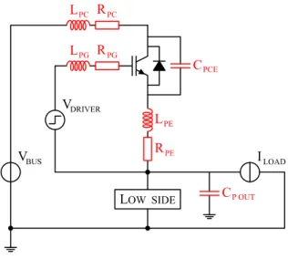
by using wide band-gap (WBG) semiconductor devices based on silicon carbide (SiC) and gallium nitride (GaN) materials that permit significantly higher switching frequencies. [4] However, the associated shorter switching times are only possible when all stray elements in the package (as shown in Figure 1) are minimized in order to take all the benefit of these new components [5].
The parasitic elements, and the package stray inductances in particular, are source of losses which reduce the efficiency and also cause less reliable operation and EMI noise. This is fundamentally difficult to achieve with the popular packages today using wire-bonds.
In some application, the WBG devices are expected to be able to work at higher temperature than silicon (Si) components. The junction temperature (Tj) of SiC components can be higher than 200°C in comparison of Si switches around 125°C. The package must endure high temperature and also resist the ensuing large temperature transitions.
Figure 1: Zoom on parasitic elements (red) of the high side switching cell induced by the packaging 2 Context
The PCB technology has the advantage of being a cost efficient and well-established process. There is a possibility of massive parallel manufacturing, fine pitch, thick copper used for heat and current transport, repeatable multilayer structures, etc. The embedding of power dies in PCB recently has solicited great interest. There are several kinds of proposed interconnections [1]. The greatest advantage of the technology for power device packaging is the strip-line approach of distributing current, bringing down the stray inductance close to the theoretical minimum.
1Mitsubishi Electric
R&D Centre Europe 1, allée de Beaulieu CS 10806
35 708 RENNES CEDEX 7 France
2Université de Toulouse;
UPS; INPT; LAPLACE; 118 rte de Narbonne – Bât. 3R3
CNRS; LAPLACE; F-31062 Toulouse France
The trend in PCB-embedding technology is to interconnect the components by using laser microvias [6]. The thermal conductivity of the PCB core is less than 1 W.m-1.K-1 for the polyimide material such a
kapton against 170 W.m-1.K-1 for aluminium nitride
for direct bonded copper (DBC) substrate. The micro-via approach suffers from the manufacturing limits imposed on their density, resulting in current and heat flux limitations.
This variation of the conveyed power through the converter is a source of temperature variations in the power assembly. Temperature gradient is present along the interconnections which, combined with different thermal expansion coefficient of each material, leads to crack at micro via and die interface and delamination over time. [7] These defects in the interconnection are affecting strongly the reliability of the converter, attributed to the cyclical stresses applied.
The proposed solution combines advanced PCB technologies and innovative interconnection solution without solder, based on electrolytic deposition of macro [8-9] and nano [10-11] structured interfaces, followed by thermo-compression. The assembly may thus be an elementary block for the design of power converters with high level of integration and reliability by means of a full copper and flexible interconnection [12-13] allowing for double-sided cooling. It is expected that the nano wires used as thermal and electrical die interface will be also more resistant to cyclical stresses.
3 Manufacturing process
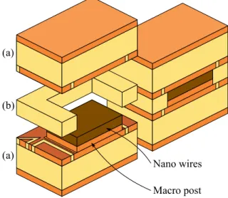
Our approach consists in sandwiching an opened core (in the cavities of which the power dies are inserted) between two PCBs having the macro-nano structured interfaces for the interconnections as shown in Figure 2. The PCBs and the core are assembled by stratification of a prepreg between each interface. This principle allows to limit the treatment steps on the component to be assembled.
The prototype assembly was manufactured with a silicon bare die with metallization consisting of 20 nm tungsten-titanium and 3 µm copper. The dimensions of the die are 7.2 × 4.2 mm² with 300 µm thickness, fully P-Boron doped and having a resistivity about 1 × 10⁻⁴ Ω.mm. The value of the
equivalent resistance is 100 µΩ.
The substrate used is an Arlon 35N PCB of 0.8 mm polyimide core overlaid of 105 µm copper layers. Electrically accessible by the two upper connectors, the central constricted area is used for the interconnection manufacturing. The remainder copper and ground planes are brown oxidized to increase the surface roughness and therefore the adhesion of the prepreg during final assembly
Figure 2: Cross section schematic of the assembly with macro and nano structured interfaces
pressing. There are two measuring tracks for characterization allowing kelvin measurement of the assembly (Figure 3). The through-holes are used to align the substrate on the different supports during the manufacturing process and to access the measuring pads of the second assembled substrate.
Figure 3: PCB substrate with constricted area, its connectors and kelvin measuring tracks
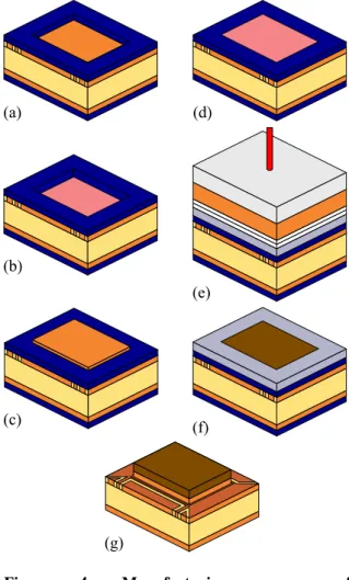
The macro-nano structured interface is composed of a macro post about 45 µm overlaid by nano wires around 55 µm length and 200 nm diameter. This is done in 7 manufacturing steps (Figure 4).
a. The PCB is first deoxidized by 10% sulfuric acid. Dry film (Dupont Riston T220 50 µm) is deposited to insulate all copper layers except the 2 connectors
Figure 4: Manufacturing process of interconnection on the PCB substrate
and a rectangle of 6.8 × 3.8 mm² on the central constricted area having rounded angles to avoid edge defects and to smooth copper deposition (Figure 5). b. On average, there is 7 µm of copper electro-etched during 45 minutes from the constriction track through the dry film opening. Thereafter the elecro-etching process, the anodic mud is cleaned from PCB’s copper surface.
c. After deoxidation of the anode and the PCB substrate, there is around 60 µm of copper electroplated during 7 hours on the electro-etched surface in order to have copper overflowing of the dry film opening.
d. The macro post is leveled to the dry film by carrying out the same electro-etching process of the step (b).
e. The Anodic Aluminium Oxide (AAO) membrane (Whatman Anodiscs Ø 47 0.2 µm) is applied onto the deoxidized macro post. The solution of 50% copper sulfate is spread all over. The membrane is overlaid of two cellulosic papers (Whatman Ashless Grade 41 Ø 60 20 µm). The electrolytic cell is maintained by pressure of the anode onto the assembly. Afterward, there is an hour of copper electroplating.
f. The cell is opened and the cellulosic papers are removed. The anode is put back without applying pressure. The membrane is caught by the short nano wires electroplated during the step (e). Therefore, the anode is distanced from the substrate in order to enhance the deposition by renewing of the solution. The AAO membrane is filled by electroplated copper during 6 hours deposition.
g. The dry film and AAO membrane are removed by 10% sodium hydroxide treatment at 45°C during 30 minutes.
The resulting metallic structure (Figure 5) has a thickness of 100 µm. The test coupon demonstrates a consistent and continuous nano-wire cover, which is important for good heat and current transport.
Figure 5: Digital microscope picture (x200) of the macro and nano structured interface
A SEM image of the deposited nano wires is shown in Figure 6. The nano wires are well separated (important to offer a flexible stress resistant interface) and have a high filling factor. Also, their length is within few µm, which we think is important for consistent impingement of the nano-forest to the die surface.
Figure 6: SEM acquisition (x10,000) of the nano wires 40° tilted top view
In the above process a pulsed current waveform was used for the electroplating and the electro-etching steps. It slows down the hydrogen and anodic mud production which are source of defects. That also allows to relax the ions on the PCB substrate and therefore it improves the homogeneity of copper deposition, especially for the nano structures manufacturing [14]. The current profile is chosen in accordance with the recommendation of the used equipment Bungard COMPACT A and its electrolytic solution Bungard CU400.
The core is made by stratification of Arlon 35N prepregs. Several different references are used to adjust the core thickness which decrees the electrical contact, especially the applied pressure on the nano wires and the die. The core is composed of two 106 prepregs, a 1080 prepreg and a 2116 one. The average of the reached thickness is 370 µm. Subsequently, the cavity is routed by CNC device (Bungard CCD/2/ATC) to host the active component. Sized for the die, the corners are shaped such as Mickey Mouse's ears. It avoids insertion defects due to the non-capability of the CNC tool to make straight angles.
All the stacked elements, which can be seen on Figure 2, are laminated by putting a 106 prepreg between each strata. Finally, the obtained distance between the two PCBs is 490 µm and approximates the 500 µm necessary to match the thickness of the top and bottom interconnections (each 100 µm) and the 300 µm die thickness.
4 Electrical characterization
The previous results show that the macro-nano interconnection of active component by PCB-embedding technology is possible simply by adding nano-porous membrane and using the same equipment such a current PCB production line.
Figure 7: Schematic of the characterization assemblies’ principle
Based on the presented manufacturing process, the characterization of the interconnection is achieved by the lamination of two PCBs, one having a macro-nano interconnection and the other one a simple bare copper which means without any special treatment. The characterization assembly uses the following process. As shown Figure 7, the PCBs (a) are linked by a single prepreg (b). That is required by the leveling of the 100 µm of interconnection. There are two manufactured assemblies (A & B) surrounding the nearest thickness of the interconnection. The first one (A) is made with a 2116 prepreg having an effective final thickness of 120 µm. The theoretical 20 µm additional empty space is expected to be compensated by deformation of the PCBs during the pressing step. The second assembly (B) is achieved by replacing the 2116 prepreg by the 1080 one with 80 µm thickness. Unlike the first assembly (A), the missing 20 µm are counterbalanced with the nano wires deformation.
Figure 8: Electrical circuit wiring for interconnection kelvin measurement
The measurements of electrical resistance at room temperature are carried out by kelvin method with the coupled nano-voltmeter 2182A and sourcemeter 2410 Keithley. The prototype is wired in order to measure the volumetric electrical resistance of the whole interconnection as shown in Figure 8, where RTOP and RBOT represent the constriction track
resistance, and RINT is the interconnection resistance.
The applied current through the assembly is 1 A (Power connectors PTX and PBX) and the voltage
measurement is done by Keithley’s delta mode software via Kelvin connectors (KTX and KBX).
The power connectors of each side are put at the same electrical potential. The internal measuring tracks are shunted as well. This configuration makes it possible to evaluate the overall resistance of the interconnection while avoiding any imbalance between the two possible accesses to the interconnection. The physical cabling is achieved by stand measure made in polyimide material equipped
with golden test tips to endure future high temperature measurements.
The (A) assembly (with a 120 µm thick prepreg) results in 10 mΩ resistance. The (B) assembly results in drastically lower resistance with only 30 µΩ. The result above indicates that relying on PCB deformation (during lamination) to compensate for thickness matching could result in inconsistent contact.
The second assembly shows that a close electrical contact between the nano wires and the die, or copper track surface for the characterization assembly, is achieved and it offers low electrical resistance. The result is very encouraging when compared to the standard power module interconnection technology, generally around a few mΩ for conventional wire-bonds.
5 Electro-thermal characterization
In case of electro-thermal characterization, the aim is to evaluate the thermal resistance (Rth in K.W-1) of the
interconnection by controlling the power flux (P in W) applied to heat the constricted area of the bottom side of the assembly at a wished temperature.
𝑅𝑡ℎ=
ΔT 𝑃
Equation 1: Thermal resistance in function of the temperature difference and the applied power
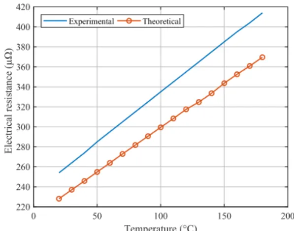
Equation 1 obviously assumes that the heat flow passes only through the interconnection which is not strictly the case. Indeed, some of the leakage heat flux around the interconnection zone will lead to underestimate the thermal resistance of the interconnection, due to natural heat spreading. The kelvin track of the PCBs can be used to measure precisely the ΔT after a calibration sequence. The relation between temperature and resistance is shown in Equation 2 and is very linear for copper in the temperature range of interest.
𝑅 = 𝑅0. (1 + 𝛼. [T − 𝑇0]) = 𝑅0. (1 + 𝛼. ΔT)
Equation 2: Linear model of electrical resistance in function of the temperature
For the track dimensions in our assembly, the theoretical curve is plotted in Figure 9 between 20°C to 180°C with copper temperature coefficient of 𝛼 = 3.9 × 10⁻³ K-1.
The experimental measurement is achieved by
measuring the track electrical resistance (RTOP or
RBOT in Figure 8) at controlled temperature by putting
the PCB in the oven. The measure is taken every 10°C in the same range of the theoretical curve.
Figure 9: Theoretical and experimental curves of the track’s electrical resistance in function of the temperature
The difference between the theoretical and calibration curves can be explained by uncertainty in dimensions (mostly thickness) due to the chemical etching and/or properties of the copper. However, these results show that this method is suitable for a ΔT definition.
Currently, we are considering two complementary routes for measuring the thermal impedance. Firstly, the preparation of a representative sample of the interconnection thermal environment but realized without interconnection to evaluate the thermal resistance of the environment,
On the other hand, a COMSOL Multiphysics® model is in progress to characterize the power dissipated by the interconnection environment and thus to indicate the power passing through the macro-nano structured interface.
Moreover, the assembly can be modified to evacuate the heat from the top side in order to maintain the temperature and to have an accurate value of ΔT. Some experiments demonstrate the feasibility of non-destructive modification of the upper PCB to get a direct access to the inner copper. It makes it possible to implement a cooling system in order to dissipate the heat and therefore to control accurately the ΔT during experiment.
5 Conclusion and Perspectives
The proposed approach of power device packaging is a combination of PCB-embedding technology and full copper macro-nano interconnection. The manufacturing process has the advantage to be carried out only by adding a nano porous membrane in the common electronics product line. The electrical characterization results show a low interconnection resistance, encouraging for a power electronics
integration, while the interconnection is made of full copper favoring heat dissipation of the power switches. The thermal characterization is in progress. In perspective, we expect that this flex interconnection could limit mechanic strains transfer at the interface; this aspect will be treated in a future work.
6 Acknowledgement
The authors thank the SCEL from University of Paul Sabatier, Toulouse 3 for giving their assistance and the access to the lab scale PCB production line equipment.
References
[1] C. Buttay et al., "Application of the PCB-Embedding Technology in Power Electronics – State of the Art and Proposed Development," 2018 Second International Symposium on 3D Power Electronics Integration and Manufacturing (3D-PEIM), College Park, MD, 2018, pp. 1-10.
[2] Kolar Johann W, Krismer Florian and Nee Hans-Peter, “What are the "Big CHALLENGES" in Power Electronics?", 8th International Conference on Integrated Power Electronics Systems (CIPS 2014), Nuremberg, Germany, February 25-27, 2014.
[3] J. W. Kolar and et al., “Approaches to overcome the Google/IEEE Little Box Challenges,” ETH Zurich, Tech. Rep., 2015.
[4] Shur, Michael. (2019). Wide Band Gap Semiconductor Technology: State-of-the-Art. Solid-State Electronics. 10.1016/j.sse.2019.03.020.
[5] M. Meisser, M. Schmenger and T. Blank, "Parasitics in Power Electronic Modules: How parasitic inductance influences switching and how it can be minimized," Proceedings of PCIM Europe 2015; International Exhibition and Conference for Power Electronics, Intelligent Motion, Renewable Energy and Energy Management, Nuremberg, Germany, 2015, pp. 1-8.
[6] G. Regnat, P. Jeannin, D. Frey, J. Ewanchuk, S. V. Mollov and J. Ferrieux, "Optimized Power Modules for Silicon Carbide mosfet," in IEEE Transactions on Industry Applications, vol. 54, no. 2, pp. 1634-1644, March-April 2018. [7] R. Soares, J. Haque and E. Prado, "High-Density
PWB Microvia Reliability for Space Application," 2007 IEEE Aerospace Conference, Big Sky, MT, 2007, pp. 1-8.
[8] L. Ménager, M. Soueidan, B. Allard, V. Bley and B. Schlegel, "A Lab-Scale Alternative Interconnection Solution of Semiconductor Dice Compatible with Power Modules 3-D Integration," in IEEE Transactions on Power Electronics, vol. 25, no. 7, pp. 1667-1670, July 2010.
[9] B. Mouawad et al., "Direct Copper Bonding for Power Interconnects: Design, Manufacturing, and Test," in IEEE Transactions on Components, Packaging and Manufacturing Technology, vol. 5, no. 1, pp. 143-150, Jan. 2015.
[10] Q. H. Luan, V. Bley, T. Lebey, B. Schlegel and L. Menager, "Nano copper wires interconnection for three — dimensional integration in power electronics," 2008 IEEE Power Electronics Specialists Conference, Rhodes, 2008, pp. 278-281.
[11] V. Nguyen et al., "Fabrication of bottom die substrate solderless interconnection based on nano copper wires," 2009 13th European Conference on Power Electronics and Applications, Barcelona, 2009, pp. 1-9.
[12] J. Vobecký, D. Kolesnikov, Reliability of Contacts for Press-Pack High-Power Devices, Microelectronics Reliability, Volume 45, Issues 9–11, 2005, Pages 1676-1681.
[13] F. Lang, U. Scheuermann, Reliability of spring pressure contacts under environmental stress, Microelectronics Reliability, Barcelona, 2009, pp. 1-9.
[14] M.S. Chandrasekar, Malathy Pushpavanam, Pulse and pulse reverse plating — Conceptual, advantages and applications, Electrochimica Acta, Volume 53, Issue 8, 2008, Pages 3313-3322.