Design and Fabrication of Polycrystalline Material Thin-Film Transistors for Active Matrix Liquid-Crystal Display and Static Random
Access Memory Applications
by
Andrew John Tang
B.S., Electrical and Computer Engineering University of Texas at Austin, 1992
Submitted to the Department of Electrical Engineering and Computer Science in partial fulfillment of the requirements for the degree of
Master of Science
in Electrical Engineering and Computer Science at the
Massachusetts Institute of Technology June 1995
© 1995 Massachusetts Institute of Technology. All rights reserved. Signature of
A ub hlo r... ... ... ...
Department of Electrical Engineering and mputer Science May 12, 1995 Certified
... ... ... ... ... ... Ratael Reif Director, Microsystems Technology Laboratories Professor, Department of Electrical Engineering and Computer Science (>,xThesis Supervisor Accepted
b.. ... .. .... ... ... 9Ag-r.r.... .... -. .
'rAA-'SAC:UER' .IN lui'q§,,u, t
OF TECHNOLOGY
. or gnthaler
aredeChairman, Commi ee on Gradu tetudents
Design and Fabrication of Polycrystalline Material Thin-Film Transistors for Active Matrix Liquid-Crystal Display and Static Random
Access Memory Applications
by
Andrew J. Tang
Submitted to the Department of Electrical Engineering and Computer Science on May 12, 1995 in partial fulfillment of the
requirements for the degree of
Master of Science
in Electrical Engineering and Computer Science
ABSTRACT
Polycrystalline silicon germanium ( poly-Si -xGex ) thin-film transistors have been designed and fabricated for applications in the areas of active matrix liquid-crystal display (AMLCD) and static random access memory (SRAM). This project has been completed in four phases: design, fabrication, testing, and device/process modification.
First, the design phase includes device design, unit process development, and process integration. A top-gate TFT is chosen for process and testing simplicity. Unit process development includes active layer film deposition, grain size enhancement, gate dielectric considerations, and gate/source/drain doping and activation. The film deposition
investigation is composed of plasma-enhanced low-pressure chemical vapor deposition (PELPCVD) and low-pressure chemical vapor deposition (LPCVD) of polycrystalline and amorphous films. Further, electrical characterization is done on poly-Sil-xGex using Hall-Effect test structures, and results show higher mobility and lower sheet resistance were possible when the Ge content is optimized. Grain size enhancement techniques explored include amorphous deposition followed by solid-phase crystallization (SPC), polycrystalline deposition, and poly deposition followed by Si implant amorphization and
SPC. Gate dielectric considerations include thermal oxide and low-temperature oxide (LTO). LTO annealing duration and gate/source/drain dopant activation are also optimized. Second, the fabrication involves a low-temperature(< 625°C) 0.8 gtm self-aligned
NMOS/PMOS Si process with four levels of device-definition masks plus two implant split masks. Device separation was done by mesa island isolation of the active layer. Fabricated device sizes range from 0.5 gtm to 60 gtm drawn gate length and width.
Third, device testing includes typical IDS vs. VDS transfer curves, IDS vs. VGS transfer characteristics, and activation energy determination. Mobility, threshold voltage,
subthreshold slope, and leakage current are measured using IDS vs. VGS curves. Further, temperature-dependent IDS vs. VGS curves are used to measure the activation energy. Finally, a poly-Si-capped poly-Sil .xGex TFr structure is designed to improve the gate oxide interfacial quality of poly-Si 1-xGex TFTs. Fabrication of poly-Si-capped poly-Si 1 xGex TFTs requires only a 10% modification of the conventional process.
The major contribution of this project to the polycrystalline material TFIT research can be summarized by the results of high-temperature (< 1000°C) processed and
low-temperature (< 625°C) processed TFTs. High-low-temperature processed poly-Si-capped poly-Sio.9Geo. 1 TFTs with thermal oxide were found to have the highest mobility reported-to-date, for poly-Sil IxGex, of 51 cm2/V-sec for p-channel devices and 41 cm2/V-sec for n-channel devices. This is compared to the hole mobility of 27 cm2/V-sec and the electron mobility of 45 cm2/V-sec for similarly processed poly-Si TFTs. Low-temperature processed poly-Sio.88Geo.12 TFTs were also measured to have the highest mobility reported-to-date, for poly-Sil xGex, of 35 cm2/V-sec for hole and 28 cm2/V-sec for electrons. This is compared to the hole mobility of 26 cm2/V-sec and the electron mobility of 29 cm2/V-sec for similarly processed poly-Si TFTs.
Thesis Supervisor: Rafael Reif
Title: Director, Microsystems Technology Laboratories
Acknowledgments: The single most read page in a thesis
°I thank my parents for everything they have done for me to get me this far. They have sacrificed much of what they had yesterday to make me much of what I am today. The most thanks go to Professor Reif. If I were given a chance to go back in time and choose my advisor all over again, I would have chosen to work for him in a heartbeat. Thank you for your guidance, advice, support, tolerance, patience, and countless other little things that made my graduate work most rewarding and memorable. Special thanks also go to Carolyn Zaccaria for keeping our group as well as the whole MTL under control! The "most most" thanks go to the senior graduate student, Dr. Julie A. Tsai, who has been a knowledgeable consultant, neat officemate, really good friend, and a small big sister Thanks for laying down the strong foundation for our project which made my master's work a breeze. Special thanks also go to Dr. Tsu-Jae King at the Xerox PARC who has helped me finished my experimental work ( hydrogenation ) as well as making me understand what it takes to become successful in this business. Thanks also go to Dr. T. Noguchi for helping me design my experiments.
Thanks also go to Dr. Julie A. Tsai and Batman ( Ben A. Tao ) for making our office the happening place in the building, the only office in MTL that has a TV, fridge, speakers, CD player, cordless phone, tons of CDs, a cat, truck load of junk food: my bubble gums, Julie's gummy bears, Ben's Slim Jims ... Many thanks also go to Reif group members for special friendships that will last a life time, and especially: Ben Tao for financial
support, Dr. Julie Tsai for not making me do TEMs, Ken Liao for his technical consulting, Rajan Naik for redefining the meaning of a gentleman, Weize Chen for UNIX help and the occasional Chinese refresher courses, Simon Karecki for friendship, and Dr. Zhen Zhou for friendship.
Thanks also go to Dr. "Nori" Yamauchi and Dr. Jim Pfiester for helping me design my experiments. Lots of thanks for technical assistance also go to Jeff Kim, Daniel Maung, Dr. Jarvis Jacobs, Lalitha Parameswaran, Bo Zheng, Joe Lutsky, Dr. Curt Tsai ( root beer consultant ),Professor Jesus del Alamo for technical consulting and excellent teaching, Jee-Hoon Yap, Wenjie Jiang, Andy Wei, Paul Yu, Dennis Ouma, and Melanie Sherony. Thanks also go to Professor Kayvan Sadra, Professor Ben Streetman, and Professor Sanjay Banerjee for introducing me to the exciting research of semiconductor processing! And of course, I am indebted to the awesome ICL/TRL staff for taking care of my wafers! You guys are the best!!! Also, lots of thanks go to Sam Crooks for thesis preparation. I would also like to thank my friends outside of MTL: Andy Tsai for teaching me how to be more forgiving, Daniel Maung for showing me how to be smooth, Donald Tanguay for convincing me to be adventurous, confident, and aggressive, and Kate Nguyen for
showing me how to be humble. Oh! and Jeff Kim for deep thoughts! Finally, thanks go to Patrick Yue, Dawn Farber, Tuong Le, Matt Sinn, Amy Duwel, Jeff Thomas, cuzzies Wei-Ling and Amy, and brother Eric for simply being there for me when I needed them.
Contents
Abstract 2 Acknowledgments 4 List of Figures 7 List of Tables 9 1 Introduction 10 1.1 Applications of TFTs 111.2 Motivation for using poly-Si.~Ge. TFTs 14
2 A Brief Review of Semiconductor Device Physics 15
2.1 Metal-Oxide-Semiconductor (MOS) 16
2.2 Metal-Oxide-Semiconductor Field-Effect Transistors (MOSFET) 17
2.3 Thin-Film Transistor (TFT) 20
2.4 Hall effect 22
3 Process and Device Design of Polycrystalline Material TFTs 24
3.1 Active layer design 25
3.1.1 Trade-offs between Si and Si Ge. films 25 3.1.2 Trade-offs between poly and amorphous films 28
3.2 Grain enhancement techniques 29
3.2.1 Amorphization 29
3.2.2 (Re)crystallization 32
3.3 Gate dielectric considerations 33
4 Measured Current-Voltage Transfer Characteristics for
Poly-Si0.88Ge0 1 2 TFTs
4.1 Fabrication process 4.2 Results and discussion
5 Poly-Si-Capped Poly-Sil..Ge, TFTs
5.1 Motivation
5.2 Experimental design and fabrication 5.3 Measured TFT characteristics
6 Conclusions and Future Work
Appendices A. B. C. D. Bibliography
Process traveler for LTO capacitor experiment Process traveler for Hall-effect experiment Process traveler for TFT2 experiment Process traveler for TFT3 experiment
37 38 39 47 48 49 51 58 61 62 64 70 75 81
List of Figures
Figure 1.1 A typical TFT structure. 11
Figure 1.2 A typical SWL SRAM cell with TFT pull-up transistors. a) Two single crystalline access transistors and two pull-down transistors. b) Two
TFT pull-up transistors. 13
Figure 2.1 A typical self-aligned n-channel MOSFET. 17
Figure 2.2 Seto's grain boundary model. 20
Figure 2.3 Depiction of Hall effect. 22
Figure 3.1 Hall-effect test structure. 26
Figure 3.2a Resistivity as a function of Ge content. 27
Figure 3.2b Hall mobility as a function of Ge content. 27 Figure 3.3 Grain size as a function of Ge content and active layer formation
methods. 31
Figure 3.4 A LTO capacitor test structure. 34
Figure 3.5 Rs of S/D area of TFTs as a function of Ge content. 36
Figure 4.1. Structure of a top-gate TFT. 39
Figure 4.2. Typical IDs vs. VGs transfer characteristics for devices with W=L=5 Am
at IVDsl=10 V. (a) n-channel; (b) p-channel. 40
Figure 4.3a Eaas a function of VGS at IVDSI=O. 1 V for devices with W=L=5 gm. 44
Figure 4.3b Arrhenius plot of IDS vs. 1/KT with IVDSI=O0.1 V and n-channel poly-Si TFT W=L=5 gm at various VGS for the determination of Ea. 44 Figure 4.3c Arrhenius plot of IDS vs. 1/KT with IVDSI=0.1V and p-channel poly-Si
TFT W=L=5 pum at various VGS for the determination of Ea. 45 Figure 4.3d Arrhenius plot of IDS vs. 1/KT with IVDSI=O0.1 V and n-channel
poly-Si0.88Ge0.12 TFT W=L=5 gm at various VGS for the determination of Ea. 45
Figure 4.3e Arrhenius plot of IDS vs. 1/KT with IVDSI=O. 1V and n-channel poly-Si0.gsGeo.12 TFT W=L=5 pum at various VGs for the determination of
Ea. 46
Figure 5.2a
Figure 5.2b
Pre-hydrogenation I-V characteristics for n-channel poly-Si-capped poly-Sil xGex TFTs with thermal oxide.
Pre-hydrogenation I-V characteristics for p-channel poly-Si-capped poly-Sil xGe. TFTs with thermal oxide.
56
List of Tables
Table 3.1 Trade-offs between different types of films. 29
Table 3.2 Poly to amorphous transition temperatures. 30
Table 3.3 Si implant optimization. 30
Table 3.4 Various (re)crystallization techniques. 33
Table 3.5 Results of the LTO capacitor experiment. 35
Table 4.1. Electrical characteristics for poly-Sil-xGex and poly-Si TFTs with W=L=Sgm and IVDSI=10 V. (a) before hydrogenation; (b) after
hydrogenation. 42
Table 5.1 Experimental split chart of TFT3. 51
Table 5.2 Measured TFT performance before hydrogenation for L=W=0.5 gtm
devices. 52
Table 5.3 Measured TFT performance before hydrogenation for L=W=0.75 gim
devices. 54
Table 5.4a Measured poly-Si-capped poly-SiogGe0o. TFT with thermal oxide performance after 4 hours of hydrogenation for L=W=3 gm n-channel
devices. 55
Table 5.4b Measured poly-Si-capped poly-Si0o.gGe0o. TFT with thermal oxide
performance after 4 hours of hydrogenation for L=W=3 gm p-channel
Chapter 1
Thin-film transistors (TFTs) [1] (Figure 1.1) belong to a novel class of transistors that have a similar structure to metal-oxide-semiconductor field-effect transistors (MOSFETs), devices that are the basic building blocks of virtually all integrated circuits. Although the conventional MOSFET technology is far more mature and advanced than the TFT technology, there are many applications where it is impossible to use the conventional MOSFET technology. These applications usually involve transistors being constructed on an amorphous substrate such as glass or silicon dioxide. These areas first became the niche for TFTs, then they emerge as markets of its own class. Some of the most important TFT applications include liquid crystal displays (LCDs) [2-3], static random access
memories (SRAMs)[4,5], and image sensors [6,7].
Undoped polycrystalline channel layer
Fig. 1.1: A typical TFT structure.
1.1 Applications of TFTs:
LCDs
LCD is a type of display that relies pixel control on liquid crystals, voltage-controlled light filters. The most important part of building a LCD is the formation of the voltage
controllers which are usually made by transistor switches. Since LCDs require transparent substrates to house both the transistor switches and the liquid crystals, an ideal choice for the substrate is glass. Because glass is amorphous, conventional MOSFET technology is not applicable; therefore, TFTs are the ideal candidates for such applications.
Another part of an LCD is the peripheral circuit element. Peripheral circuit elements of an LCD usually include shift registers, drivers, and combinational logic circuits. These peripheral elements are usually done by employing application specific integrated circuits (ASICs) using conventional MOSFET technology[3]. However, it will be far more economical to build ASICs on the same glass substrate along with the transistor switches [2,3]; furthermore, with a totally integrated system, signals from the peripheral circuits are better transmitted and received since they are not required to go off-chip.
Amorphous Si was first used in the TFT technology for its process simplicity and low leakage current[2], and are suitable for the transistor switches. However, because of its lower mobility, amorphous Si TFTIs do not qualify to be used as the peripheral circuit elements. Therefore, the latest trend calls for a high-mobility material, polycrystalline Si ( poly-Si ) [2], to serve as pixel controllers as well as the peripheral circuit elements[3].
SRAMs
An SRAM cell consists of two access transistors controlled by the word line[5] and a flip flop which is made up of two Complimentary Metal Oxide Semiconductor (CMOS) inverters. Furthermore, a CMOS inverter consists a pull-up and a pull-down transistor. Finally, a pull-down transistor is defined as a transistor that provides a current sink to the electrical ground when the transistor is turned on; on the other hand, a pull-up transistor is a transistor which provides a current path to the power supply (Vdd) when the transistor is turned on.
The earliest CMOS SRAM cell is called the 6-T cell which consists of six conventional MOSFETs; later, the 6-T cell evolved into the 4-T+2-R cell with four MOSFETs plus two
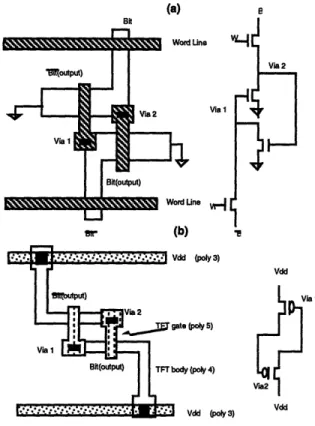
polycrystalline resistors serving as the pull-up devices; as of today, the SRAM cell has matured to an elegant split-word-line (SWL) SRAM cell (Fig. 2) which employs four MOSFETs plus two pull-up TFTs[4,5]. The SWL TFT SRAM cell has the advantage of compactness over the 6-T cell and the advantage of higher on/off current ratio over the 4-T+2R design[5]. (a) e Bt I Via 2 Vial1 or (b) 1 3) Vdd Via 1 vm2 Po 3) Vdd
Fig. 1.2: A typical SWL SRAM cell with TFT pull-up transistors. a) Two single crystalline access transistors and two pull-down transistors. b) Two TFT pull-up transistors [6].
Image Sensors
Contact-type linear image sensors are commonly used in facsimiles and optical scanners because of their compactness and the cost-advantage due to the minimum requirements for optical components [6,7]. Each pixel of these sensors consists of a detector based on amorphous Si TFT and an analog switch. Signal is read out from each pixel by turning on its switch and transferring the charge stored in the detector to an external amplifier. Similar
to the development of LCDs, it is very important to integrate the amorphous Si sensors, the analog switch, and the external amplifier. Consequently, a material with higher mobility is required to ensure enough circuit speed and current drive for such an integration[O10].
1.2 Motivation for using polycrystalline silicon germanium alloy thin film
transistors
Current drive of TFTs is directly proportional to the average grain size of the TFT channel layer. As a result, numerous grain-size enhancement techniques were proposed, and the two major techniques are solid phase crystallization (SPC) [8-13] and Excimer laser
annealing (ELA) [14].
T.-J. King et. al. have approached this problem by using poly-Si.xGexas a replacement for
poly-Si in the active layer of the TFT structure without changing any other process parameters[15-17]. Poly-Sil.xGexoffers higher mobility and lower processing
temperatures than poly-Si[18-20]. Higher mobilities provide higher circuit speed, and lower processing temperatures allow the flexibility of using cheaper substrates. The design
and fabrication of poly-Si,.xGexTFTs are covered in Chapter 3. But first, the fundamental
device physics are reviewed in Chapter 2 because they are the prerequisites for the device and process design in Chapter 3.
Chapter
2
A Brief Review of Semiconductor Device
Physics
2.1 Metal-Oxide-Semiconductor (MOS)
An ideal MOS capacitor can be characterized by several device parameters: threshold voltage (Vth), interface trap density ( Qi ), breakdown voltage(VBr), and leakage current (IL) [21]. Vth can be well controlled by doping levels and device dimensions; on the other hand, V}, Qi, and IL are mainly controlled by the choice of gate dielectric as well as the history of the thermal treatment. Some of the most important governing equations for MOS capacitors are listed below:
Flat band voltage = VFB = iVms - (2.1.1)Qi
COox
Threshold volatage = Vth = VFB - d + 2 f (2.1.2)
Cox
Vms = Vm- Vs (2.1.3)
Qi = interface traps density (2.1.4)
Cox E°x (2.1.5)
tox
Qd =2 AqsNAn1f
(2.1.6)
KT n N A
q ni f q nil ~~~~~~~~~~~~~(2.1.7)
Since LTO is commonly used as the gate dielectric of a low-temperature processed TFT, VB and IL are the two figures of merit we monitor. Optimization of the gate dielectric and dielectric densification will be covered in Section 3.3.
2.2 Metal-Oxide-Semiconductor Field-Effect Transistor (MOSFET)
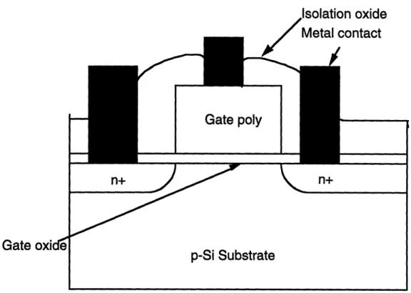
MOSFET is a three-terminal voltage-controlled current source [21], as seen in figure 2.1. The gate voltage (VGs) serves as the switch to the current source between the source and drain terminals. Similar to the MOS structure, the switch is turned on after the gate voltage exceeds the threshold voltage.
Isolation oxide
Metal contact
L'
Gate
Figure 2.1 A typical self-aligned n-channel MOSFET
There are three distinctive regions in the operation of a MOSFET: cutoff, linear, and saturation. First, the cutoff region is defined as the off state of the device when VGS < Vth. Next, the linear region is defined as the region where VGS > Vth and also
VGD>Vth. Finally, the saturation is defined as the region where VDS is high enough that
-VGD is no longer effective enough to invert the entire channel, or the occurrence of pinch-off at the drain end. This region is characterized by VGS>Vth and VGD<Vth.
Some figures of merit of MOSFET are Vth, field-effect mobility, subthreshold slope, and leakage current. Some of the governing equations in MOSFETs are derived in this section [21]. (2.2.1) through (2.2.10) are shown on the next page with CG being the gate
capacitance, QE being the inversion charge density, E being the electric field in the channel, T being the channel transit time, VDSsat being the effective VDS in the saturation regime, and SS being the subthreshold slope. (2.2.1) through (2.2.5) are from the fundamental physics of solid, and (2.2.6) was obtained by the substitution of VGS with (VGS-VDS/2
) into (2.2.5). In the linear region, the voltage at the center of the channel can be approximated as VDs/2; thus the effective gate voltage is VGs-VDS/2 instead of just VGs, as used in (2.2.5). In the saturation regime, IDS reaches a saturated value when VDS is increase to VDsSat. At that point, IDS is determined by drift velocity of carriers across the pinch-off depletion region at the drain end. In this region VDS is replaced by the effective VDS, or VDsat. Results are shown in (2.2.7). Finally, subthreshold swing, which defines how sharp transistors turn on, is shown in (2.2.10) and (2.2.11).
Derivation of IDS: CG = WL tox QE = (VGS - Vth) ' CG E= VDS L L Ve-= Vel L = gE 11VDSLVDs IDS -QE _ (VG - Vth)-CG Liner- L2 9VDS Linear Regime: IDS = eoxWt[(VGs toxL -Vth) VDS (VDS)2 ] 2 Saturation Regime: £OXWI1 ~~(VDS~at)
IDS= Wt [(VGS -Vth) VDSsat (VDSsat)22 1
VDSSat = VGS-V th
IDS = EOWL[(VGS - Vth)2]
IDS= I ,,
-toxL L
Definition of Subthreshold Slope:
SS = n(10)
dVG(nDs)
Zd(IDS )
SS- q nlO.(+ Cd
) q Cox (2.2.1) (2.2.2) (2.2.3) (2.2.4) (2.2.5) (2.2.6) (2.2.7) (2.2.8) (2.2.9) (2.2.10) (2.2.11).
II i
lS
Eb
X
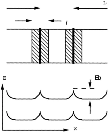
Figure 2.2 Seto's grain boundary model
2.3 Thin-Film Transistor (TFT)
TFTs can be considered as a special type of silicon on insulator (SOI) with the exception of the active layer of the transistor, which is made of polycrystalline material. The ideal current equations [21] derived for MOSFET will be modified according to Seto's grain boundary carrier hopping theory[22]. Seto proposed to model polycrystalline films as a collection of single crystalline regions (see figure 2.2) separated by sheet charge of grain boundary traps, NT. The grain boundary traps also create a depletion region which serves as a potential hill to carriers. The equations that describe this theory are summarized in (2.4.1) and (2.4.2). Vb is defined as the grain boundary height carriers must surmount in
E
order to participate in conduction. Modified device parameters and current equations with the effects of NT are shown in (2.4.3) through (2.4.6).
Bulk properties: 2 Vb= 8 qN 8eoESNA (2.4.1) and -eVb
2.km
2k
=
2;r kT me**e
TFT device parameters and current-voltage relations:
Vth = VFB- Qd + 2 f + NT
Cox Cox
IDS = o Ci (W / L) .(VGS
- Vth)
.VDS .
e
(E a /KT)
yFE = guo e(Ea / KT)
SS kTln1O.( C + q d NT) q Cox Cox (2.4.2) (2.4.3) (2.4.4) (2.4.5) (2.4.6)
where Cd is the depletion capacitance, Cox is the gate capacitance, m* is the carrier effective mass, NA is the dopant concentration, and Ea is the activation energy for field-effect mobility.
2.4 The Hall effect
If a magnetic field is applied perpendicular to the direction in which holes drift in a p-type semiconductor, the path of the holes tends to be deflected (Fig. 2.3). This phenomenon is known as the Hall effect [21].
Known parameters: Bz,Ix Measured parameters: Vy=VAB,V=VCD Calculated parameters p, rho, and mu
Figure 2.3 Depiction of Hall effect
The total force exerted on the hole is shown in (2.5.1):
Fy =q(Ey-v xB)
Ey = vxBz (2.5.1)
Since we know that the holes are not accelerating in the y-direction, Fy must be balanced or zero. This calls for a built-in electric field, Ey, that counterbalances the force generated by
the cross product of the magnetic field and the velocity in the x-direction. Also, the saturation velocity, v, can be expressed in terms of charge, concentration, and current density. This is summarized in (2.5.2) below:
Ey
=-
JxBz =
RHJxBz (2.5.2)qPo
Further, we can solve for the active carrier concentration by rearranging (2.5.2). Carrier concentration is then shown in (2.5.3):
PO=
Jx BZ= Ix ' Bz (2.5.3)-
qE~~~~~
qtV~~~~~~~
(2.5.3)
qEy qtVAB
Resistivity can be solved without using the external magnetic field; however, Hall mobility determination requires both the resistivity and the Hall coefficient which is obtained under a external magnetic field. Resulting equations are shown below:
Rwt VCD/IX (2.5.4)
L Llwt
a = RH (2.5.6)
Chapter 3
Process and Device Design of
Polycrystalline Material TFTs
TFTs are usually fabricated on an amorphous medium which can be either glass or
interlevel dielectric. The TFT process begins with the active layer film deposition and grain enhancement. Then, gate dielectric and gate electrode definition take place, followed by source/drain/gate dopant implantation and activation. Next, isolation oxide is deposited and contact cuts are made. Finally, Al is sputtered and patterned to serve as electrical contacts and plasma hydrogenation is performed.
3.1 Active layer design
We are interested in two main types of materials: silicon and silicon germanium. In addition, we have looked at the different options of deposition technology: low pressure chemical vapor deposition (LPCVD) and plasma-enhanced LPCVD ( PELPCVD ). Finally, we have also explored the option of amorphous Si and Sil-xGex deposition.
3.1.1 Trade-offs between the use of Sil-xGex and Sifilms by Hall-Effect test structures
To find out the trade-offs between Si -xGex and Si films, electrical characterization of resistivity and mobility as a function of Ge content is obtained using Hall-effect test structures shown in figure 3.1 [18,19] (See Appendix B). Si substrate is used as the starting material, then a 5000A of thermal oxide is grown. Next, about 1000A of poly-Sil -xGex is deposited on the samples. One light blanket implant is used as the doping of the film while a heavy contact implant is done in the contact area to form ohmic contacts. For electrical isolation, 3000A of LTO is deposited, then contact holes are formed and
A1-1%Si is sputter-deposited and patterned. Finally, sintering in H2/N2is done before the Hall measurements.
zc7
Figure 3.1 Hall-effect test structure
The results of the Hall-effect experiment are shown below in Fig. 3.2a and Fig. 3.2b. From the figures, hole mobility increases with the increase in Ge content until a critical Ge content is reached; on the other hand, electron mobility increases monotonically for all the Ge content attempted in this experiment. Finally, the resistivity seemed to be lowered as more Ge is alloyed with poly-Si, and the trend seems to continue for Ge content of up to 32%.
10lT 10' 10l
Dopant Concentration (cm4)
Figure 3.2a Resistivity as a function of Ge content
50 U I 40 E u s0 .0 a 20 10 0 0o 1 10 20 GB content (atomic %) F
Figure 3.2b Hall mobility as a function of Ge content.
104 10o' 10' U 'A n 10' 1 0 t lo 2 2 40% Ge O[-20% Ge A--A32% Ge ... . . . -10. *-- *n-type -Op-type I! 30 40 ... i...·... lo' iu _ _ 10 z ° I I I
-3.1.2 Trade-offs between the use of Poly and amorphous films
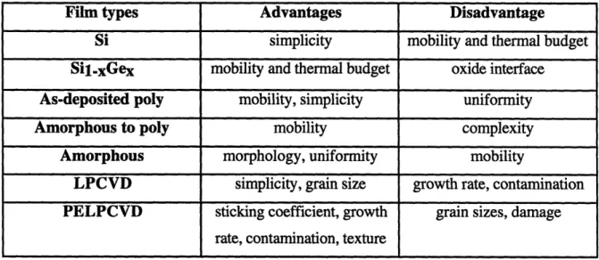
With regard to the choice between polycrystalline and amorphous materials, polycrystalline materials provide higher mobility while the amorphous materials provide lower leakage, better surface morphology, better uniformity, and lower thermal budget. Nevertheless, polycrystalline films can be formed from amorphous films, and they generally have higher mobility, larger grains, and lower leakage currents than the as-deposited polycrystalline films. The two major deposition systems, LPCVD and PELPCVD, are also compared for the applications of poly-Si and poly-Si 1 -xGex. Since GeO is volatile, PELPCVD is preferred for the poly-Sil -xGex deposition for its higher Ge sticking coefficient on oxide; further, PELPCVD provides higher deposition rate and thereby increases throughput. PELPCVD also offers stronger textured grains which reduces misalignment angle between grains. Although PELPCVD provides many attractive features to the film deposition, LPCVD films are still widely used due to its simplicity and availability.
The different types of films available are summarized in Table 3.1 with the pros and cons associated with each method.
Table 3.1 Trade-offs between different types of films
Film types Advantages Disadvantage
Si simplicity mobility and thermal budget
Sil-xGex mobility and thermal budget oxide interface
As-deposited poly mobility, simplicity uniformity
Amorphous to poly mobility complexity
Amorphous morphology, uniformity mobility
LPCVD simplicity, grain size growth rate, contamination
PELPCVD sticking coefficient, growth grain sizes, damage
3.2 Grain enhancement techniques
Equation (2.4.2) is rewritten below, and it governs the transport mechanism in poly films. It is easy to see that the mobility is linearly related to the grain size L. Therefore, it is very important that the grain size be maximized using various type of amorphization and subsequent annealing techniques.
-eVb
= q*L *-e kT. (3.2.1)
2r. kT me
3.2.1 Amorphization
The amorphization techniques that will be discussed here consist of amorphous deposition and polycrystalline deposition with Si implant [8-10]. Amorphous deposition is
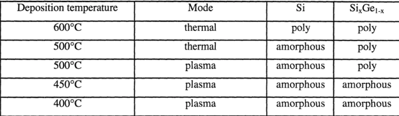
accomplished by simply carrying out the normal deposition at a temperature lower than the polycrystalline/amorphous transition temperature (Table 3.2) [18]; however, the growth rate may be very low at such temperatures and plasma deposition is required to enhance the deposition rate. Another amorphization technique is the option of polycrystalline
deposition with subsequent Si implantation [10]. This technique is more costly than the former and also more complicated; however, Si implantation provides a more thorough amorphization and therefore yields larger grains (figure 3.3). We have also found the optimized dose of Si for amorphization, and the results are summarized in Table 3.3.
Deposition temperature Mode Si Si.Gel-.
600°C thermal poly poly
500°C thermal amorphous poly
500°C plasma amorphous poly
450°C plasma amorphous amorphous
4000C plasma amorphous amorphous
Table 3.2 Poly to amorphous transition temperatures
Ge content/Si implant dose lel4 cm2 5el4 cm 2 1e15 cm 2
,~~ e ~~~ 14 ~ 2 514c cm'1e15m-
-0% poly poly amorph
10% poly NA amorph
25% poly amorph amorph
43% poly amorph amorph
Is1'
El--10 20 30
Go content (atom ic %)
40
}- - OaQ'c Thermal Poly (aaA)
'I---[a5 C ThoMral Poly (A)
*---EIac'C Pkama Poly (1SaaA)
- --- V4aaO'C Pkama Am orph, afc crystmizod (saCA)
#---poly, Amorphizod, saacC racallizod {IaaaA)
Figure 3.3 Grain size as a function of Ge content and active layer formation method.
1.00 I aa= . ,CL 0.10 I 4 I 0 0.01 B . B . x . E - I*
---
---- V
I- - [D;. Z 03.2.2 (Re)crystallization
After an amorphous film is obtained, several annealing techniques have been proposed and used to recrystallize the amorphous film. First, solid phase crystallization (SPC) provides the traditional furnace annealing which lasts from 20 hours to 60 hours usually at low temperatures (-600°C) [8,10-13]. SPC suffers from the low throughput and ineffective annealing of intragranular defects; however, SPC is capable of producing the largest grains among all other techniques because of its slower process. Excimer laser annealing ( ELA) has become more attractive recently because of the improving stability of lasers. In
general, ELA-processed samples produces films with smaller but uniform grains; more importantly, ELA-processed TFTs are usually the highest performance devices [14]. Finally, we have briefly examined rapid thermal annealed TFTs which yield reasonably good performance, but its effect on the underlying glass substrate is still to be investigated. Table 3.4 summarizes the different (re)crystallization techniques.
Table 3.4 Various (re)crystallization techniques
3.3 Gate dielectric considerations
The process parameters regarding gate dielectric annealing and dopant activation are optimized in a single experiment using LTO capacitors. P-type Si substrates are used and
oo1000A
of LTO is deposited. Next, samples are annealed in nitrogen at 600°C for either 0,12,24, or 36 hours before 3500A of poly-Si is deposited at 625°C. Then, either a single implant or a double implant scheme is used to dope the poly-Si top plate of the LTO capacitor. The single implant is designed to have a dose of 2e15/cm2B at 30 KeV; on theother hand, the double implant composes of an le15 B/cm2blanket implant at 65 KeV and
a 2e15 B/cm2implant at 30 KeV. Dopant activation is carried out in N2at 600°C for either 0.5 or 2 hours. Fowler-Nordheim measurements are done, and voltage operation range was defined as the gate voltage range for which leakage current is less than 10 nA. Arbitrary resistance measurements are also done by simple V/I evaluation of the heavily
Amorphization Annealing Advantage Disadvantage
Amorphous as SPC Surface Smaller grain
deposited morphology
Si implant SPC Larger grain Process
complexity
Si implant ELA High mobility, Process
higher complexity throughput
Si implant RTA Process Deformation of
simplicity, high glass substrate. mobility
Amorphous as RTA High mobility Smaller grain deposited
doped poly-Si gate. The exact process traveler is in Appendix A. An LTO test structure is shown in Figure 3.4 and results are summarized in Table 3.5.
24-hour LTO densification was chosen according to the measured break-down voltage and leakage current. For the G/S/D doping, a single self-aligned G/S/D B implant was chosen over the double implant because of throughput and process simplicity considerations. Sheet resistance improvement of only 50% is achieved using the more complicated double implant scheme. Further, a 30-minute implant anneal in nitrogen at 600°C was chosen because any additional annealing in the same ambient does not enhance the sheet resistance much further.
p+ poly-Si
Si Substrate
Table 3.5 Results of the LTO experiment: optimized split is high-lighted
Other gate dielectrics have also been explored: thermal oxide and rapid thermal oxide. The results of TFT performance with other dielectrics are covered in Chapter 5.
3.4 Gate electrode, source, and drain doping control and activation
P+ gate electrode is optimized using the LTO experiment. 2e 15 B/cm2is chosen for a self-aligned implant. SUPREM simulation is performed to target the peak of the implant profile at the center of the source, drain, at gate electrode. Since the gate electrode is usually much thicker than the source or drain, compromise is made when choosing the implant
Densification Implant split Dopant Voltage Resistance duration ( hrs) activation( hrs.) operation range (arbitrary units)
(v)
0 double 2 0 12 double 0.5 5 59 12 double 2 50 12 single 0.5 10 59 12 single 2 25 24 double 0.5 50 58 24 double 2 50 58 24 single 0.5 60 110 24 single 2 55 110 36 double 0.5 50 36 double 2 70 55 36 single 0.5 40 100 36 single 2 45 106nitrogen ambient. Sheet resistance of source/drain area of a TFT is measured and shown in figure 3.5. 10, WI 10 R of S/D area of TFTs O3 LPCVD-n O LPCVD-p A PEVD-n a V PECVD-p A 0 v 0 0 10 20 Go oraent 30
Chapter 4
Measured Current-Voltage Transfer
4.1 Fabrication process
We have fabricated poly-SilxGex TFTs with a top-gate structure as shown in Figure 4.1 (See Appendix C). First, 5000K of thermal oxide is grown on bare 4-inch silicon
substrates, then approximately 1000A of poly-SilxGex is deposited and patterned to serve as the active layer of the device. A Si implant with a dose of 2x10¹⁵ /cm2and with the
implant peak at the center of the film is done to amorphize the film; subsequently, a 60-hour solid phase crystallization anneal is performed at 600°C in nitrogen (N2) gas.
Following channel definition, 1000A of low-temperature oxide is deposited as the gate dielectric and 3000A of polycrystalline silicon (poly-Si) is then deposited at 625°C as the gate electrode. Once the gate is defined, the source/drain/gate doping is achieved using a single self-aligned implant with a 2x1015 cm'2dose of boron for p-type doping or
phosphorus for n-type doping. Further, 3000A of low-temperature oxide is deposited as the passivation layer, and dopant activation is performed in N2at 600°C. After the dopant
activation, 1 gtm of A1-1% Si is sputtered and patterned for use as electrical contacts. Finally, devices are sintered at 400°C in a N2/H2mixture. The performance of devices is
evaluated both before and after hydrogenation which is performed in a parallel-plate plasma reactor at 350°C.
'd-1% Si
/Poly SiA- Ar
Si substrate
Figure 4.1. Structure of a top-gate TFT.
4.2 Results and discussion
Typical IDS vs. VGS transfer characteristics for poly-Sil.xGex TFTs before and after hydrogenation are shown in Figure 4.2(a) for n-channel devices and in Figure 4.2(b) for p-channel devices. Device parameters such as effective field-effect mobilities (tmE), threshold voltages (Vth), subthreshold slopes, and leakage currents are derived and
summarized in Table 4.1. gFE is measured at IVDSI= 0.1 V while Vth is defined as the VGs
at which IDS reaches 100 nA with IVDSI = 10 V. Further, with IVDSI= 10 V, the
subthreshold slope is read from the IDS vs. VGS curve while the leakage current is defined as the minimum stable off-state current.
In-
3 ydrogenation ydrogenationi -- I/
< 1 / !9 / i.88 Ge.12 0.88 Ge0.12 / I I 1, II/
I -60 -40 -200
20
40
60
80
Gate to source voltage, VGS (
V )
(a) IV 10 - 4 10-5 10-6 10- 7 10-8 10- 9 1o-1o <Cn c)
0
so0
::0
Cn -r--Ct Qo · ~,, so1-11
... r , i i i BtJ r I I I I I I I I4 ^-3 lU 10.4 10-5
106
10- 7 10-8 10-9 -in-10-80
-60
-80
-60
-40
-20
0
20
40
60
Gate to source voltage,
VGS (
V )
(b)
Typical IDS vs. VGS transfer characteristics for devices with W=L=5 gm at IVDSI=10 V. (a) n-channel; (b) p-channel.
0
CI) to©
¢
Cn0
a)
Lion tion P -4 Figure 4.2. -. 1 __.-I illAt . . ! I BDevice Types n-channel p-channel TFT Channel Material Si Sio0.88Ge0.1 Si SiO.88Geo.12
2
Field-Effect Mobility ( cm2/V-Sec) 21 12 18 22
.~~~~~~~~~~~~~~~~~~~~~~~~~~~~~~~~~~~~~~
Threshold Voltage (V) 15 32 -9 -15
Subthreshold Slope (V/dec) 3.0 4.9 3.3 7.1
Leakage Current (pA) 100 1000 1000 1000
(a)
Device Types n-channel p-channel
TFT Channel Material Si Si0.88Geo.1 Si SiO.88Geo.1 2 2
Field-Effect Mobility ( cm2NV-Sec) 29 28 26 35
Threshold Voltage (V) 4 8 -8 -3
Subthreshold Slope (V/dec) 1.8 1.6 2.9 1.8
Leakage Current (pA) 100 150 100 100
(b)
Table 4.1. Electrical characteristics for poly-Sij.xGex and poly-Si TFTs with W=L=5 gm and IVDsl=10 V. (a) before hydrogenation; (b) after hydrogenation.
From Table 4.1, post-hydrogenation improvement in aFE and Vth shows that the
hydrogenation process is very efficient and essential for defect passivation in the poly-Si0.88GeO.12TFTs. As a result, higher gxE, lower threshold voltage, and steeper
subthreshold swing were achieved after hydrogenation. Also from Table 4.1,
poly-SiO.88GeO.12TFTs have comparable leakage currents as poly-Si devices despite the narrower
bandgap of poly-SijxGex. This is because the leakage current arises from trap-to-band tunneling and thermionic emission [23], rather than band-to-band tunneling.
From Table 4.1, p-channel poly-SiO.8 8Ge0.12 devices have greater values of gm than
n-channel poly-Sio.88Geo.12devices. Although grain boundaries in poly-Si can trap either
electrons or holes, grain boundaries in poly-Sio.88Geo.12 are more efficient at trapping
electrons than holes; this model is consistent with the reported behavior of poly-Ge grain boundaries which trap mainly electrons [24]. To further investigate the hole mobility of poly- SiO.88Ge0O12, we can look at the thermionic emission model. According to this model,
IDS in the linear region, where VDs is small and the quadratic VDS term is disregarded, can be expressed as:
IDS = to ' Ci (W/ L) (VGS - Vth ). VDS e- ( E a /KT) (4.2.1)
and
AlFE =
lo e
(Ea KT) (4.2.2)where Ea is the activation energy, Ciis the gate capacitance, and go is the intragranular carrier mobility [25]. For the determination of Ea, IDS vs. VGS curves were recorded at temperatures 30°C, 50°C, 75°C, and 100°C with IVDSI=0.1 V. (4.2.1) is used to calculated Ea from the slope of the straight-line Arrhenius plot of log IDS versus 1/kT for each VGS. In figure 4.3, Ea is plotted as a function of VGS for both Si and
poly-Sio.88Geo.12. Despite the higher activation energy, gFE of p-channel poly-SiO.88Ge.12devices
is enhanced over that of p-channel poly-Si devices by more than 30%, from Table 4.1. The higher intrinsic mobility values of poly-Sio.88Ge0.12 [18,19] can cause the overall gFe to be
superior since (4.2.2) indicates that ge depends on both intragranular mobility and activation energy.
4 I-o .2 ;> .,0 .)
¢
0.8 0.6 0.4 0.2 0 0 4 8 12 16 20 24 28 Gate to source voltage, IVgsl (V)32
Figure 4.3 (a) Ea as a function of VGS at IVDsI=O. 1 V for devices with W=L=5 gm.
n-channel Si TFT with WIL-=515 um and Vds=O.1 V
10o 10'e 104 104 10.e 10.' 1 0o 31 32 33 34 35 36 37 38 Vgs=-4 to 30 V 39 I/KT ( eV)
Figure 4.3 (b) Arrhenius plot of IDS VS. 1KT with IVDSI=0.1V and n-channel poly-Si TFT W=L=5 gm at various VGS for the determination of Ea.
Ea-0.O8 eV ... .. . .. ... ... .. . . .. ... ... .. . r- 4. ... ...- . ... Ea--0.90eV v
p-channel Si TFT with W/L-=5/5 um and Vds=-0.1 V
1 32 33 34 35 36
I/KT (eV)
Figure 4.3 (c) Arrhenius plot of IDS vs. 1/KT with IVDSI=0.1V and p-channel poly-Si TFT W=L=5 ,um at various VGS for the determination of Ea.
n-channel SiGe TFT with W/L=5/5 um and Vds=O.1 V
31 32 33 34 35 36 I/KT (eV)
Figure 4.3 (d) Arrhenius plot of IDS vs. 1/KT with IVDSI=0.1 V and n-channel poly-Si0O.88Ge0O. 12TFT W=L=5 gm at various VGS for the determination of Ea.
E.0.022 oV * . . __ .. . ...
i- 2-
i
-~~~... ...
…~~~~~~~~~~~~~~~~~~~~~~~~~~~~~~~~~~~~~~~~~~~~~~~~~~~ - - I Ea--0.27 CV . ~~...-1 o4 lo" 10 1o 1 o1 10.11 1032 3 Vg-4 to -30 V 37 38 39 10 4 104 10* 10' 10. 10-10 10 10.12 Ea-=0.035 eV h ~~~~~. . ... .. . ... o. ... .... ... ... .... ... F--''-'.---. - ---- & ... ... _ ...-. - a . - - .-. ... __ .. ... ° '''' - ... ' ' ' ''';'''- ,,,... ---'i ... C- ---F -Vgs4 to 30 V 37 38 39 k * Ip-channel SiGe TFT with W/L=515 umn and Vds=-O.1 V
31 32 33 34 35 36 37 38
Vg=4 to -30V
39
I/KT(eV)
Figure 4.3 (e) Arrhenius plot of IDS VS. 1KT with IVDSI=O0.1V and n-channel poly-SiO.88Geo.12 TFT W=L=5 gm at various VGS for the determination of Ea.
lo4 lo' lO-7 lO' 10-'.10 10.1 g.5. E".034 * A I. … ... . -~~~~~~~~~~~~ ... .. . . Ea=0.74 cV ~~~~ --- ---I I I . --. .
Chapter 5
5.1 Motivation
From Chapter 4, we have observed the higher performance of p-channel poly-Si.xGex
TFTs relative to the poly-Si TFTs; however, both the n-channel poly-Si.xGe xTFTs and the pre-hydrogenation p-channel poly-SilxGexTFTs suffer from high Vh and high
subthreshold swings. Although interface trap measurements were not done on poly-Si_ xGex TFTs, poly-SilxGex is known to have an inferior oxide interfacial quality as compared to poly-Si. As a result, we have proposed a poly-Si capped poly-SilxGex TFT structure [26] to utilize both the good oxide interfacial quality of poly-Si and the superior field-effect mobility observed in the poly-Sil.xGexTFTs.
5.2 Experimental design and fabrication
We have designed four different TFT processes in addition to one control process (see Appendix D), as built in TFT2. This experiment involves the use of RTA, RTO, poly-Si cap, and the use of thermal oxide as the ultimate TFT performance limit. A few
parameters among all splits are fixed to simplify the experiment, and these parameters are:
sooo5000
isolation oxide, 1000 active layer, 250A gate dielectric, 3000A poly-Si gate, S/D annealing in N2at 600°C for 60 hours for n-channel and 2 hours for p-channel devices.For the control TFTs, the process outline is identical to TFT2 ( see Chapter 4). For the Si-cap split, the active layer has been modified to a sandwich structure of 30A poly-Si on poly-Si.xGexto utilize poly-Si/oxide interface. For the RTA split, the process is modified
from the Si-cap split by adding an extra RTA in N2for 30 sec at 1000°C following the SPC. Next, for the RTO split, the process is further modified from the RTA split by adding after the gate LTO deposition, a RTA step in 02 ambient at 1000°C for 15 sec. Finally, to observe the ultimate performance ceiling of poly TFTs, the thermal split employs a 250K thermal oxide grown on the 140K poly-Si/ poly-Sij.xGex active layer at 1000°C. The process and structure experimental split is summarized in Table 5.2. The thermal oxide thickness is calculated from poly-Si consumption on the test wafers.
Table 5.1 Experimental split chart of TFT3
5.3 Measured TFT results before hydrogenation
Device parameters such as effective field-effect mobilities (,UE), threshold voltages (Vth), subthreshold slopes, and leakage currents are derived and summarized in Table 5.2. RFE is measured at IVDsI= 0.1 V while Vth is defined as the VGS at which IDS reaches 100 nA with
IVDsI = 3 V. Further, with IVDsI= 3 V, the subthreshold slope is read from the IDS vs. VGS
curve while the leakage current is defined as the minimum stable off-state current.
steps/split control Si-cap RTA RTO Thennrmal
Active layer Poly- 30A poly- 30A poly- 30A poly- 140A
poly-SilxGex Si/ poly- Si/ poly- Si/ poly- Si/ poly-Si1-xGex Sil.xGex Sil-XGex Sil-xGex
Crystallization SPC SPC SPC+RTA SPC+RTA SPC
oxide LTO LTO LTO LTO 250 at
formation IO1000°C
LTO 02 and N2at 02 and N2at 02 and N2at 02 and N2at None
densification 600°C 600°C 600°C 6000C
interface None None None 1000°C in None
annealing 02 for 15
sec
Remaining Same as Same as Same as Same as Same as
processes TFT2 from TFT2 from TFT2 from TFT2 from TFT2 from
PE- PE- PE- PE- LP- LP- LP- LP- LP- LP-CVD LP-CVD LP-CVD LP-CVD LP-CVD LP-CVD LP-CVD LP-CVD LP-CVD LP-CVD 0% 0% 10% 10% 0% 0% 10% 10% 0% 0%
split:
Control
wafer t1 3 t13 t14 t14 ss3 ss3 ssl13 ssl13 m2 m2 Device type n p n n n FEmobility( 6.57 3.98 3.14 3.04 52.43 23.46 3.16 7.20 25 20.19 cm2/V-S) SS (V/dec) 0.63 0.56 0.89 1.50 0.56 0.50 1.30 1.25 0.23 0.60 Threshold 2 -3 4.5 -4 0.5 -1.5 6 -3.5 0 -2 Voltage (V) Leakage current 5 5 5 7 50 50 10 10 5 7 (e-10 A)split:
Si cap wafer t19 t19 ss 1 ss 1 ss 1 ss 11 Device type n nn
FE mobility ( 11.61 6.72 17.65 15.78 2.06 5.32 cm2/V-S) SS ( V/dec) NA 1.70 0.64 0.75 1.50 2.00 Threshold NA -2.5 2 -3.5 6 -0.5 Voltage (V) Leakage current 10000 50 5 5 50 100 (e-10 A) 0split:
RTA
wafer tS15 tS1 t16 t16 ss2 ss2 ss12 ss12 mS mS Device type n P n P n n nFE mobility( 27.29 18.43 scrap scrap 42.26 23.59 0.75 1.52 35.31 40.68 cm2/V-S) SS ( V/dec) 0.31 0.33 0.50 0.50 1.40 2.40 0.38 1.10 Threshold -0.4 -1.25 0 -2.s 7.5 -4 0.5 1 Voltage (V) Leakage current 7 2 10 2 50 10 10 100 (e-10 A)
ss21 scrap ss22 scrap
split:
RTO
wafer Device type FE mobility(
cm2/V-S) SS (V/dec) Threshold Voltage (V) Leakage current (e-10 A)split
Thermal
wafer Device type FE mobility ( cm2/V-S) SS (V/dec) Threshold Voltage (V) Leakage current (e-10 A) m7 P 46.77 0.47 -2 8 m9 P 39.60 0.38 -0.5 8 m7 n 28.11 0.38 0 10 m9 n 78.52 0.29 0 5Table 5.2 Measured TFT performance before hydrogenation for L=W=0.5 m devices t17 p 18.61 0.64 -0.5 12 t20 p
P_
32.17 0.33 -1.5 2 r tI7 n 27.73 0.83 -1.5 5 t2O n 42.50 0.31 -0.3 5 t18 1.10 7 -7 1000 t2l n 41.25 0.47 2.5 8 08 p 3.07 2.10 0 100 t2l p 21.35 1.25 -0.6 50 ss2I scrap ss22 scrapMeasured TFT performance before hydrogenation for L=W=0.75 gm devices
PE- PE- PE- PE-
LP-CVD CV CVD CVD CVD CVD CVD CVD CVD CVD 0% D 10% 10% 0% 0% 10% 10% 0% 0% 0%
Split:
control
wafer t13 t13 t14 t14 ss3 ss3 ss13 ssl13 m2 m2 Device type n P n p n p n p n p FE mobility ( 16.58 8.08 4.06 1.80 cm2/V-S) SS (V/dec) 0.55 0.70 0.88 0.85 Threshold Voltage 2 -3.5 4.5 -3.3 (V) Leakage current 2 2 2 10 (e-10 A)split:
Si cap wafer t19 t19 ssl ssl ssll ss11 Device type n p n p n p FE mobility ( 16.4 3.6 cm2/V-S) SS (V/dec) 0.35 1.70 Threshold Voltage -4 -5 (V) Leakage current 5 to 10 10 (e-10 A) Table 5.3n-channel t13 t14 t19 t20 t21
mobility 10 9 NA 45 41
leakage 10 40 NA 20 40
Vt 2.1 6.3 NA 0.2 2.9
SS .46 .95 NA .43 .51
Table 5.4a Measured poly-Si-capped poly-Sio.gGe0 0o. TFT with thermal oxide
performance after 4 hours of hydrogenation for L=W=3 gm n-channel devices.
p-channel t13 t14 t19 t20 t21
mobility 10 9 1.5 27 51
leakage 7 20 20 20 40
Vth -3.5 -5.1 -5 -2.1 -2.7
SS .38 .91 .54 .38 .63
Table 5.4b Measured poly-Si-capped poly-Sio.9Ge0o. TFT with thermal oxide
n-l.5xl.5 urn at IVDSI=3 V
-2 0 2 4 6 8
to source voltage, VGS ( V )
Figure 5.2a Pre-hydrogenation I-V characteristics for poly-Si-capped poly-SijxGe x TFTs with thermal oxide.
10-3 10-4 lo, 10-5 1 0 q 10-7 10 10-9 10o-10 p-l.5xl.5um at IVDSI=3 V -8 -6 -4 -2 0 2 4 6 Gate to source voltage, VGS ( V )
Figure 5.2b Pre-hydrogenation I-V characteristics for poly-Si-capped poly-Si1lxGex
TFTs with thermal oxide.
10-4 10-5 10-6 10-7 10-8 10-9 l10-1o C <O3 U 0 A =q© _, C)©t r./ · ~,, neiore V.l J1 12 J -6 -4 Gate
¢
O3 C) U ,41o0 ~20 co-* c __ . 1 . . ._ . _ I. .1 .. D Ax ah of_ as AdFrom Fig. 5.2 and Table 5.3, the performance of poly-Si-capped poly-Si,.xGexTFTs is not
as good as anticipated, but the slightly inferior device characteristics are due to the rather high threshold voltage. It is very possible that, if these devices are hydrogenated for a longer duration, the threshold voltage will allow the observation higher field-effect mobility.
From Table 5.4, the thermal oxide split yields the best poly-Sil.xGexdevice performance.
Similar to the findings from TFT2, hole mobility in poly-SilxGex TFTs are much higher than the poly-Si counterpart; in fact, poly-Sil. GexTFTs with thermal oxide have almost a
two-fold increase from the poly-Si TFTs while the low-temperature processed poly-Sil.
xGex TFTs have a 30% improvement from the conventional poly-Si TFTs (See Chapter 4).
Poly-Si.~Gex TFTs with thermal oxide show the immense potential of poly-SilxGex as a possible replacement for poly-Si.
Chapter 6
Poly-Si1lxGex TFTs were designed and fabricated in a self-aligned 0.8gm CMOS line. Film deposition, grain-enhancement techniques, gate dielectric choice, and dopant activation were optimized for poly-Si088. Ge0.12 TFTs.
The major contribution of this project to the polycrystalline material TFT research can be summarized by the results of high-temperature (< 1000°C) processed and
low-temperature (< 625°C) processed TFTs. High-low-temperature processed poly-Si-capped poly-Sio.9Geo.1 TFTs with thermal oxide were found to have the highest mobility reported-to-date, for poly-Si l-xGex, of 51 cm2/V-sec for p-channel devices and 41 cm2/V-sec for n-channel devices. This is compared to the hole mobility of 27 cm2/V-sec
and the electron mobility of 45 cm2/V-sec for similarly processed poly-Si TFTs. Low-temperature processed poly-Sio.88Geo. 12 TFTs were also measured to have the highest mobility reported-to-date, for poly-Sil xGex, of 35 cm2/V-sec for hole and 28 cm2/V-sec
for electrons. It is compared to the hole mobility of 26 cm2/V-sec and the electron mobility of 29 cm2/V-sec for similarly processed poly-Si TFTs.
A successful research area usually has two major components that benefit and support each other: the experimental team and the theoretical counterpart. In the context of poly-Sil xGex TFT research, there is still room for improvement in the experimental research. The two most important areas are device design and defect passivation. The single most
important criterion for a new poly-Sil -xGex TFT is the requirement of the performance of the new device not dependent on the quality of the poly-Sil xGex /oxide interface;
otherwise, means of passivating the poly-Si1 xGex/oxide interface must be fully optimized. Further, defect passivations ( intragranular traps, grain-boundary traps, and interfacial traps) in poly-Sil-xGex TFT need to be fully optimized. RTA should be further investigated for intragranular defect passivation; on the other hand, RTO is likely to
improve the interfacial quality of TFTs. Finally, plasma hydrogenation remains the most effective passivation method for all three types of defects. Therefore, a combination of the
In terms of theoretical work of poly-Sil IxGex TFTs, little has been done as of today; therefore, more effort should be focused on the fundamental or theoretical device improvement ceiling when Ge is alloyed with poly-Si. Also, models ( e.g. MEDICI ) should be developed to fit the device characteristics that have already been fabricated previously [18-20]. Finally, as mentioned in the previous paragraph, passivation is very important in poly-Sil xGex TFTs, so hydrogenation as well as the fundamental materials properties of poly-Sil-xGex:H must be modeled and checked with existing experimental results [18-20]. With a balance in theoretical and experimental work, poly-Sil IxGex TFT research will continue the kind of rapid growth that has been achieved in the past five years.
Appendix A
LTO capacitor experiment Process Traveler 0. starting materials diameter 99.5/100.5 Rho 10/20 Thickness 500/1550 orientation 100 type P - boron
lot number MEMC 541193
1. RCA 2. LTO 1000A Tube A7 RECIPE#436 3. Densification@600 N2 12 hours 24 hours 36 hours
4. Gate poly 3500A Tube A6
Recipe# 428
modified dep time from 31 to 36.5
5. Implant B lel5 @65
6. Pattern
7 BOE
Poly etch: Etcher 1 recip 10
oxide etch: Etcher2 recipe 23 8. asher 9. 2nd implant (SD implant) 2 splits: B 2e15 @30 or B 2e15 @65 double implant 65/30 10. Implant Anneal 600C in nitrogen in B2 TRL 0.5 hours or 2 hours 11. Testing Resistivity of gate electrode Breakdown voltage of oxide end of process
Appendix B
Hall-Effect Structures Process Traveler
1 PRELIMINARY
la p-type Si substrates (10-lb RCA Clean (ICL)
lc 1K Oxide Growth (II rec. 100, Tube A2
or
5K Oxide Growth (ICL) rec. , Tube B2
20 ohm-cm)
CL)
2 FILM DEPOSITION: 1000A Si or SiGe 2a RCA Clean and HF dip procedure (TRL) 2b Si or SiGe film deposition using PE-VLPCVD
(TRL group equipment)
3 SOLID-PHASE CRYSTALLIZATION ANNEAL 3a RCA Clean (TRL) (short)
3b Anneal in N2 (80% flow) at 600C (TRL) for 65 hours Manual recipe, Tube B2
4 IMPLANT FILMS FOR CONDUCTIVITY
4A Pattern films for 1st 1/4-wafer splits (TRL)
---4Ab-n Film Implantation I (ICL)
Implant Element
Dose Energy 4Ab-p Film Implantation I (ICL)
Implant Element
Dose Energy
P
lel2 cm-2
55 KeV (aim peak >mid film) Wafers:
B
lel2 cm-2
30 KeV (aim peak >mid film)
4Ac Strip Resist
4Ba Pattern films for 2nd 1/4-wafer splits (TRL)
4Bb-n Film Implantation II (ICL)
Implant Element P
Dose lel3 cm-2
Energy 55 KeV (aim peak at mid film)
4Bb-p Film Implantation II (ICL)
Implant Element B
Dose le13 cm-2
Energy 30 KeV (aim peak at mid film)
4Bc Strip Resist
4Ca Pattern films for 3rd 1/4-wafer splits (TRL)
4Cb-n Film Implantation III (ICL)
Dose Energy
lel4 cm-2
55 KeV (aim peak at mid film) 4Cb-p Film Implantation III (ICL)
Implant Element
Dose Energy
B
lel4 cm-2
30 KeV (aim peak at mid film)
4Cc Strip Resist
4Da Pattern films for 4th 1/4-wafer splits (TRL)
4Db-n Film Implantation I (ICL)
Implant Element P
Dose lelS cm-2
Energy 55 KeV (aim peak at mid film) 4Db-p Film Implantation I (ICL)
Implant Element B
Dose lel5 cm-2
Energy 30 KeV (aim peak at mid film)
4Dc Strip Resist
5 DOPANT ACTIVATION ANNEALING
5a RCA Clean (TRL) (short)
5b-n Anneal in N2 (80% flow) at 600C (TRL) Manual recipe, Tube B2
30 hours, P-doped wafers
5b-p Anneal in N2 (80% flow) at 600C (TRL) Manual recipe, Tube B2
6 CROSS-SHAPED MESA FORMATION
6a Pattern cross-shaped Hall structures (TRL)
6b Plasma etch poly-SiGe film (ICL)
Acid Used 7:1 BOE
Etch Time 1 min. 0 sec 0 hrs 20 min.
Etcher # 1
Recipe # 10
6c Strip Resist
7 DIELECTRIC DEPOSITION AND CONTACT PATTERNING
7a LTO deposition 3K
Recipe # 976
Tube A7
7b Contact Hole Pattern (TRL)
7c Contact Hole Plasma Etch Etcher # 2
Recipe # 24
BOE 1.5 minutes
Implant Element Dose Energy 7d-p Ohmic Contact Implantation (ICL)
Implant Element
Dose Energy
7c Strip Resist
7d Contact hnImplant Annealing
7d-n Anneal in N2 (80% flow) at 600C (TRL) Manual recipe, Tube B2
7d-p Anneal in N2 (80% flow) Manual recipe, Tube B2 2 hours, B-doped wafers 7d-RTA Anneal in N2, 90C
at 600C (TRL)
IC, 30 sec.
8 METAL
8a (Varian sputterer, lum) lum Al-1%Si Metal Deposition
8b Pattern Al metal pads (TRL) (3" dark-field contact mask;
requires image reversal process)
8c Plasma etch Al metal (ICL) Etcher-3 Recipe32 P 2e15 cm-2 55 KeV B 2elS cm-2 30 KeV
---8d Strip Resist
8e Al sintering at 400C (ICL)
Appendix C
TFT2
Process Traveler
Film deposition
p-type Si substrates (0.5-2 ohm-cm)
RCA
1K Oxide Growth
Amorphous SiGe deposition LPCVD deposition Machine Julie's reactor Machine Stanford
RCA
SPC
annealing 55 hours @590 to 600 C in 80% N2 Tube B2
Poly-Si Active Area Pattern (mask ND)
Island etch Hardbake BOE Poly etch
---Etcher 1 Recipe 10 PR ashing asher twice Inspection nano spec island thickness: oxide thickness
RCA: pre-gate cleaning
Gate oxide deposition Recipe 436,25 min.
1000A gate LTO (ICL) Tube A7
Recipe 436
oxide thickness on poly
Gate Poly deposition Recipe. 428
3K LPCVD Poly-Si Tube A6
Gate Patterning
Gate etch
Pre-Etch BOE 5 sec Poly Etch
Etcher 1 Recipe 10
---PR ashing
RCA
LTO annealing
SD implant block
stepper rows 1,3,5,7 open up for implant,
SD IMPLANT (1) N+ implant P 2e15 PR ashing Asher/piranha RCA 2 hrs
LTO densification, and Phosphorus activation 60 hours, N2, 600 C, TRL B2
SD implant block
stepper rows 2,4,6,8 open for implant
SD IMPLANT2
P+ implant boron 2e15@45
---PR ashing RCA LTO passivation 3K LTO deposition Tube A7 Recipe: 976 SD annealing 3 hrs, TRL B2, 80% N2 600C to be decided
Contact Hole Pattern (mask NC)
Contact LTO etching Etcher2
Recipe24 30 sec BOE
30 sec BOE wet etch for contact holes
PR ashing
pre-metal clean
Al deposition
Metal Pattern
Metal Pattern (mask NM)
Hardbake Metal Etch Etcher 3 Recipe 32 PR ashing Sintering Tube B8 recipe 710 Device complete measurement
Hydrogenation done at the Xerox PARC by Dr. Tsu-Jae King
---Appendix D
TFT3
Process traveler
p-type Si substrates (0.5-2 ohm-cm)
RCA
5K Oxide Growth
FILM DEPOSITION
Amorphous SiGe deposition LPCVD deposition Machine Julie's reactor Machine Stanford
RCA
Si cap
split 1
1:00 dep split 2
1:30 dep ( about 250A? by nanospec)
Si implant 2e15 @40 KeV only LPCVD wafers
---RCA (5/10/10 ) SPC Annealing 65 hours @590 to 600 C in 80% N2 Machine TRL B2 Wafer split RTA ( 30 sec @ 1000C )
Poly-Si Active Area Pattern (mask ND)
Island etch BOE 15 sec Poly etch Etcher 1 Recipe 10 PR ashing
Active layer island dek tak measurement
RCA ( 5/10/10)
Gate oxide deposition
****************Spt *one*********************** -200A gate dry ox
Tube b5
Recipe 221 for 5 min. @ 1000C, projected at 230A Oxide thickness measured on poly dummies:
---****************Split two*********************** 270A gate LTO done at Lincoln Lab by Bob Mountain Tube C1, temp=320C, time=2:00, RECIPE=C1_LTOnd.9
LTO annealing SPLIT ONE RCA 8 hrs in oxygen 16 hr. in nitrogen SPLIT TWO ** ** ************ RTA in oxygen 15 sec in oxygen @ 1000C RCA
Gate Poly deposition Recipe. 428
3K LPCVD Poly-Si (gate material) Tube A6
Gate Patterning
Poly-Si Pattern (mask NP)
Gate etch BOE 5 sec Poly Etch Etcher 1 Recipe 10 PR ashing
---SD implant block wafers: all
stepper rows 1,3,5,7 open up for implant,
SD IMPLANT (1)
N+ implant P 2e15 @ 75 KeV
PR ashing
RCA
Phosphorus activation
60 hours, N2, 600 C, TRL B2
SD implant block
stepper rows 2,4,6,8 open for implant
SD IMPLANT2
P+ implant boron 2e15@45
PR ashing RCA 2/0/5 Boron annealing TRL B2, 80% N2 SD implant anneal 600C to be decided
---RCA LTO passivation 3K LTO deposition Tube A7 Recipe: 976 Contact Pattern
Contact Hole Pattern (mask NC)
Contact LTO etching Etcher2
Recipe24
40 sec BOE wet etch for contact holes
PR ashing
Pre-metal clean
Al deposition
lum AI-1%Si Metal Deposition
Metal Pattern
Metal Pattern (mask NM)
Hardbake
---Metal Etch Etcher 3
Recipe 32 ( timed etch 1:20 plus 65% OE)
PR ashing Sintering Tube B8 recipe 710 Device complete measurement