HAL Id: tel-01400179
https://tel.archives-ouvertes.fr/tel-01400179
Submitted on 21 Nov 2016HAL is a multi-disciplinary open access archive for the deposit and dissemination of sci-entific research documents, whether they are pub-lished or not. The documents may come from teaching and research institutions in France or
L’archive ouverte pluridisciplinaire HAL, est destinée au dépôt et à la diffusion de documents scientifiques de niveau recherche, publiés ou non, émanant des établissements d’enseignement et de recherche français ou étrangers, des laboratoires
andapplications
David Abi Saab
To cite this version:
David Abi Saab. Black Silicon optical properties, growth mechanisms andapplications. Electronics. Université Paris-Est, 2015. English. �NNT : 2015PESC1001�. �tel-01400179�
Math´ematiques, Sciences et Technologies de l’Information et de la Communication
TH `ESE
Pour obtenir le grade de
Docteur de l’Universit´e Paris-Est
Specialit´e: ´Electronique, Optronique et Syst`emes (CNU 63)
Pr´esent´ee et soutenue publiquement par
David ABI SAAB
Le 04/03/2015
Propri´
et´
es optiques, m´
ecanismes de formation et
applications du silicium noir
Black Silicon optical properties, growth mechanisms and
applications
Th`ese dirig´ee par: Prof. Dan E. ANGELESCU
Prof. Elodie RICHALOT et suivie par: Dr. Philippe BASSET
Jury
Prof. Remi DUSSART Universit´e d’Orl´eans Rapporteur
Prof. Andreas T ¨UNNERMANN Universit´e Jena Rapporteur
Prof. Serge BERTHIER Universit´e Sorbonne Paris Cit´e Examinateur
Prof. Pere ROCA i CABARROCAS Ecole Polytechnique Examinateur
Prof. J¨urgen R ¨UHE Universit´e de Freiburg Examinateur
Prof. Dan E. ANGELESCU Universit´e Paris-Est Directeur
Prof. Elodie RICHALOT Universit´e Paris-Est Co-directrice
This thesis was realised within the teams “Sensors and Microsystems” at ESIEE Paris and “Electromagnetic applications and measurements” at Universit´e Paris-Est Marne-la-Vall´ee, both research teams belonging to ESYCOM Laboratory at Universit´e Paris-Est.
First, I would like to acknowledge the MSTIC doctoral school of Universit´e Paris-Est for their financial support and the ESYCOM Laboratory Committee for supporting my candidature.
I would like to offer my sincerest gratitude to my advisors Prof. Dan E. Angelescu and Prof. Elodie Richalot, for allowing me to be part of their research teams, for sharing their precious knowledge and providing their continuous support, guidance and motivation, crucial for the completion of this manuscript.
I would like to thank my supervisor Dr. Philippe Basset for introducing me to the world of MEMS and providing his enormous help and guidance throughout the thesis.
I offer my gratitude to Prof. Matthew Trawick of University of Richmond, for sharing his knowledge on microscopy and image processing and his enormous support while performing the three-dimensional reconstruction of Black Silicon samples and the formation simulation model. I extend my thanks to Dr. Shermila Mostarshedi for her time and effort during the investigation on the electromagnetic simulation modelling techniques of black silicon.
I also extend my gratitude to Prof. Tarik Bourouina for his useful discussions and advice during the research and elaboration of the manuscript.
I would like to thank Prof. Serge Berthier and his PhD student Magali Thome from the Nanoscience institute of Paris (INSP) for their support in the optical constants measurements of the black silicon samples.
I would like to thank Prof. Pere Roca i Cabarrocas from the Ecole Polytechnique, for his useful discussions and advice during the initial fabrication steps of the Black Silicon photovoltaic cell.
I offer my sincere gratitude to the Reviewers and Examiners for taking their valuable time to read the manuscript and accepting to be part of the jury.
A special thanks goes to Fr´ed´eric Marty for his support on the Black Silicon samples fabrication with the reactive ion etcher, Bruno Mercier for providing the formation on the
I offer my gratitude to all members of the Sensors and Microsystems team at ESIEE Paris and the Electromagnetic Applications and Measurements team at Universit´e Paris-Est Marne-la-Vall´ee, particularly to my colleagues: Dr. Kim Nguyen, Dr. Jayalakshmi Parasunaman, Dr. Julien Pagazani, Dr. Noha Gaber, Dr. Francesco Cottone, Dr. William Cesar, Sebastian Wahl, Ma´ıra Pˆossas Abreu and Dr. Myline Cottance for their kindness, support and the good moments shared. I also extend my gratitude to Dr. Thierry Alves and Dr. Rafael Quiroz from Universit´e Paris-Est Marne-la-Vall´ee, Dr. Carlos Viana and Dr. Oscar Gomez from ESIEE Paris and Dr. Hamlet Medina from ParisTech for their friendship and support.
Finally, I would like to thank all my family and friends, specially my parents, my brother and sisters for being my source of inspiration: Jacinto, Glenda, Maria Gabriela, Elizabeth, Atilano and Maria Alejandra.
Chapitre 1. Introduction
Dans ce chapitre, nous pr´esentons l’´etat de l’art de plusieurs aspects du silicium micro/nano structur´e, aussi appel´e silicium noir (BSi), tels que ses m´ethodes de fabrication, applications, m´ethodes de caract´erisation, la mod´elisation optique et la mod´elisation de sa formation. Les chapitres suivants pr´esentent les contributions de ce manuscrit `a l’´etat de l’art.
M´ethodes de fabrication du BSi: Les m´ethodes de fabrication du BSi sont class´ees en trois cat´egories: la gravure `a base de plasma, la gravure humide et la gravure laser-chimique. Dans la gravure `a base de plasma, des ions et des radicaux (form´es `a partir des compos´es gazeux) sont projet´es sur l’´echantillon pour produire une gravure chimique, physique ou la combinaison des deux. Les diff´erentes techniques de gravure `a base de plasma peuvent ˆetre class´ees selon le proc´ed´e de g´en´eration des ions, l’acc´el´eration des ions vers la plaquette, les compos´es gazeux utilis´es et la configuration de la chambre [1]. La fabrication du BSi par gravure humide implique l’utilisation d’une solution liquide pour graver l’´echantillon combin´ee avec des techniques suppl´ementaires pour obtenir une gravure anisotrope des structures submicrom´etriques. Un autre proc´ed´e de fabrication du BSi a ´et´e d´emontr´e en utilisant des impulsions laser de courte dur´ee (100 fs) et avec une densit´e d’´energie de 10 kJ/m2 [2]. Bien
que ce proc´ed´e a besoin de la pr´esence des compos´es gazeux pour la gravure du silicium (telles que SF6 ou Cl2), le substrat n’a pas besoin d’ˆetre sous vide comme dans les techniques de
gravure par plasma.
Applications du BSi: La premi`ere application propos´ee apr`es la pr´esentation de la structuration du silicium pour obtenir des surfaces avec faibles r´eflectances [3], comprend l’am´elioration de l’efficacit´e (PCE) des cellules solaires. Une cellule solaire `a simple jonction utilisant du silicium microstructur´e a ´et´e fabriqu´ee sur un substrat polycristallin, avec une PCE obtenue de 17.1%, offrant une augmentation de 0.7% par rapport `a une cellule solaire de surface structur´ee en utilisant la photolithographie [4]. Une autre propri´et´e int´eressante mention´ee est l’augmentation du coefficient d’absorption dans la lumi`ere visible et proche infrarouge [5]. La capacit´e d’absorber plus de lumi`ere avec des substrats minces a conduit `a des nouvelles techniques de conception de cellules solaires sur films minces pour r´eduire les coˆuts de fabrication [6]. Une grande am´elioration de la sensibilit´e en proche infrarouge en
l’activit´e catalytique, la surface totale du BSi peut ˆetre 10 fois plus ´elev´ee qu’une surface plane de mˆemes dimensions [8], ce qui implique que les surfaces BSi ont de grandes applications potentielles dans la miniaturisation des dispositifs utilis´es pour les r´eactions catalytiques et les capteurs. En raison de sa topographie complexe compos´ee de structures denses avec de forts rapports d’aspect (HAR), le BSi est une technique efficace pour cr´eer des surfaces super-hydrophobes avec de nombreuses applications telles que des structures autonettoyantes [9] ou des supports de gouttelettes liquides utilis´es dans les capteurs micro´electrom´ecaniques [10], actionneurs ´electrostatiques [11] et syst`emes optiques [12]. R´ecemment, des cellules solaires autonettoyantes ont ´et´e obtenues par la combinaison de la faible r´eflectivit´e et des propri´et´es hydrophobes d’une surface nanostructur´ee [9].
Caract´erisation du BSi: Les m´ethodes actuelles utilis´ees pour caract´eriser et d’obtenir des repr´esentations pr´ecises en trois dimensions des nanostructures HAR (tels que le BSi) pr´esent´ees dans ce manuscrit comprennent l’imagerie par microscope ´electronique `a balayage (MEB) `a diff´erents angles de vue, la reconstruction tridimensionnelle `a partir de l’analyse des niveaux de gris et la nanotomographie de faisceau d’ions focalis´e (FIB). L’imagerie MEB est la m´ethode la plus utilis´ee pour caract´eriser la topographie des ´echantillons du BSi. Des images MEB du BSi en vue de dessus peuvent ˆetre utilis´ees pour estimer le diam`etre et la s´eparation moyenne des structures, des images en vue de coupe permettent d’estimer la hauteur des structures et des images en vues inclin´ees donnent une id´ee g´en´erale sur la forme des structures et leur uniformit´e. Le rapport d’aspect des structures est d´eduit de la hauteur et du diam`etre des structures. Dans des ´etudes ant´erieures o`u des caract´erisations du BSi ont ´et´e faites, la mesure de la s´eparation moyenne, la hauteur et le diam`etre des structures est bas´ee sur des images MEB avec diff´erents angles de vue [13]. L’analyse du niveau de gris est une technique de reconstruction `a partir de laquelle un mod`ele en trois dimensions qui repr´esente la topographie de la surface des ´echantillons du BSi peut ˆetre obtenu. Cette m´ethode comprend la d´eduction de la hauteur des structures en fonction du niveau de gris d’une image MEB en vue de dessus. En utilisant les valeurs connues de hauteur pour les niveaux plus brillant et plus sombre de l’image MEB, les hauteurs interm´ediaires peuvent ˆetre d´eduites par interpolation lin´eaire. L’analyse des niveaux du gris a ´et´e effectivement utilis´ee dans la reconstruction d’´echantillons BSi [14]. Toutefois, il existe certaines limites sur la profondeur maximale du trou d´etectable en raison de la gamme dynamique limit´ee de l’appareil
ou moyens. La nanotomographie FIB combine les capacit´es de gravure contrˆolables du FIB et les capacit´es d’imagerie non destructive du MEB dans le mˆeme processus. Elle comprend des ´
etapes altern´ees de gravure FIB et d’acquisitions des images MEB r´ealis´ees sur un ´echantillon afin d’obtenir une s´erie d’images en coupe `a diff´erents niveaux de gravure. Un traitement ult´erieur de la s´erie des images MEB permet la reconstruction d’une repr´esentation en trois dimensions de l’´echantillon BSi. Cette technique offre une r´esolution nanom´etrique du mˆeme ordre que les images MEB (< 10 nm sur un ´echantillon de > 20 x 20 µm) sur deux axes, et sur le troisi`eme axe avec une r´esolution qui d´epend de la longueur de chaque pas de la gravure (∼ 10 nm) et de l’intervalle d’acquisition des images MEB. La nanotomographie FIB a ´et´e utilis´ee dans des nombreuses applications telles que la caract´erisation d’alliages m´etalliques, de surfaces poreuses, la reconstruction d’un tissu biologique, et autres [15].
Mod´elisation optique du BSi: Les m´ethodes utilis´ees pour calculer les constantes optiques des ´echantillons micro/nano structur´ees comprennent la m´ethode des diff´erences finies dans le domaine temporel (FDTD), la m´ethode des ´el´ements finis (FEM) et l’analyse rigoureuse d’ondes coupl´ees (RCWA). Chaque m´ethode a ses avantages et ses limites, mais en g´en´eral les trois m´ethodes sont capables de calculer des param`etres optiques tels que la r´eflectance totale, la transmittance et l’absorbance sur des structures tridimensionnelles arbitraires. Afin de simuler de grandes surfaces micro/nano-structur´ees avec une de ces m´ethodes, il faut mod´eliser une cellule unitaire qui repr´esente la figure pr´edominante dans la surface, tels qu’un cylindre, une pyramide, un cˆone, etc. Des conditions aux limites p´eriodiques sont impos´ees dans cette cellule ´el´ementaire pour repr´esenter une grande surface p´eriodique. Des valeurs de la partie r´eelle et imaginaire de la permittivit´e relative des mat´eriaux en fonction de la fr´equence sont n´ecessaires pour la mod´elisation. Lorsque que la surface nano-structur´ee est ap´eriodique (tel que le BSi) avec des variations de la s´eparation entre les structures, une cellule unitaire peut ˆetre mod´elis´ee en se basant sur une partie r´eelle de la topographie [16, 17]. Cependant, les dimensions de la cellule unitaire peuvent ˆetre limit´ees par les ressources de calcul disponibles dans certaines m´ethodes num´eriques. Une autre approche pour d´eterminer les param`etres optiques d’une structure ap´eriodique est de mod´eliser une cellule ´equivalente simple obtenue `a partir de l’analyse statistique d’une grande r´egion de la surface et qui prenne en compte la topographie irr´eguli`ere [18].
entre les plasmas et le substrat qui permettent la formation de microstructures, le m´ecanisme par lequel une topographie complexe tel que BSi peut ˆetre g´en´er´ee `a partir d’une surface plane n’est actuellement pas bien comprise. De multiples hypoth`eses ont ´et´e propos´ees concernant les m´ecanismes de la formation initiale du BSi, tels que des micromasques form´es par l’oxyde natif sur silicium ou des impuret´es [16, 19, 20], ou en raison de r´e-d´epˆot des produits r´eactifs dans certains endroits qui renforce la couche de passivation [21].
Chapitre
2.
La
reconstruction
de
la
topographie
et
la
caract´
erisation du BSi
Dans ce chapitre, nous pr´esentons des r´esultats exp´erimentaux obtenus `a partir de diff´erentes techniques de reconstruction tridimensionnelle d’´echantillons de BSi, comprenant la conversion des niveaux du gris `a partir des images de microscope ´electronique `a balayage (MEB) et de la nanotomographie de faisceau d’ions focalis´e (FIB).
Nous pr´esentons ´egalement une nouvelle m´ethode plus simple pour obtenir une reconstruction tridimensionnelle pr´ecise d’´echantillons BSi bas´ee sur la nanotomographie FIB, avec une pr´eparation minimale des ´echantillons et sans l’exigence d’un d´epˆot de couche de contraste. L’avantage de cette technique est qu’elle conduit `a la d´elocalisation de la direction du faisceau de gravure `a un angle perpendiculaire aux structures (ou parall`ele au plan du substrat), ce qui r´eduit les exigences de r´esolution dans la direction de gravure en raison du rapport d’aspect ´elev´e des structures.
En comparant les reconstructions de mod`eles tridimensionnelles des ´echantillons du BSi avec leurs images MEB pour diff´erents angles de vue, nous d´emontrons que la nanotomographie FIB peut ˆetre utilis´ee pour des reconstructions pr´ecises des ´echantillons complexes avec des grands rapports d’aspect. Cette m´ethode supprime la limitation sur le rapport d’aspect qui est inh´erent `
a toutes les m´ethodes de reconstruction tridimensionnelles par la conversion des niveaux du gris `
a partir des images MEB en raison de la gamme dynamique qui est limit´ee dans les d´etecteurs. La nanotomographie FIB fournit des informations extrˆemement pr´ecises sur la profondeur de trous profonds et ´etroits typiques dans les ´echantillons du BSi, mais avec l’inconv´enient de la destruction de l’´echantillon pendant le processus de gravure par FIB. La marge d’erreur observ´ee sur la profondeur du trou, ´etant li´ee `a l’intervalle d’acquisition des images MEB, est autour de
En utilisant des mod`eles tridimensionnels obtenus par nanotomographie FIB, nous calculons les param`etres topographiques du BSi tels que les histogrammes de la hauteur et de l’espacement des structures, le rapport entre les surfaces de silicium et d’air en fonction de la hauteur, la moyenne du rapport d’aspect des structures et la surface d’´echange avec l’air. Des mesures de la surface totale des ´echantillons de BSi montre qu’elle peut atteindre des valeurs dix fois sup´erieures `a celles d’une structure plane, de sorte que le BSi peut avoir des implications importantes dans la fabrication de micror´eacteurs catalytiques, o`u une meilleure zone de contact peut fournir une am´elioration importante de l’efficacit´e.
Avec l’analyse des images obtenues `a partir de la nanotomographie FIB, on montre que les ´
echantillons BSi sont form´es par la g´en´eration de trous cylindriques arrondis, qui sont grav´es dans le substrat du silicium `a des profondeurs diff´erentes comme s’ils ´etaient r´ealis´es par une ”nano-perceuse”. Les aiguilles observ´ees dans les ´echantillons du BSi repr´esentent donc la diff´erence entre le volume initial de la surface du silicium et l’union de tous les trous grav´es.
Chapitre 3. Caract´
erisation optique du BSi
Nous ´etudions aussi l’influence de la topographie du BSi sur ses propri´et´es optiques de surface. Tout d’abord, nous fournissons des r´esultats exp´erimentaux sur les constantes optiques des ´echantillons BSi telles que leur r´eflectance h´emisph´erique, la transmittance et l’absorbance mesur´ees avec un spectrom`etre et une sph`ere d’int´egration. Nous pr´esentons ensuite les diff´erentes m´ethodes de mod´elisation de cellules unitaires du BSi utilis´ees pour la simulation de la r´eflectance et la transmittance avec la m´ethode des ´el´ements finis et deux m´ethodes de homog´en´eisation diff´erents. Pour ces cellules unitaires bas´ees soit sur la topographie r´eelle du BSi soit sur une figure ´equivalente, les dimensions choisies et la forme sont conformes `a une analyse statistique r´ealis´ee sur une large r´egion de l’´echantillon BSi, pour obtenir une meilleure concordance entre les simulations et les donn´ees exp´erimentales.
La premi`ere technique, bas´ee sur des simulations num´eriques de cellules unitaires sur la base de r´egions de la topographie r´eelle du BSi, fournit une concordance partielle avec les mesures `a certaines longueurs d’onde mais avec des tendances diff´erentes. Les diff´erences dans la r´eponse en r´eflectance entre les r´egions sont attribu´ees `a la taille limit´ee de la structure simul´ee.
les r´eflectances simul´ees par rapport `a des mesures lorsque la distribution de la hauteur est similaire `a la distribution globale de la hauteur du BSi (ex. cˆone invers´e). En particulier, on a obtenu une meilleure concordance lorsque la hauteur de la structure ´equivalente est bas´ee sur l’´ecart type de la hauteur globale du BSi, par rapport au cas o`u la hauteur est fonction de la profondeur moyenne globale ou de l’angle moyen de la surface normale. Ce r´esultat sugg`ere que, en utilisant l’´ecart type de la hauteur, il compense les fortes variations locales de la hauteur moyenne observ´ee dans la topographie du BSi.
Dans la troisi`eme technique de mod´elisation, des cellules unitaires compos´ees de quatre cˆones invers´es sont utilis´ees afin d’introduire des variations de la hauteur et du diam`etre de la structure et ´eviter les effets provoqu´es par les cellules unitaires parfaitement p´eriodiques, et donc augmenter la ressemblance avec la topographie r´eelle du BSi. Les r´esultats obtenus montrent une am´elioration de la tendance lisse observ´ee dans les mesures, alors que la r´eflectance moyenne n’est pas modifi´ee puisque la cellule est con¸cue avec le mˆeme moyenne et ´ecart type de la hauteur que utilis´ee dans la cellule unitaire d’une seule figure. Les deux configurations des cellules multi-structur´ees simul´ees fournissent environ la mˆeme r´eponse de r´eflectance avec un ´
ecart-type normalis´e par rapport aux mesures exp´erimentales inf´erieur `a 0.25%, ´etant ´evalu´e pour des longueurs d’onde entre 450 nm et 950 nm. Les variations r´esiduelles repr´esentent le compromis entre la simplicit´e de la conception et la pr´ecision de la cellule ´equivalente. La cellule unitaire multi-structur´ee donne huit degr´es de libert´e ce qui permettrait d’avoir des distributions de hauteurs plus proches de celles mesur´ees `a partir des ´echantillons du BSi, ce qui impliquerait une am´elioration suppl´ementaire de la r´eflectance par rapport `a des mesures.
La r´eflectance sp´eculaire obtenue `a partir des approximations des structures multicouches, en utilisant des mod`eles d’homog´en´eisation bas´es sur le rapport des surfaces silicium–air et la capacit´e synth´etis´ee, montre un accord am´elior´e entre simulations et mesures quand nous utilisons le rapport silicium–air mesur´e `a partir de surfaces r´eelles du BSi obtenus par nanotomographie FIB. L’utilisation de cette m´ethode d’homog´en´eisation permet de gommer l’effet de la p´eriodicit´e introduite de fa¸con artificielle lors de la simulation d’une structure compos´ee de cˆones invers´es, alors que la structure r´eelle n’est pas p´eriodique mais d´esordonn´ee. La faible r´eflectance obtenue pour une large gamme d’angles d’incidence, observ´ee dans les simulations des cellules unitaires multi-structur´ees et la cellule simple, sugg`ere que des surfaces
de incidence, par rapport aux surfaces avec des structures parfaitement p´eriodiques et de mˆeme hauteur.
Chapitre 4. Aspects statiques et dynamiques de la formation du
BSi
Nous pr´esentons un mod`ele capable de simuler l’´evolution de la topographie du BSi `a partir d’un substrat plat, en concordance avec des donn´ees obtenues exp´erimentalement. L’´evolution observ´ee du BSi `a partir d’un substrat plat peut ˆetre mod´elis´ee avec pr´ecision en incluant les effets non locaux de l’occlusion g´eom´etrique (ou auto-ombrage). `A notre connaissance, c’est la premi`ere tentative r´eussie de mod´eliser la formation de structures `a haut rapport d’aspect. La combinaison des donn´ees exp´erimentales et des simulations obtenues avec ce mod`ele nous a permis d’expliquer certaines des propri´et´es du BSi, et de mieux comprendre les m´ecanismes derri`ere sa formation par la cryo-DRIE.
Bien que de nombreux param`etres de la cryo-DRIE aient des effets directs ou indirects sur la formation de BSi, le mod`ele se concentre sur les trois principaux processus qui se produisent: la formation d’une couche de passivation, la gravure de la couche de passivation et la gravure du silicium. Ces processus, qui se produisent simultan´ement dans la cryo-DRIE, sont discr´etis´es dans le mod`ele par incr´ements de temps infinit´esimaux, jusqu’`a ce que le temps du proc´ed´e pr´e´etabli soit atteint. Les donn´ees du mod`ele sont enregistr´ees dans deux matrices bidimensionnelles correspondant `a la hauteur du substrat de silicium (avec des valeurs initiales impos´ees par la g´eom´etrie de substrat choisi), et, respectivement, l’´epaisseur de la couche de passivation, mesur´ee normale au substrat (g´en´eralement avec une valeur initiale nulle). Parce que la fonction de la hauteur a une valeur unique, des structures saillantes (que nous n’observons jamais exp´erimentalement) ne peuvent pas ˆetre mod´elis´ees avec cette approche.
Diff´erentes topographies initiales du substrat ont ´et´e utilis´ees: des surfaces du silicium poli avec une rugosit´e r´esiduelle bas´ee sur la caract´erisation par microscopie `a force atomique (AFM) et des mod`eles tridimensionnels du BSi `a des stades initiaux de gravure obtenus par l’analyse des niveaux du gris des images MEB. `A partir de l’analyse AFM des plaquettes du silicium poli, une variation de hauteur moyenne ∼0.5 nm a ´et´e rapport´ee [22], qui correspond `a la valeur typique utilis´ee dans notre mod`ele.
l’influence de la variation des param`etres du proc´ed´e de simulation dans les structures du BSi obtenues pendant un temps de gravure fixe, et des calculs des rapports des surfaces silicium–air en fonction de la hauteur. En faisant varier la vitesse de passivation vpe et la vitesse de
gravure de la couche de passivation vpf et avec une valeur fixe de vitesse de gravure du silicium
vSi et du temps de proc´ed´e tproc, nous simulons la gravure des structures BSi `a partir de
surfaces planes avec diff´erentes conditions de plasma. La variation de vpf est analogue `a un
changement du rapport de d´ebits des gaz O2/SF6 dans le plasma et les variations de vpe est
analogue `a un changement dans le potentiel (bias). Afin de r´ecup´erer les combinaisons de vpe
et vpf qui produisent du BSi, nous faisons un diagramme de phase avec les calculs du rapport
d’aspect de la surface. La zone o`u des rapports d’aspect ´elev´es sont obtenus d´efinit la zone o`u le BSi est form´e. Avec ce diagramme de phase, nous s´electionnons plusieurs conditions de formation du BSi pour observer la formation de la structure `a diff´erentes valeurs de vpf. Nous
comparons les vues en coupe des r´esultats de simulation `a diff´erentes valeurs de vpf avec des
images MEB d’une ´etude param´etrique pr´ec´edente, o`u l’effet du rapport de d´ebits O2/SF6 sur
la topographie r´esultante du BSi a ´et´e mesur´ee [13]. Nous observons dans les simulations et exp´eriences que le BSi obtenu dans un processus avec de faibles d´ebits d’oxyg`ene (basse vpf)
comprend des structures pointues avec des rapports d’aspect ´elev´es, qui deviennent progressivement moins profondes et plus arrondies quand le d´ebit d’oxyg`ene (ou, de fa¸con analogue, vpf) est augment´e. Le mod`ele montre aussi que la phase du BSi disparaˆıt pour des
combinaisons des grandes valeurs du vpe et vpf, ce qui sugg`ere que le passage progressif de sans
gravure au comportement de gravure uniforme est possible sans la phase du BSi interm´ediaire. Le deuxi`eme aspect statique de la formation du BSi comprend la comparaison du rapport Silicium–air vs. hauteur entre les ´echantillons r´eels du BSi (obtenus par nanotomographie FIB) et les surfaces BSi simul´ees, montrant un bon accord et prouvant que la g´eom´etrie du BSi simul´ee fournit, en effet, une transition tr`es lisse entre silicium et air. Cette transition est une cons´equence directe des structures du BSi, comprenant une combinaison d’“aiguilles” pointues en haut et de “trous” arrondis au fond, avec hauteurs et profondeurs diff´erentes.
Pour mieux comprendre les m´ecanismes de formation du BSi, deux ´etudes dynamiques ont ´
etait r´ealis´ees. Nous avons d’abord simul´e l’´evolution de la g´eom´etrie BSi vs. tproc, suivi par une
temps, `a partir d’un substrat initial plat. Nous trouvons un bon accord entre les surfaces simul´ees et les mesures r´eelles effectu´ees sur des ´echantillons diff´erents par la cryo-DRIE avec diff´erents temps de processus, en comparant des images MEB avec diff´erents angles de vue [13]. Dans ce cas particulier, nous observons dans l’exp´erience et la simulation que du BSi apparaˆıt apr`es quelques minutes de temps de traitement, et son rapport d’aspect augmente rapidement au cours des minutes suivantes avant de finalement se stabiliser. Les simulations r´ev`elent la structure d´etaill´ee du BSi `a diff´erents stades de son ´evolution: au tproc = 7 min, la taille de la rugosit´e initiale est
amplifi´ee par un facteur d’environ 20, suivie par la g´en´eration d’un r´eseau de trous sur la surface plane, qui se d´eveloppe et devient plus dense alors que les trous sont grav´es progressivement plus profond´ement dans le substrat. Quelques minutes apr`es, toutes les parties plates du substrat sont grav´ees, laissant apparaˆıtre le r´eseau d’aiguilles caract´eristique du BSi, en coh´erence avec les observations exp´erimentales [13, 16]. Simultan´ement, les trous initiaux continuent d’ˆetre grav´es plus profond´ement dans le substrat, ce qui provoque la g´eom´etrie observ´ee dans la partie inf´erieure des structures du BSi. Finalement, le rapport d’aspect a tendance de se stabiliser vers une configuration ´equilibr´ee des taux de gravure des trous et des aiguilles. Le rapport d’aspect final que nous pouvons obtenir d´epend du processus.
Dans la deuxi`eme ´etude dynamique, nous utilisons des mod`eles tridimensionnels du mˆeme ´
echantillon trait´e `a des ´etapes partielles de gravure cryo-DRIE de courte dur´ee, obtenus par l’analyse des niveaux de gris des images MEB vues de dessus. Nous effectuons des simulations avec ces topographies initiales, au lieu de surfaces polies, qui ont certaines structures d´ej`a form´ees. Cette proc´edure nous permet d’observer, de fa¸con dynamique, comment la gravure se produit sur un ´echantillon qui a d´ej`a d´evelopp´e du BSi et nous permet de comparer les r´esultats avec des ´echantillons r´eels en comparant les endroits o`u la gravure se produit. Apr`es l’introduction de l’´echantillon initial du BSi, nous simulons la cryo-DRIE pendant le temps n´ecessaire pour atteindre l’´etape suivante. La topographie des mod`eles de simulation r´esultante est ensuite compar´ee avec des images MEB obtenues exp´erimentalement, montrant une remarquable ressemblance. Nous notons ´egalement que le mod`ele est capable de reproduire la formation pr´ef´erentielle de nouveaux trous, qui a ´et´e observ´ee dans certaines r´egions des images MEB, et l’´evolution de nouveaux trous form´es aux points de selle topographique.
points de gravure sur des monticules form´es pr´ec´edemment. La ph´enom´enologie observ´ee peut ˆ
etre expliqu´ee par le fait que la surface plane initiale de l’´echantillon du silicium est instable `a la formation de trous selon la cryo-DRIE puisque la gravure de la couche de passivation est anisotrope (bombardement ionique), et donc pas affect´ee par la formation de trous, tandis que la formation de la couche de passivation se produit par la diffusion au fond des trous. Les fonds des trous subissent une passivation r´eduite, et donc la condition de gravure est effectivement d´eplac´ee vers un r´egime de gravure uniforme. Par ailleurs, les sommets des aiguilles sont fortement passiv´es par leur exposition aux composants de passivation diffus, alors que l’exposition aux composants de gravure restent essentiellement inchang´ee. Cela pousse la condition de gravure pour les sommets des aiguilles vers un r´egime lent (ou inexistant) de gravure. Cependant, sur un ´echantillon qui a d´ej`a d´evelopp´e la topographie du BSi caract´eristique, les points de selle sont les seules r´egions o`u les taux de croissance de passivation et gravure effectives sont ´equilibr´es, ce qui permet la formation de nouveaux trous et explique la densification observ´ee des motifs de trous avec le temps.
Chapitre 5. Fabrication d’une cellule solaire bas´
ee sur le BSi
Pour finir, nous pr´esentons le processus de fabrication d’une cellule solaire qui incorpore du BSi sur sa surface avant afin de r´eduire la r´eflectance de la surface pour de grands angles d’incidence et augmenter son efficacit´e. Le d´eveloppement de cette cellule est un objectif partiel pour d´emontrer la faisabilit´e d’une cellule solaire autonettoyante qui combine les propri´et´es hydrophobes/hydrophiles du BSi et sa faible r´eflectance afin de fournir une cellule qui puisse maintenir son efficacit´e dans le temps avec des interventions minimales. Nous commen¸cons par la caract´erisation du substrat comprenant les mesures de la dur´ee de vie des porteurs minoritaires et la caract´erisation de la profondeur de jonction par spectroscopie des ions de masse secondaire. Ensuite, nous pr´esentons les ´etapes de fabrication du dispositif avec les dimensions optimis´ees bas´ees sur des simulations avec un logiciel de mod´elisation des cellules solaires (PC1D), des rapports pr´ec´edents trouv´es dans la litt´erature et le savoir-faire fourni par plusieurs groupes de recherche. La fabrication r´eelle n’´etait pas possible au cours de la p´eriode de cette th`ese.
List of Figures xvii
List of Tables xxi
List of Abbreviations xxiii
1 Introduction 1
1.1 State of the art . . . 1
1.1.1 BSi fabrication . . . 3 1.1.1.1 Plasma-based etching . . . 3 1.1.1.2 Wet etching . . . 6 1.1.1.3 Laser-chemical etching . . . 7 1.1.2 BSi applications . . . 7 1.1.3 BSi characterization . . . 10 1.1.3.1 SEM imaging . . . 11
1.1.3.2 SEM grey-scale analysis . . . 12
1.1.3.3 FIB-SEM nanotomography . . . 12
1.1.4 BSi optical modelling . . . 13
1.1.5 BSi growth modelling . . . 15
1.2 Contributions to the state of the art . . . 16
2 BSi topography reconstruction and characterization 19 2.1 BSi sample fabrication . . . 20
2.2 Three-dimensional BSi reconstruction by Serial sectioning FIB-SEM analysis . . 22
2.2.1 Conventional sample positioning . . . 24
2.2.1.1 Without contrast enhancement layer . . . 28
2.2.1.2 With contrast enhancement layer . . . 31
2.2.2 Improved sample positioning . . . 33
2.3 Three-dimensional BSi reconstruction by SEM grey-level analysis . . . 41
2.4 Topography characterization . . . 42
2.4.1 Height distribution . . . 43
2.4.2 Silicon–air fill factor . . . 44
2.4.3 Structure spacing distribution . . . 45
2.4.4 Surface normal angle and aspect ratio . . . 46
2.4.5 Surface area enhancement . . . 47
2.4.6 Surface homogeneity . . . 47
2.4.7 Surface Occlusion level . . . 48
3.2 Numerical reflectance simulation methods for periodic structures . . . 57
3.2.1 Finite element method . . . 57
3.2.2 Multilayered medium approximation . . . 58
3.2.2.1 Synthesized capacitance model . . . 58
3.2.2.2 Si-air volume ratio . . . 60
3.3 BSi modelling approaches . . . 60
3.3.1 Simulation of real surface topography . . . 61
3.3.2 Simulation of a single-structure cell model . . . 64
3.3.3 Simulation of a multiple-structures cell model . . . 68
3.3.4 Multilayered medium approximation . . . 72
3.3.4.1 Inverted Pyramid . . . 72
3.3.4.2 Real surface topography . . . 72
3.4 Influence of the source angle of incidence . . . 74
3.5 BSi transmittance and absorbance . . . 76
4 Static and dynamic aspects of BSi formation 79 4.1 BSi formation model . . . 80
4.1.1 Passivation layer formation . . . 82
4.1.2 Passivation layer etching . . . 84
4.1.3 Silicon etching . . . 84
4.1.4 Model description . . . 85
4.2 Static aspects of BSi formation . . . 87
4.2.1 Influence of the simulation model parameters in the BSi structures . . . . 87
4.2.2 Analysis of BSi interface transition . . . 89
4.3 Dynamic aspects of BSi formation . . . 90
4.3.1 Time evolution of BSi Aspect Ratio . . . 91
4.3.2 Time-lapse BSi formation analysis . . . 91
4.4 Formation of new etch fronts . . . 93
5 Design and development of a BSi solar cell 97 5.1 Substrate characterization . . . 97
5.2 Fabrication process description . . . 100
5.3 Masks description . . . 101
5.4 Steps performed . . . 102
5.4.1 Back surface p-doping implantation and annealing . . . 102
5.5 Unachieved steps . . . 103
5.5.1 Front surface BSi etching . . . 103
5.5.2 Front surface PN junction fabrication . . . 103
5.5.3 Front and back surface metallization . . . 105
6 Conclusions 107 Bibliography 118 A Black Silicon Formation Matlab Code 119 A.1 Main procedure (BSi sim.m) . . . 119
A.2 Surface occlusion calculation function (Occlusion.m) . . . 123
A.4.2 Surface array scaling function (Z scale.m) . . . 125
A.4.3 Gaussian filter function (G filter.m) . . . 125
A.4.4 Fourier filter function (F filter.m) . . . 126
A.4.5 Symmetry boundaries function (Sym bound.m) . . . 126
1.1 BSi formation by RIE . . . 4
1.2 Schematic of Alcatel ICP-RIE reactor . . . 5
1.3 Power conversion efficiency evolution of BSi based solar cells in the last decade . 9 2.1 SEM micrographs of BSi samples . . . 21
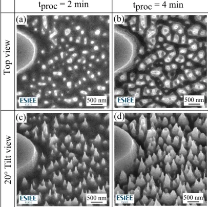
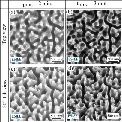
2.2 Time-lapse cryo-DRIE fabrication of BSi sample S03 . . . 23
2.3 Time-lapse cryo-DRIE fabrication of BSi sample S04 . . . 24
2.4 FIB-SEM nanotomography BSi sample orientations . . . 25
2.5 Flowchart for conventional three-dimensional reconstruction by FIB nanotomography . . . 26
2.6 SEM micrographs registration for sample movement during FIB nanotomography 26 2.7 Pair-wise SEM micrographs subtraction to enhance etching boundary . . . 27
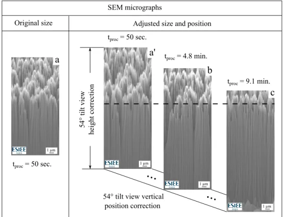
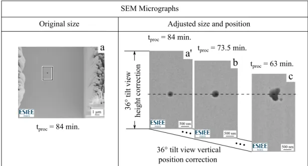
2.8 SEM micrographs 54◦ tilt-view size and vertical position correction . . . 28
2.9 BSi height data triangulation . . . 29
2.10 SEM micrograph of BSi sample S01a during conventional FIB-SEM process . . . 30
2.11 Three-dimensional reconstruction of BSi sample S01a with conventional FIB nanotomography . . . 31
2.12 SEM micrograph of BSi sample S01b during conventional FIB-SEM process . . . 33
2.13 Three-dimensional reconstruction of BSi sample S01b with conventional FIB nanotomography . . . 34
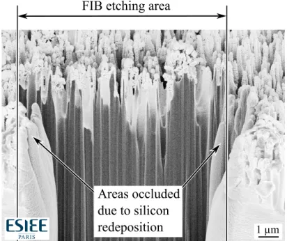
2.14 SEM micrograph of BSi sample S01b during conventional FIB-SEM process showing areas occluded due to silicon redeposition . . . 34
2.15 Image processing of cross-section SEM micrographs using different SEM detectors. 36 2.16 SEM micrographs 36◦ tilt-view size and vertical position correction . . . 37
2.17 SEM micrographs of BSi sample S01c during parallel FIB-SEM process . . . 38
2.18 Three-dimensional reconstruction of BSi sample S01c with parallel FIB nanotomography . . . 39
2.19 Three-dimensional reconstruction of BSi sample S02 with parallel FIB nanotomography . . . 40
2.20 Relation between the SEM micrograph pixel intensity and avg. height obtained from FIB-SEM analysis . . . 42
2.21 Comparison between grey-level analysis and FIB-SEM reconstruction for BSi sample S01 . . . 43
2.22 Three-dimensional reconstruction of initial time-lapse of BSi samples using SEM grey-level analysis . . . 44
2.23 Height histograms of BSi samples . . . 45
2.24 Silicon–air fill factor vs. height of BSi samples . . . 45
2.25 Structure spacing histograms of BSi samples . . . 46
2.26 Topographic parameters evaluation in small regions of BSi sample S02 . . . 48
3.3 Reflectance measurements of BSi samples . . . 55
3.4 Specular reflectance measurements of BSi samples by ellipsometry . . . 56
3.5 Relative permittivity and tangent loss of crystalline silicon obtained by ellipsometry. 57 3.6 Pyramid approximation to an arrangement of variable dielectric constant layers . 58 3.7 Effective permittivity calculation of a pyramid layer based on the synthesized capacitance model . . . 59
3.8 Top-view of BSi model with rectangles delimiting the extracted regions used as periodic unit cell . . . 62
3.9 Reflectance simulations of real surface topography regions . . . 64
3.10 Normalized height distribution comparison between equivalent structure shapes and BSi samples . . . 65
3.11 Reflectance simulations of equivalent structure cells . . . 66
3.12 Top and three-dimensional view of 4 inverted cones multi-structure unit cell . . . 68
3.13 Comparison of normalized heights distributions of equivalent unit cells with BSi height distribution . . . 70
3.14 Reflectance simulations of single and multi-structure unit cells . . . 71
3.15 Specular reflectance simulations and measurements of inverted pyramid structures based on BSi samples hσ . . . 73
3.16 Specular reflectance simulations and measurements of BSi samples real surface topography . . . 74
3.17 Reflectance simulations of single and multi-structure unit cell vs. AOI . . . 75
3.18 Optical simulations and measurements of a polished Si surface and BSi sample S01 77 4.1 Flowchart diagram of BSi formation algorithm. . . 81
4.2 Diagram of passivation layer formation during cryo-DRIE. . . 82
4.3 Actual passivation layer thickness ZPL vs. calculated passivation layer thickness ZPLlin assuming linear growth . . . 83
4.4 Diagram of Silicon etch depth dependence on vpe and vpf . . . 87
4.5 Phase diagram of BSi aspect ratio (AR) dependence on vpe and vpf and cross-sectional views of resulting geometries . . . 88
4.6 Cross-sectional views of simulated and experimental resulting geometries for the BSi formation at different vpf values and O2/SF6 ratios. . . 89
4.7 Silicon content vs. depth comparison between simulated structures and BSi sample S02 . . . 90
4.8 Dynamic study of BSi aspect ratio evolution with time . . . 92
4.9 Time-lapse data showing the evolution of sample S03 . . . 93
4.10 Time-lapse data showing the evolution of sample S04 . . . 94
4.11 BSi formation mechanism . . . 95
4.12 Formation of new etch fronts on saddle points . . . 95
5.1 Minority carrier lifetime vs. minority carrier density for Si wafers samples A and B after passivation process. (Measurement performed at LPICM) . . . 99
5.2 Minority carrier lifetime vs. minority carrier density after passivation and annealing process . . . 99
5.3 BSi solar cell fabrication process . . . 100
5.4 Layout of masks used in the BSi fabrication process . . . 101
5.5 Si wafer doping level profiles obtained by SIMS . . . 103
1.1 Typical range of cryo-DRIE parameters . . . 6 2.1 BSi cryo-DRIE fabrication parameters . . . 20 2.2 Time-lapsed BSi cryo-DRIE fabrication parameters . . . 22 2.3 BSi S01a FIB-SEM etching parameters . . . 30 2.4 BSi S01b FIB-SEM etching parameters . . . 32 2.5 Parallel FIB-SEM etching parameters . . . 38 2.6 Topographic parameters of BSi samples . . . 49 2.7 Time-lapsed BSi samples topographic parameters . . . 50 3.1 Comparison between the topographic parameters of each region with their
corresponding global sample parameters. . . 63 3.2 Mean reflectance calculations of simulations and measurements for single
structure cells based on BSi samples . . . 67 3.3 Multi-structure cell dimensions based on BSi local variation of surface topography 69 3.4 Multi-structure cell dimensions before and after the adjustment for mean and
STD of height . . . 70 3.5 Mean, STD and NRMSE calculations for: single-structure and multi-structure
simulations and BSi sample S02 measurements . . . 72 4.1 BSi Simulation Parameters . . . 93 5.1 Si substrate specifications . . . 98 5.2 Fabrication parameters for minority carrier lifetime measurement . . . 98 5.3 BSi cryo-DRIE fabrication parameters . . . 104
AFM . . . Atomic force microscopy ALD . . . Atomic layer deposition AR . . . Aspect ratio
BSi . . . Black Silicon
cryo-DRIE . . . Cryogenic deep reactive ion etching CVD . . . Chemical vapour deposition
DRIE . . . Deep reactive ion etching FDTD . . . Finite-difference time-domain FEM . . . Finite element method FIB . . . Focused ion beam HAR . . . High aspect ratio
ICP . . . Inductively coupled plasma MEMS . . . Micro-electro-mechanical systems NEMS . . . Nano-electro-mechanical systems NRMSE . . . Normalised root mean squared error PCE . . . Power conversion efficiency
PSD . . . Power spectral density
RCWA . . . Rigorous coupled-wave analysis RF . . . Radio frequency
RIE . . . Reactive ion etching SE . . . Secondary electrons
SEM . . . Scanning electron microscope SIMS . . . Secondary ion mass spectrometry STD . . . Standard deviation
Introduction
Contents1.1 State of the art . . . 1 1.1.1 BSi fabrication . . . 3 1.1.2 BSi applications . . . 7 1.1.3 BSi characterization . . . 10 1.1.4 BSi optical modelling . . . 13 1.1.5 BSi growth modelling . . . 15 1.2 Contributions to the state of the art . . . 16
1.1
State of the art
A large amount of research has been conducted into micro/nano-textured surfaces because of the interesting properties provided by their topography independently of their material composition. Such properties include their optical reflectance and water repelling capability that drastically change in micro/nano-textured surfaces compared to untreated or polished surfaces. It is believed that taking advantage of these properties, they can lead to the improvement of the evolving requirements of miniaturized systems and sensors, as well as solar cells.
By texturing a surface with micro/nano-structures, it is possible to reduce its optical reflectance to low values, below 1%. This reflectance reduction has been studied since several decades in materials such as Silicon (Si), obtained after a texturization process resulting in an array of densely-packed high aspect ratio (AR) micro/nano-structures [3]. The reflectance is reduced when the width of the structures are in the same order of magnitude of the visible
light wavelengths or smaller; this effect can be interpreted as a result of the multiple wave scattering induced by the rugosity diffraction [23] or the smooth transition between the air and the silicon substrate achieved through surface patterning [24]. Many dark surfaces have been produced with different texturing methods such as electro-deposition and sputtering, using different materials other than silicon such as: aluminium, nickel, beryllium, graphite and many others. [25]. Up to this date, the darkest manufactured surface consists of vertically aligned carbon nanotubes with a 0.045% total reflectance reported [26].
Silicon is currently one of the preferred materials used in the development of micro/nano electromechanical systems (MEMS and NEMS), due to its availability and to well-established fabrication processes and modelling techniques. Several forms of micro/nano-textured silicon surfaces with near-zero reflectance have been demonstrated, such as periodic arranged silicon nanopillars patterned with soft-imprint lithography [27], high AR periodic nanowires obtained by a specialized metal evaporation patterning technique [28] and maskless formation of randomly arranged silicon needle-like micro/nano-structures also known as black silicon (BSi) [19].
In contrast to lithography-based patterning techniques, BSi surfaces are the result of a self-patterning generation of disordered needle-like high AR subwavelength structures, obtained at special process conditions on non-masked silicon surfaces. The reflectance of BSi surfaces is reduced over a broad wavelength and angles of incidence range, and the surfaces appear black when directly observed. Due to the submicrometer size of BSi structures, they can only be observed with devices such as a scanning electron microscope (SEM). The shape, dimensions and the spacing of these structures may vary according to the fabrication method used, which also has an effect on the reflectance behaviour at visible light wavelengths as previously demonstrated in simulations and measurements [13, 29].
In this introductory Chapter we review several aspects of BSi surfaces obtained from a thorough bibliography study, such as its fabrication methods, applications, topography characterization methods, modelling techniques for optical simulations, and growth mechanisms. We also describe the contributions that this thesis brings to the state of the art: a better understanding of BSi topography, optical behaviour and insights into its formation mechanism.
1.1.1 BSi fabrication
A wide variety of techniques employed to fabricate BSi have been demonstrated, which can be classified in three general categories: plasma-based etching, wet etching and laser-chemical etching.
1.1.1.1 Plasma-based etching
In plasma-based etching, ions and radicals (formed from gaseous compounds) are projected to the sample to produce reactive etching, ion milling or the combination or both. The different plasma-based etching techniques can be classified according to the method of ions generation, ions acceleration towards the wafer, the gaseous compounds used and the chamber configuration [1]. The first reports of low reflectance surfaces produced by mask-less silicon patterning were obtained by sputtering-etching and reactive ion etching (RIE) [3, 30].
• Conventional Reactive Ion Etching (RIE)
RIE is a plasma-based etching method used in MEMS and integrated circuit (IC) fabrication, where the ions generation and acceleration towards the wafer are controlled with the same radio frequency (RF) power source. There are several combinations of gas compounds used in RIE, one example being the use of sulphur hexafluoride SF6 for silicon etching, oxygen O2 that generates
a conformal passivation layer and fluoroform CHF3 used for the directional passivation layer
etching [19].
In order to find the right amount of each gas flow that provides anisotropic etching with vertical profiles on masked Si wafers, a method was proposed called “the black silicon method” [19], from which the name “black silicon” originated. This method consists of, while maintaining the other process parameters fixed, gradually increasing the oxygen flow until BSi is observed (since BSi is formed in overpassivating regimes), followed by slightly decreasing the oxygen flow until the BSi is not longer observed. The oxygen gas flow obtained when BSi is not longer observed provides the calibration point for vertical profile anisotropic etching.
Based on the influence of the temperature in the anisotropy of the etching profile [31], BSi fabrication by RIE, using SF /O plasmas at low and cryogenic temperatures (cryogenic RIE),
was demonstrated [20, 32].
The molecular interactions during BSi formation in SF6/O2 based plasmas in cryogenic
RIE have been previously described [20, 32]: the plasma mixture produces SF+x ions and F∗ radicals, which diffuse to the substrate producing an isotropic chemical etching reaction on Silicon. Simultaneously, the O∗radicals produced by oxygen also diffuse to the substrate creating a passivation layer SixOyFz that protects the silicon from being etched (the formation of the
passivation layer being enhanced at cryogenic temperatures). While this layer cannot be removed by the F∗ radicals, it is sensitive to physical directional etching by the SF+x ions. Due to the ions’ trajectory, the etching is stronger on horizontal surfaces than on vertical walls. When the passivation layer formation and etching rates are only slightly different (controlled by the SF6/O2 gas flow ratio), the competition between the two processes leads to anisotropic etching
and the formation of high aspect ratio (HAR) structures such as BSi. A schematic of BSi formation process is shown in Figure 1.1.
The initial appearance of BSi structures in a cryogenic RIE process (with gas compounds consisting of SF6/O2/CHF3 or SF6/O2 at cryogenic temperatures) was attributed to
micromasking produced by native oxide and dust, followed by the formation of needles due to the isotropic passivation layer growth combined with directional etching [19, 20].
Figure 1.1. BSi formation by RIE (reproduced from [20]).
Current plasma-based techniques to produce BSi with very high aspect ratios involve the use of an inductively coupled plasma (ICP) RIE chamber (Figure 1.2). In ICP-RIE the generation of ions and their acceleration towards the sample are controlled independently by the ICP RF power and the voltage bias. Two BSi formation methods used with ICP-RIE are: Continuous deep reactive ion etching at cryogenic temperatures (cryo-DRIE) [21, 33] and, respectively, time-multiplexed deep reactive ion etching also called the “Bosch” process (DRIE-Bosch) [34].
In cryo-DRIE, the usual gas compounds consist of SF6 to etch the silicon, O2 that forms
a conformal passivation layer at cryogenic temperatures, and the directional etching of the passivation layer is controlled with the adjustable voltage bias. DRIE-Bosch is, by contrast, performed at ambient temperatures and uses a discretized series of etching and passivation steps: SF6 gas is used in the etching step and octofluoro cyclobutane C4F8 is used in the passivation
deposition step. In the DRIE-Bosch technique, the possibility to adjust the duration of the time steps provides greater control on the anisotropic etching profile; however, the discontinuity between passivation and etching steps may result in a scalloping effect in vertical walls.
Figure 1.2. Schematic of Alcatel cryo-DRIE reactor (reproduced from [35])
While the molecular interactions that produce anisotropic etching and result in the formation of HAR structures in cryogenic RIE also apply to cryo-DRIE, the use of the ICP reactor implies
different process parameters. The cryo-DRIE process parameters with typical values range are summarized in Table 1.1.
Table 1.1. Typical range of cryo-DRIE parameters
cryo-DRIE parameters Typical values
Minimum Maximum Temperature (◦C) -120 30 ICP Power (W) 350 2000 DC bias Voltage (V) -50 0 Pressure (Pa) 1.2 10 O2 flow (sccm) 5 30 SF6 flow (sccm) 100 300
Process Time (minutes) 1 30
Parametric analysis of the different cryo-DRIE parameters have provided information on their influence in the BSi topography, and SEM images observations suggest that the needle-like structures are the residual silicon from the etching of a disordered network arrangement of holes in the substrate [13, 21]. While the holes etching follows the mechanism described previously, the formation of the initial roughness that derives in the final BSi structures has not been yet clearly explained. A link has been suggested between the initial formation of BSi structures and the roughness observed in planar Si surfaces after isotropic plasma etching [36].
1.1.1.2 Wet etching
BSi fabrication by wet etching, as the name suggests, involves the use of a liquid solution to etch the sample combined with customized techniques to achieve the anisotropic etching of submicrometric structures. Initial wet etching silicon texturization techniques consisted in anodic etching of Si substrates in HF solutions to produce a low reflectance porous silicon with nanometric structures [37] and the etching of Si wafers coated with a nanometric gold layer in a HF:H2O2:H2O solution [6, 38]. Variants to these techniques were later reported such as a
pulsed electrochemical etching using a HF:C2H5OH:H2O solution [39], where the topography
can be controlled by adjusting the duration and current density of the pulsed etching process, by replacing the Au deposition with a wet etching step in PdCl2 [40], by controlling the size of
Au particle by liquid-phase chemical reduction method [41], or by coating the Si substrate with HAuCl4 solution instead of evaporated Au deposition [42].
1.1.1.3 Laser-chemical etching
Another Si texturing method that results in an array of micrometric structures has been demonstrated using laser pulses duration of 100 fs and energy density of 10 kJ/m2 [2]. While this method requires the presence of Si etching gases such as SF6 or Cl2, the substrate does
not need to be in vacuum as in plasma etching techniques. The structures obtained by this process consist of cones height of approximately 40 µm and diameter of 1µm. Larger structures (40 µm of height and 20 µm of diameter) can be obtained by using laser pulses of longer duration (30 ns) [43]. Due to sulphur doping and texturization process, BSi samples produced by this technique exhibit greater absorbance with respect to untreated Si substrate [5]. It was later reported that submicrometric and nanometric size structures can be obtained with femto seconds laser pulses by submerging the Si substrate in distilled water during the irradiation process [44, 45].
1.1.2 BSi applications
Since the initial reports on patterning Si to produce low reflectance surfaces [3], an application has been proposed to improve the power conversion efficiency (PCE) of silicon solar cells. Taking advantage of the BSi formation using reactive ion etching (RIE), which is unaffected by the crystalline orientation of the Silicon substrate, a single-junction solar cell using RIE patterned silicon was fabricated on a poly-crystalline Si substrate, with a reported PCE of 17.1%, providing an increase of 0.7% compared to a solar cell with structured surface using photolithography [4]. An increase of the PCE was also demonstrated on poly-crystalline solar cells, based on porous Si surface produced by an anodic etching technique [46]. Due to the BSi low reflectance over a wide range of incident angles, a study suggests, based on current density measurements, that a BSi solar cell can perform better than a conventional solar cell at oblique incident angles, which can be an attractive feature for solar cells without mechanisms to follow the sun trajectory [47, 48]. While BSi-based solar cells perform better than planar solar cells, there are many
challenges that have prevented them from becoming a standard product. First, there is a trade-off between the reflectance reduction and the surface carrier recombination levels that limits the structures height to a small range for optimal PCE [49, 50]. Second, the increase of the surface area caused by the BSi structures increases the sheet resistance when using shallow junctions therefore increasing power losses [32]. Several attempts to overcome these challenges have provided important improvements in the PCE, such as a wet-etching step (damage removal etching) after RIE patterning in order to increase the minority carrier lifetime of the surface [51], yielding a PCE of 17.6% [52]. Measurements of the current density in solar cell with different nano-structure dimensions show the possibility to overcome the losses caused by surface recombination when using periodic silicon nanowires [53]. Another approach is to avoid the losses caused by the front surface recombination by placing the junction on the back surface of the substrate [54]. Recent improvements in the PCE were obtained in BSi solar cells based on metal-assisted chemical etching on crystalline Si wafers, with a PCE reported of 18.2% [55]. The high surface recombination levels observed in textured cells are partially attributed to conventional passivation layer deposition techniques that are not conformal to the structure shape. Measurements of high minority carrier lifetime on BSi with a conformal passivation layer (Al2O3) applied by atomic layer deposition (ALD) show a great potential for
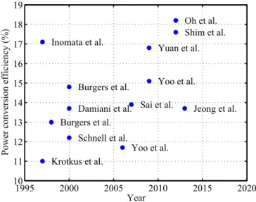
improved PCE in BSi solar cells [56]. Figure 1.3 summarizes the PCE obtained from textured silicon solar cells in the last decades.
In addition to the low reflectance at visible wavelengths that is obtained by patterning silicon, another interesting property reported is the increase of the absorption coefficient in both visible light and near infrared wavelengths [5]. The ability to absorb more light in thinner wafers provides new techniques to design thin films solar cells to reduce fabrication cost [6]. A great improvement in the near infrared sensitivity by using BSi based photodetector was demonstrated [7]. While the increase of the surface absorption coefficient is partially due to the surface texturization, the substrate doping level plays in important role when absorbance near to unity values are required. The substrate doping level can be increased in the front surface during the texturization process, resulting in absorbance greater than 90% (for a wavelength range between 0.4 µm and 2.5 µm) [60]; higher absorbance (greater than 99% for wavelength range
Figure 1.3. Power conversion efficiency evolution of BSi based solar cells in the last decade (Inomata et al. [4], Krotkus et al. [46], Burgers et al. [49], Burgers et al. [57], Damiani et al. [50], Schnell et al. [32], Yoo et al. [58], Sai et al. [48], Yoo et al. [51], Yuanet al. [59], Shim et al. [52], Oh et al. [55], Jeong et al. [54]).
between 0.25 µm and 2.25 µm) are obtained when using heavily doped silicon substrates [61]. Based on measurements of catalytic activity, BSi structures increase the surface area to more than 10 times with respect to a planar surface [8], which implies that BSi surfaces have great potential applications in the miniaturization of devices used for catalytic reactions and sensing. A capacitor fabricated with textured electrodes, having a surface area enhancement of 2, increased its capacitance by 30% when compared to a capacitor with planar electrodes of same dimensions [62]. BSi-based biosensors have been demonstrated with the development of a highly sensitive glucose detector based on nano-textured silicon [63] and a BSi-based surface enhanced Raman spectroscopy detector for algae cells [64]. BSi surfaces have also been used to enhance the surface activity in catalytic microreactors [8] and fuel cells electrodes [65]. Other biological applications of BSi surfaces such as a support for entrapping kidney cells have been demonstrated [66].
Due to its complex topography that consists of dense high aspect ratio structures, BSi has been a fast and convenient technique to create super-hydrophobic surfaces with many applications such as self-cleaning mechanisms [9] and as a support for liquid droplets used in microelectromechanical sensors [10], electrostatic actuators [11] and optical systems [12]. The
air pockets between the structures provide an enhanced contact angle of water droplets with values greater than 170◦ reported [67]. In addition, BSi structures can be either super-hydrophilic by creating a SiO2 layer with O2 based plasma or super-hydrophobic by
creating a teflon-like layer with C4F8 based plasma. Complex droplet shapes can be created by
combining the two processes on the sample surface [68]. BSi fabricated with Bosch process exhibits super-hydrophobicity without any further treatment due to the use of C4F8 as a
passivation agent [69].
Despite the nanometric dimensions of BSi structures, they have a considerable mechanical resistance allowing the use of BSi surfaces as a reversible bonding material showing retention forces greater than 1000 N/cm2 [70].
Only recently, works related to self-cleaning solar cells by combining both the low reflectance surface and hydrophobic properties provided by a lithography nano-patterning of the surface has been proposed [9]. Self-cleaning solar cells have great potential for applications in remote locations, such as small cells installed in street lights in arid climates, where maintenance is difficult or expensive. Studies of the power efficiency decrease due to dust accumulations have been previously performed [71, 72], where reductions of the PCE by 17.4% per month has been reported due to dust deposition on 45◦ tilted solar cells [71].
1.1.3 BSi characterization
As previously mentioned, the characterization of the nanometric-sized structures of BSi samples requires specialized microscopy techniques such as imaging with a scanning electron microscope (SEM). Compared to other microscopy techniques such as field-ion and atom-probe, SEM is a more appropriate method for BSi structures visualization and characterization due to its combination of large image scanning size, good resolution and it is a non-destructive technique. While atomic force microscope (AFM) could also be used for BSi visualization, samples having high aspect ratio such as BSi, cannot be accurately observed due to the limited angle of AFM tips which prevent them from reading the bottom of the structures. In this Section we will present the current methods employed to characterize and to obtain accurate three-dimensional representations of HAR nanostructures such as BSi.
1.1.3.1 SEM imaging
The SEM allows the observation of metallic or semiconductor surfaces at very small scale (images of resolution less than 10 nm and size more than 20 x 20 µm). The sample to be analysed is placed in a high-vacuum chamber where it is bombarded with a fine electron beam that scans the sample surface. While the sample is bombarded with electrons, some of them are back scattered and others interact with the sample producing secondary electrons. Different detectors placed in the chamber allow to collect these backscattered and secondary electrons and convert them into an electric signal which is then converted to an image based on the quantity of electrons detected per sampled area. The advantage of using SEM to observe irregular surfaces is that the quantity of secondary electrons detected depends of the local tilt angle of the surface allowing us to observe images (also called micrographs) that represent the topography of the surface. Although several types of signals can be detected with SEM, in this manuscript we focus in the in-lens and Everhart-Thornley (SE2) secondary electron detectors.
The difference between the in-lens and the SE2 detector being their location, the former detects secondary electrons that are emitted back to the same direction of the electron beam, and the latter detects secondary electrons that are emitted to one side of the chamber. The location of the detectors affects the illumination appearance of the SEM micrographs, so the illumination of an in-lens micrograph appears to occur from the same axis of the observer’s line of sight and the illumination, whereas the illumination of a SE2 micrograph appears to occur at a tilted angle of the observer’s line of sight [73].
Another feature of the SEM imaging is that the amount of secondary electrons detected in irregular surfaces depends on the surface occlusion or exposure solid angle, meaning that structures that are highly exposed to the electron beam will appear brighter than areas that are highly occluded due to surrounding structures (such as the bottom of holes in BSi). This effect can be observed with both in-lens and SE2 detectors and is the feature that allows inferring the structure height as function of the top-view SEM pixel intensity.
Since the initial reports on subwavelength structures in silicon, SEM has been the most utilized method to characterize the topography of BSi samples. Top-view micrographs of the
sample can be used to estimate the diameter and the average spacing of the structures, cross-section views allow the estimation of the height of the structures and tilted views of the samples provide a general idea of the structures’ shape and uniformity. The aspect ratio of the structures is deduced from both the height and diameter of the structures.
In previous studies where characterizations of BSi structures were made, the measurement of the average height, diameter and structure spacing is based on SEM images at different viewing angles [13]. The measurement of height based on cross-section view of SEM micrographs can be misleading due to the dense agglomeration of structures and the non-uniform nature of BSi topography that cannot be observed from a single cross-section micrograph. Three-dimensional reconstruction methods can be employed to obtain an accurate representation of the structures height.
1.1.3.2 SEM grey-scale analysis
SEM grey-scale analysis is a reconstruction technique from which a three-dimensional model that represents the surface topography of BSi samples can be obtained. This method consists of inferring the structures height based on the grey-scale level of a top-view SEM image, using the known height values of the SEM brightest and darkest grey-level as bounds of an interpolating range. While other non-destructive methods of reconstruction such as the ones based on multiple images taken at different viewing angles have been demonstrated, they require repositioning the sample at different viewing angles and robust algorithms to detect the same features in the different images [74].
SEM grey-scale analysis has been effectively used in the reconstruction of BSi samples [14]; however, there are some limitations of the maximum hole depth detectable that are due to the limited SEM dynamical range. Therefore, while the SEM grey-scale analysis provides accurate topography information, it is limited to BSi samples with small or medium aspect ratios.
1.1.3.3 FIB-SEM nanotomography
FIB-SEM nanotomography, or serial sectioning, combines the controllable etching capabilities of the focused ion beam (FIB) and the non-destructive imaging capabilities of the
SEM in a single process. It consists of alternating steps of FIB etching and SEM image acquisitions performed on a sample in order to obtain a series of cross-section images at different etching levels. Further processing of this stack of images allows the reconstruction of a three-dimensional representation of the sample. This technique provides a nanometric resolution of the same order of the SEM image (<10 nm with sample size of >20 x 20 µm) along two axes, and the third axis resolution depends of the etching step length (∼10 nm) and the SEM micrograph acquisition interval. FIB-SEM analysis has been used in many applications such as the characterization of metal alloys, granular and porous surfaces, reconstruction of biological tissue, and others [15].
BSi topographical reconstruction using FIB-SEM analysis implies a simpler procedure than the previous mentioned applications since it consists of a single material without air inclusions or overhanging structures. However, due to the lack of contrast difference between the etched and non-etched material a FIB-assisted metal deposition step (usually Platinum) is applied before the FIB-SEM analysis procedure [75]. Additional preparation steps are required such as etching the material surrounding the area to be analysed [76] and the formation of horizontal alignment marks to have a feedback on the amount of material etched between steps, which is also used to calculate the displacement caused by the tilted positioning [77].
1.1.4 BSi optical modelling
Optical modelling of subwavelength structures is a crucial step to find the optimal topographic parameters that provide reduced reflectance, increased absorbance and that meet additional constrains imposed by the application. The topographic parameters necessary for BSi optical modelling are the structure shape, height, diameter, spacing and surface area enhancement factor. One example of a constraint imposed by the application is the surface area enhancement factor in solar cells applications, which has to be kept to a minimum in order to avoid excessive surface recombination that leads to a reduced minority carrier lifetime. The contrary is true in light absorbers used in devices such as telescopes and other optical instruments, where the objective is to reduce reflectance to a minimum regardless of the topography, therefore samples with enhanced surface area can be used.
While optical modelling of BSi samples can provide general guidelines of the best topographical parameters for the application, due to constraints imposed by the cryo-DRIE fabrication process the optimal topography parameters cannot always be achieved. Therefore, it is a common practice to numerically simulate the optical parameters of models based on already fabricated samples, which are then validated with measurements, to find the fabrication parameters that provide the most appropriate BSi sample for the application.
From the various methods of modelling the optical parameters of textured samples, the most utilized are the finite difference time domain (FDTD) method, the finite element method (FEM) and rigorous coupled wave analysis (RCWA). Each method has its advantages and limitations but in general all three methods are capable of calculating optical parameters such as total reflectance, transmittance and absorbance on arbitrary three-dimensional structures. In order to simulate micro/nano-textured surfaces with any of these methods, they require the modelling of a unit cell that represents a typical structure shape that is present in the surface, such as cylinder, pyramid cone, etc. Periodic boundaries are imposed in this unit cell in order to represent an infinite array of structures. The second requirement for optical modelling is to provide the material bulk complex relative permittivity and permeability in function of frequency. When the micro/nano-textured surface is aperiodic with a strong variation of the topographic parameters along the surface (such as BSi), an unit cell can be modelled with a portion of the surface topography [16, 17], however the unit cell dimensions might be limited by the computational resources available in certain numerical methods. Another approach to solve the optical parameters of an aperiodic structure is to model an artificial equivalent single cell that is deduced from a statistical analysis of a large region of the surface and takes in account the variations of the topographical properties [18].
Both FDTD and FEM are numerical modelling methods, based on a discretization of the geometry into a mesh of volumetric elements, capable to solve the Maxwell’s equations to obtain the electromagnetic field quantities. The total reflectance, transmittance and absorbance are deduced from the electromagnetic field. Previous reports on simulated optical parameters of nanostructured surfaces using the FDTD method demonstrate a good agreement with measurements. Examples of such reports are the total reflectance simulations of single