HAL Id: tel-00507494
https://tel.archives-ouvertes.fr/tel-00507494
Submitted on 30 Jul 2010HAL is a multi-disciplinary open access archive for the deposit and dissemination of sci-entific research documents, whether they are pub-lished or not. The documents may come from teaching and research institutions in France or
L’archive ouverte pluridisciplinaire HAL, est destinée au dépôt et à la diffusion de documents scientifiques de niveau recherche, publiés ou non, émanant des établissements d’enseignement et de recherche français ou étrangers, des laboratoires
High-Efficiency Self-Adjusting Switched Capacitor
DC-DC Converter with Binary Resolution
Alexander Kushnerov
To cite this version:
Alexander Kushnerov. High-Efficiency Self-Adjusting Switched Capacitor DC-DC Converter with Binary Resolution. Electronics. Ben-Gurion University of the Negev, 2010. English. �tel-00507494�
FACULTY OF ENGINEERING SCIENCES
HIGH-EFFICIENCY SELF-ADJUSTING
SWITCHED CAPACITOR DC-DC CONVERTER
WITH BINARY RESOLUTION
by
Alexander Kushnerov
A thesis submitted to
the Department of Electrical Engineering and Computer Science
in partial fulfillment of the requirements
for the degree of
Master of Science
Supervised by: Professor Sam Ben-Yaakov
and
Professor Eugene Paperno
Intellectual Property
Copyright © 2009 by the author(s)
No part of this work may be used for profit or commercial advantage without the prior written consent of the copyright proprietor(s). Reproduction of any part of this work is permitted for personal use or educational purposes only, provided the source is properly referred.
All rights reserved. Patent pending
High-Efficiency Self-Adjusting Switched Capacitor DC-DC Converter with Binary Resolution
A thesis for the degree of Master of Science
by
Alexander Kushnerov
Dipl. Ing. (Omsk State Technical University) 2002 Defense place and date:
Ben-Gurion University of the Negev, March 4, 2010 Jury:
Professor Sam Ben-Yaakov Professor Eugene Paperno Professor Raul Rabinovici Doctor Doron Shmilovitz
A
BSTRACTSwitched-Capacitor Converters (SCC) suffer from a fundamental power loss deficiency which make their use in some applications prohibitive. The power loss is due to the inherent energy dissipation when SCC operate between or outside their output target voltages. This drawback was alleviated in this work by developing two new classes of SCC providing binary and arbitrary resolution of closely spaced target voltages. Special attention is paid to SCC topologies of binary resolution. Namely, SCC systems that can be configured to have a no-load output to input voltage ratio that is equal to any binary fraction for a given number of bits.
To this end, we define a new number system and develop rules to translate these numbers into SCC hardware that follows the algebraic behavior. According to this approach, the flying capacitors are automatically kept charged to binary weighted voltages and consequently the resolution of the target voltages follows a binary number representation and can be made higher by increasing the number of capacitors (bits). The ability to increase the number of target voltages reduces the spacing between them and, consequently, increases the efficiency when the input varies over a large voltage range.
The thesis presents the underlining theory of the binary SCC and its extension to the general radix case. Although the major application is in step-down SCC, a simple method to utilize these SCC for step-up conversion is also described, as well as a method to reduce the output voltage ripple. In addition, the generic and unified model is strictly applied to derive the SCC equivalent resistor, which is a measure of the power loss. The theoretical predictions are verified by simulation and experimental results.
ACKNOWLEDGEMENTS
First and foremost, I would like to thank my advisor Professor Sam Ben-Yaakov for his patient guidance. He gave me a chance to start my education here and provided a very good environment for my research and study. Besides his outstanding expertise in both theoretical and practical matters, his amicable disposition and accessibility have provided for constructive and fruitful work. Professor Ben-Yaakov has taught me how to structure my ideas more rigorously and I believe over these past years that I have absorbed some of his creative approach to research.
This thesis could not have been developed without the pioneering work and continual support of Meir Shashoua, co-founder of "K. S. Waves Ltd.", Tel-Aviv, Israel. I am grateful to Mr. Shashoua for his original ideas and asking questions that have periodically resurfaced in my mind and conducted me to sharper thinking. The material assistance from "K. S. Waves Ltd." is deeply appreciated and deserves special acknowledgement.
I am greatly indebted to the graduate student Michael Evzelman for his friendship and optimism. He is always ready to discuss anything that could be connected with motorcycles, electronics or programming. My gratitude is also to Alexei Smirnov, the author of the NL5 circuit simulator, for his careful reading of the manuscript and help with English corrections.
At the end of this study I wish to thank my mother – her love, understanding, support and sacrifices are always an encouragement to me.
TABLE OF CONTENTS
Page 1. INTRODUCTION
1.1 Background review . . . 10
1.2 Motivation and relevance . . . 12
2. BASICS OF SWITCHED CAPACITOR CIRCUITS 2.1 Transient and limitation of current spike. . . 13
2.2 Inherent energy loss at voltage difference . . . 19
2.3 Target voltages and SCC equivalent circuit . . . 21
2.4 Demystifying the equivalent resistor issue . . . 23
3. PROPOSED CLASSOF SCC WITH BINARY RESOLUTION 3.1 Extended binary (EXB) representation . . . 27
3.2 Spawning the EXB codes and its corollaries . . . 29
3.3 Combinatorial method for obtaining EXB codes . . . 31
3.4 Translating EXB codes to SCC topologies . . . 33
3.5 Self-adjusting voltages in EXB based SCC . . . 35
3.6 Method to reduce output voltage ripple . . . 40
3.7 EXB based SCC in step-up mode . . . 42
3.8 Some investigations into redundancy . . . 44
4. PROPOSED CLASSOF SCC WITH ARBITRARY RESOLUTION 4.1 Generic fractional (GFN) representation . . . 46
4.2 Spawning the GFN codes and its corollaries . . . 48
4.3 Combinatorial method for obtaining GFN codes . . . 50
4.4 Translating GFN codes to SCC topologies . . . 52
4.5 Self-adjusting voltages in GFN based SCC . . . .. . . 55
TABLE OF CONTENTS
(cont’d)Page 5. PROPOSED NUMERICAL ANALYSIS
5.1 Investigating the voltage convergence issue . . . 62
5.2 Derivation of the equivalent resistor expressions . . . 71
6. SIMULATION RESULTS 6.1 Verification of equivalent resistor values . . . 78
6.2 Utilizing the EXB based SCC in step-up mode . . . 83
6.3 Test for unipolar voltages across switches . . . 85
7. EXPERIMENTAL RESULTS 7.1 Response to a step in input voltage . . . 91
7.2 Response to a step in load resistance . . . 92
7.3 Efficiency versus load resistance . . . 94
7.4 Load characteristics and effect of Req. . . 95
7.5 Output voltage regulation . . . 99
8. DISCUSSIONAND CONCLUSIONS . . . 101
BIBLIOGRAPHY
APPENDIX A. Circuit diagrams APPENDIX B. Program listings
LIST OF FIGURES
Page
Figure 2.1.1: Switched circuits including ideal capacitors . . . 13
Figure 2.1.2: Switched circuits including serial resistor . . . 14
Figure 2.1.3: Complete response of the charging circuit and its components . . . 16
Figure 2.1.4: A large and fast decaying i(t) and an equivalent impulse . . . . . . 16
Figure 2.1.5: Complete response of the discharging circuit and its components . . . 18
Figure 2.3.1: The output characteristics of a commercial SCC . . . 21
Figure 2.3.2: The SCC equivalent circuit . . . 22
Figure 2.4.1: Voltage follower SCC . . . 23
Figure 2.4.2: Two non-overlapping clocks φ1 and φ2 . . . 23
Figure 2.4.3: Generic charge/discharge circuit . . . 24
Figure 2.4.4: Functions coth β
2 and coth β
2 . . . 26Figure 3.3.1: Full factorial design EXB matrix of size 27×3 and used vectors . . . 32
Figure 3.4.1: SCC topologies configured from the EXB codes of M3 = 3/8 . . . 33
Figure 3.5.1: Topologies of the voltage halving SCC . . . 35
Figure 3.5.2: SCC topologies configured from the EXB codes of M3 = 3/8 . . . 36
Figure 3.5.3: The perpetual EXB sequences of the SCC with M3 = 3/8 . . . 39
Figure 3.7.1: Topologies of the step-up SCC reciprocal to the case of M3 = 3/8 . . . 42
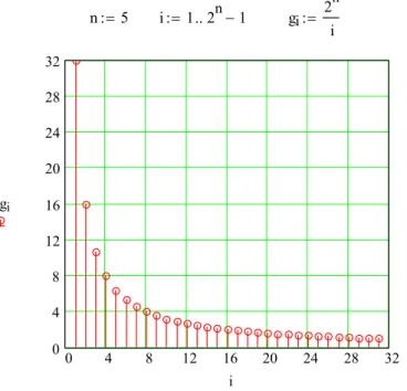
Figure 3.7.2: Step-up conversion ratios 1/Mn, n = 1…5 . . . 43
Figure 4.3.1: Full factorial design GFN matrix of size 25×2 and used vectors . . . 51
Figure 4.4.1: SCC topologies configured from the GFN codes of N1(3) = 3/9 . . . 53
Figure 4.4.2: SCC topologies configured from the GFN codes of N2(3) = 4/9 . . . 54
Figure 4.5.1: Topologies of the SCC with the conversion ratio 1/3 . . . 55
Figure 4.5.2: SCC topologies configured from the GFN codes of N2(3) = 4/9 . . . 56
LIST OF FIGURES (cont’d)
Page
Figure 4.6.1: Topologies of the step-up SCC reciprocal to the case of N2(3) = 4/9 . . . 60
Figure 4.6.2: Step-up conversion ratios 1/Nn(3), n = 1…3 . . . 61
Figure 5.1.1: Topologies of the SCC with the conversion ratio M3 = 3/8 . . . 63
Figure 5.1.2: Convergence of the voltages V1, V2, V3 at zero initial conditions. . . 66
Figure 5.1.3: Convergence of the output voltage at zero initial conditions . . . 66
Figure 5.1.4: Decaying to zero charge at zero initial conditions . . . 66
Figure 5.1.5: The voltages V1, V2, V3 returning to binary weighted initial values . . . 67
Figure 5.1.12: Convergence of Vo when C1, C2, C3 are changed to be binary weighted . . . 70
Figure 5.2.1: Exponential and average currents on a time interval . . . 71
Figure 5.2.2: Charge balance for a single flying capacitor . . . 72
Figure 5.2.3: Topologies of the SCC with the conversion ratio M3 = 3/8 . . . 72
Figure 5.2.4: Switches used in each topology of the EXB based SCC with M3 =3/8 . . . 74
Figure 6.1.1: Double-bridge cascade . . . 78
Figure 6.1.2: Simulation circuit for the EXB based SCC . . . 79
Figure 6.1.3: Switch sub-circuit . . . 79
Figure 6.1.4: Simulation result for M1 = 4/8 . . . 80
Figure 6.1.5: Simulation result for M3 = 1/8 (a) and M3 = 7/8 (b) . . . 80
Figure 6.1.6: Simulation result for M2 = 2/8 (a) and M2 = 6/8 (b) . . . 80
Figure 6.1.7: Simulation result for M3 = 3/8 (a) and M3 = 5/8 (b) . . . 81
Figure 6.1.8: The SCC equivalent circuit . . . 81
Figure 6.2.1: Simulation circuit for the step-up case . . . 83
Figure 6.2.2: Simulation result for 1/M3 = 8/3 (a) and 1/M3 = 8/5 (b) . . . 84
Figure 6.3.1: Measuring the voltages across the switches . . . 85
LIST OF FIGURES (cont’d)
Page
Figure 6.3.4: Measured voltages for M2 = 2/8 (a) and M2 = 6/8 (b) . . . 88
Figure 6.3.5: Measured voltages for M3 = 3/8 (a) and M3 = 5/8 (b) . . . 89
Figure 7.1.1: The SCC cold start, M3 = 3/8, Co = 470µF (a) and Co = 22µF(b) . . . 91
Figure 7.1.2: The SCC cold start, M3 = 5/8, Co = 470µF (a) and Co = 22µF (b) . . . 91
Figure 7.2.1: The SCC response, M3 = 3/8, Co = 470µF, Ro = 128Ω (a) and Ro = 62Ω (b) . . 92
Figure 7.2.2: The SCC response, M3 = 3/8, Co = 22µF, Ro = 128Ω (a) and Ro = 62Ω (b) . . . 92
Figure 7.2.3: The SCC response, M3 = 5/8, Co = 470µF, Ro = 128Ω (a) and Ro = 62Ω (b) . . 93
Figure 7.2.4: The SCC response, M3 = 5/8, Co = 22µF, Ro = 128Ω (a) and Ro = 62Ω (b) . . . 93
Figure 7.4.5: Experimental result for M3 = 3/8 (a) and close-up (b) . . . 96
Figure 7.4.6: Experimental result for M1 = 4/8 (a) and close-up (b) . . . 97
Figure 7.4.7: Experimental result for M3 = 5/8 (a) and close-up (b) . . . 97
Figure 7.4.8: Experimental result for M2 = 6/8 (a) and close-up (b) . . . 97
Figure 7.4.9: Experimental result for M1 = 7/8 (a) and close-up (b) . . . 98
Figure 7.5.1: Dithering between M3 = 3/8 and M1 = 4/8 (in 4:1 ratio) . . . 99
Figure 7.5.2: Output ripple. Dithering between M3 =3/8 and M1=1/2 . . . 99
Figure 7.5.3: Block diagram of output voltage regulation by LDO at the output . . . 100
1. INTRODUCTION
1.1 Background review
The purpose of a DC-DC converter is to provide a predetermined and constant output voltage to a load from a poorly specified or fluctuating input voltage source. Linear regulators and switching converters are two common types of DC-DC converters. In a linear regulator the output current comes directly from the power supply, therefore the efficiency is approximately defined as the ratio of the output voltage to supply voltage. It is obvious that a worse efficiency will be obtained when the supply voltage is much larger than the output voltage. Switching converters are more efficient than linear regulators due to intercepted energy transfer. This is done by periodically switching energy storing components to deliver a portion of energy from the power supply to the output. Switching DC-DC converters (except for resonant converters) can be divided into two large groups: inductive and capacitive.
The inductive converters using one or several inductors have been a power supply solution in all kinds of applications for many years due to the wide variety of possibilities in current and voltage requirements. Generally, the inductors in such a converter are bulky, not realizable on-chip and are the cause of two difficult problems. One problem are high voltage spikes that must be damped or recuperated otherwise, the switches which are not rated for such constraints can blow, while the rest of circuit can be damaged. The other problem with inductive converters is a pulsating input current, which can produce an electromagnetic interference (EMI) from other equipment and conductor lines. This interference may penetrate into susceptible devices and lead to unreliable operation. So, the pulsating input current requires a special filter and sometimes shielding. All these factors increase the board space and inductive converter cost. The capacitive converters based on switched capacitors are widespread in applications requiring small power and no isolation between input and output. They feature relatively low noise, minimal radiated EMI, and in most cases are fabricated as integrated circuits which have made capacitive converters popular for use in power management for mobile devices. An additional goal of such converters is the option for unloaded operation with no need for dummy loads or complex control. However, capacitive converters suffer from inherent power loss during
capacitor. Theory predicts that this power loss is proportional to the squared voltage difference taking place before the corresponding circuit has been configured. As a result, capacitive converters exhibit a rather high efficiency if the capacitors pre-charged to certain voltages are paralleled with components maintaining similar voltages.
The most known type of capacitive DC-DC converter is called a charge pump; for historical reasons it is often considered to a step-up converter built from capacitors and diodes, which are used as switches. Nowadays, when charge pumps are built around transistor switches, their circuitry does not differ in principle from the step-down switched capacitor DC-DC converters. The cornerstone of both circuits is a reconfigurable array of switches and capacitors generally called “flying capacitors”. These capacitors are charged from the input voltage and then discharged to the load thus providing charge transfer and a constant output voltage.
It is a well-known phenomenon that when a capacitive converter operates at the target output to input voltage ratios, the efficiency is high and may exceed 90%. This is due to the fact that, at these voltage ratios, the capacitors do not see appreciable voltage variations. When the same capacitive converter operates between or outside the target voltage ratios, the efficiency drops dramatically. Obviously, in practice one would expect the conversion ratio to change and hence there is no way to escape the losses. However, there are several "lossless" techniques to provide regulation of the output voltage. In most cases, these techniques change the rate at which the charge is transferred to the output and this leads to an increased output voltage ripple. In general, capacitive converters feature a set of discrete target voltage ratios that can be contrasted with the continuous transfer function of inductive converters.
The down side of capacitive converters is the larger number of switches and respective drivers complicating the converter circuitry. Another problem of capacitive converters is a high inrush current during start-up that must be limited by soft-start circuitry.
1.2. Motivation and relevance
“Discontent is the first necessity of progress.”
Thomas A. Edison
Switched Capacitor Converters (SCC) suffer from a fundamental power loss which is a severe limitation because of the common requirement to regulate output voltage. The power loss is due to the inherent energy dissipation when a capacitor is charged or discharged by a voltage source or another capacitor [1-8]. Hence, SCC exhibit rather high efficiency only when operating at the target voltages at which the voltage differences that charge and discharge the capacitors are small. Earlier studies attempted to overcome the power loss by proposing SCC with an increased number of target voltages [9-14]. However, the common disadvantage of these SCC is that the target voltages are spread apart.
It is thus evident that there is a need and it will be highly advantageous to design a SCC that has a large number of target voltages that are spaced at high resolution over the range of interest and thereby improve the efficiency. Another desired feature is a simple way to increase the resolution only by changing the control scheme. In addition, it would be desirable to obtain a smooth transition from one target voltage ratio to another. It is yet another demand to regulate the output voltage while maintaining high efficiency. It would also be desirable to provide low output voltage ripple over a wide range of target voltage ratios.
This work presents the theory that underlines the operation of the multi-target SCC and allows one to design new SCC satisfying the above requirements. The theory is based on the redundancy of the positional number systems [38-42], which is used to develop two new SCC classes providing binary and arbitrary resolution of target voltages. In these new SCC classes, the flying capacitors are automatically kept charged to radix-r-weighted voltages, while the gap between neighboring target voltages is defined by the resolution. Both the radix and the resolution can be made higher by increasing the number of flying capacitors.
2. BASICS OF SWITCHED CAPACITOR CIRCUITS
2.1 Transient and limitation of current spike
“The immediate effect is likely to be what it's always been - a spike in violence.”
Donald Rumsfeld
The principle of a gradual change of energy in any physical system, and specifically in an electrical circuit, means that the energy stored in electric or magnetic fields cannot change instantaneously [1-3]. For the sake of simplicity, however, the assumption is made in transient analysis that the switching occurs quite instantaneously [4-8].
Let t0 be the instant of time when switching starts, and two additional instants: just prior and just after switching be t 0 and t 0 respectively. In mathematical language, the value of the function f(0) is the "limit from the left", as t approaches zero from the left, while
) 0
(
f is the "limit from the right", as t approaches zero from the right. According to the above principle, the voltage (charge) of a capacitor just after switching is equal to the voltage (charge) just prior to switching:
) 0 ( ) 0 ( C C v v (2.1.1) ) 0 ( ) 0 ( q q (2.1.2)
Defining an ideal switch as a zero-resistance device that gets opened or closed in zero time, we consider the charging circuit shown in Fig. 2.1.1(a), where the voltage source VS, the
switch Sw and the capacitor C1 are ideal. When Sw is turned-on, the capacitor voltage v1 changes
abruptly from zero to VS. In other words, the charging of C1 is accompanied by an infinitely high
current pulse during an infinitesimal time.
(a) (b)
Using the above designations, we can write v1(0)0, v1(0)VS and v1(0) v1(0)
which contradicts (2.1.1). In transient analysis, the last expression is called an incorrect initial condition for the chosen mathematical model of an ideal switched circuit.
Consider now the switched circuit of Fig. 2.1.1(b), where the ideal switch Sw serves to discharge the ideal capacitor C1 pre-charged to the voltage v1(0)VS into another empty ideal
capacitor C2. According to the law of charge conservation, the total charge on two capacitors C1
and C2 connected in parallel is the sum of the initial charges q1(0)C1VS and q2(0)0, while
the final voltages are:
S V C C C v v 2 1 1 2 1(0) (0) (2.1.3)
So, the contradiction of vC(0)vC(0) is observed again and, as in the previous case,
the discharging of C1 will be accompanied by an infinitely high current pulse during an
infinitesimal time. This contradiction can be refuted since any circuit with a real capacitor has in practice some resistance and inductance connected in series. The series inductance is generally and is neglected in present analysis.
The infinite current spike is prevented in the switched circuits shown in Fig. 2.1.2, so that the initial conditions are correct. Note that such circuits may be composed by taking into consideration just the resistances of the connecting wires.
(a) (b)
Figure 2.1.2: Switched circuits including the serial resistor.
The charging circuit with the resistor is shown in Fig. 2.1.2(a), it is described by a first order differential equation because it comprises only one capacitor C1. So, the aim is to calculate
the complete response of the first order circuit to the voltage step VS. According to the Kirchhoff Current Law iR(t)iC1(t), this is:
dt t dv C R t v VS ( ) 1( ) 1 1 (2.1.4)
Rearranging the above equation: dt RC V t v t dv S 1 1 1 1 ) ( ) ( (2.1.5)
Now it can be simply integrated:
D dt RC V t v t dv S
1 1 1 1 ) ( ) ( (2.1.6)The integration of both sides yields:
D RC t V t v S 1 1( ) ] ln[ (2.1.7)
Since the time constant RC1,
t D S e V t v( ) 1 (2.1.8)
An initial voltage across C1 will be
S D V
e V
v1(0) 0 (2.1.9)
So, the complete response is:
) 1 ( ) ( 0 1 t S t V e e V t v (2.1.10)
Note that the first term in (2.1.10) is the natural response, while the second term is the forced response. Both terms and the complete response were calculated in MathCAD and are
presented in Fig. 2.1.3 together with the following current, which is limited by I0
VS V0
/R.The time constant may be easily found from Fig. 2.1.3 by drawing a tangent line to the response curve at t 0. The intercept point of the tangent and the asymptotic limit projected to the time axis yields the time constant. The units of the time constant are seconds [τ] = Ω ·F, therefore it is considered as an interval during which the voltage drops (grows) relatively to its initial value. At the end of the τ interval, the voltage is e1 0.368 of its initial value, while at
the end of 5τ the voltage ratio is less than 0.01. Because of this fact, it is usual to presume that the duration of the transient response is about 5τ. Note that, precisely speaking, the transient response declines to zero in infinite time, since et 0, when t .
Vs 1 V0 0.5 Vs R1 C1 10 6 R C1 n5 j n 104 t0 j n up t( ) Vs 1 exp t dn t( ) V0 exp t v1 t() up t() dn t() i t( ) Vs V0 R exp t 0 5 107 1 106 1.5 106 2 106 2.5 106 3 106 3.5 106 4 106 4.5 106 5 106 0 0.14 0.29 0.43 0.57 0.71 0.86 1 v1(t) - voltage across C1 s1(t) - tangent line to v1(t) i(t) - current through R up(t) - forced response dn(t) - natural response v1 t() s1 t() i t( ) up t( ) dn t( ) t
Figure 2.1.3: Complete response of the charging circuit and its components.
When t 5, the voltage v1(t) is considered to be equal to the voltage v1(0)VS as in the ideal switched circuit shown in Fig. 2.1.1(a). The amount of charge transferred by an exponentially decaying current is equal to the product of its initial value and the time constant.
0 0 0 0 0 0
|
) ( ) (t dt I e dt I t e I i q t t
(2.1.11)This result justifies using an impulse function δ to represent the very large, approaching infinity, magnitude of the current pulse, applied for a very short (approaching zero) time interval, whereas their product stays finite, as shown in Fig. 2.1.4.
The other switched circuit with the resistor R is shown in Fig. 2.1.2(b) and serves to discharge the capacitor C1 (pre-charged to the voltage VS) and simultaneously to charge the empty capacitor C2. To find the voltages across these capacitors, consider a bi-directional current
flow and compose two first-order differential equations:
dt t dv RC t v t v dt t dv RC t v t v 2 2 2 1 1 1 2 1 or
dt t dv RC t v t v dt t dv RC t v t v 2 2 1 2 1 1 1 2 (2.1.12)Take the Laplace Transform of both systems:
] 1 [ ] [ 2 2 1 1 1 2 1 RC s s v s v V s v s RC s v s v S
t v s RC s v s v V s v s RC s v s v S 2 2 1 2 1 1 1 2 [ ] (2.1.13)The solutions in the Laplace domain are:
1 2
2 1 2 2 1 1 1 ) ( C C s C C R s RC s V C s v S
2 1 2 1 2 1 2( ) s R CC sC C V C s v S (2.1.14)Taking the Inverse Laplace Transform of both equations (2.1.14), we obtain the voltages in the time domain. To simplify the expressions we introduce the time constant
2 1 2 1 C C C C R
since the current flows through serially connected capacitors.
S S e t C C V C C C V C t v 2 1 2 2 1 1 1
[1 ] 2 1 1 2 S e t C C V C t v (2.1.15) while
S e t R V R t v t v t i 1 2 (2.1.16)The boundary values are:
R V I i S 0 0
2 1 1 1 1 lim C C V C t v V S t
2 1 1 2 2 lim C C V C t v V S t (2.1.17)It is evident from (2.1.16) that the asymptotic limits are the same voltages v1(0+) = v2(0+)
as derived in (2.1.3) by using the charge conservation law. At the instant of switching, the current is limited by i(0)VS /R and reaches 0.01 of this value at 5τ.
As follows from (2.1.14), the transient rates for C1 and C2 are different and defined by the
time constants RC1 and RC2 respectively. Since in this particular case, C1 is pre-charged to VS, its discharging can be considered as the natural response, while the charging of empty C2
matches the definition of a forced response. Both the voltages of (2.1.15) and the current through
R given by (2.1.16) were calculated in MathCAD and depicted in Fig. 2.1.5.
R1 C1 10 6 C2 2 C1 Vs 1 C1 C2 C1 C2 R n5 i n 104 t0 i n v1 t() C1 Vs C2 Vs exp t C1 C2 v2 t() C1 Vs 1 exp t C1 C2 i t( ) v1 t() v2 t() R 0 3.33 1076.67 107 1 106 1.33 1061.67 106 2 106 2.33 1062.67 106 3 106 3.33 106 0 0.17 0.33 0.5 0.67 0.83 1
v1(t) - voltage across C1 (natural response) v2(t) - voltage across C2 (forced response) i(t) - current through R
x(t) - tangent line to i(t) v1 t()
v2 t() i t( ) x t( )
t
2.2 Inherent energy loss at voltage difference
“In mathematics you don't understand things. You just get used to them.” John von Neumann
The transient in the switched circuits considered in the previous section is accompanied by either an infinitely high pulse or an exponentially decaying current. Energy is lost in both cases; however, in each case the nature of energy loss is different. In the first case of the ideal switched circuit, it is common to presume that the energy loss is radiation caused by the infinitely high current pulse. The other case is more close to practice because the current is limited by the series resistor, which is heated and dissipates energy. As known, the energy stored in the capacitor is:
Q V C Q CV E 2 2 2 2 2 (2.2.1)
Consider again the charging circuit in Fig. 2.1.1 (a), where the ideal capacitor C1 is
pre-charged to the voltage V0 and holds an initial energy E0 C1V02 2. After C1 is charged instantaneously to VS, the final energy E1C1VS2 2 and the voltage difference V VS V0, its
square defines the energy loss:
2 2 1 0 1 V C E E E (2.2.2)The same energy is dissipated as heat when the capacitor C1 is charging through the
resistor R as shown in Fig. 2.1.2(a). According to the Joule-Lenz law, the power is PI2R and
its integrated value is the heating loss:
2 2 2 1 2 0 2 2 0 V C R V dt e R I Eh
t (2.2.3)In the particular case when V0 0 the final energy E1 equals the dissipated (radiated)
energy, therefore half of the energy delivered by the source is lost. This fact corresponds to the law of energy conservation and can be proved by taking the integral of the delivered power:
2 0 1 1 0 1 1 S V S S d dt CV dv CV dt dv C V E S
(2.2.4)The above considerations can be applied to the ideal discharging circuit in Fig. 2.1.1(b), where the energy E EC1EC2 because it is stored in both capacitors C1 and C2. The initial
voltages across the capacitors are v1(0)VS, and v2(0)0, by substitution into (2.2.1) the initial energy 2 2
1 0 CVS
E . After the circuit has closed, thefinal energy is given by the voltages
S V C C C v v 2 1 1 2 1(0) (0) derived in (2.1.3), so that
2 1 2 1 1 2 ) ( C C V C E S , while the energy loss:
2 2 2 1 2 1 1 0 S V C C C C E E E (2.2.5)
As in the previous case this energy loss should be compared with the heating loss when the energy is dissipated by the resistor during current flow. The corresponding switched circuit is shown in Fig. 2.1.2 (b). Substituting (2.1.16) into the power integral we obtain:
2 2 2 2 1 2 1 2 0 2 2 0 t S S h V C C C C R V dt e R I E
(2.2.6)So, the dissipated energy is equal to the energy loss found in (2.2.4) and caused by radiation, in the case of C1 C2 C the loss will be 0
2 2 1 4 E CV E E S h . The more
interesting situation is when C1 and C2 are pre-charged to different V1 and V2 respectively.
The initial energy in this case
2 2 2 2 2 2 1 1 0 V C V C
E . To know the final energy we have to find new values of the final voltages using the charge conservation law:
2 2 1 2 1 2 1 1 2 1 0 0 V C C C V C C C v v (2.2.7)Substitution of these values into (2.2.1) yields
2 1 2 2 2 1 1 1 2 ) ( C C V C V C E . The energy loss will be again proportional to the squared voltage difference:
2 2 1 1 0 V C C E E E (2.2.8)2.3 Target voltages and SCC equivalent circuit
As mentioned above, SCC feature a set of discrete target voltages that can be contrasted with the continuous transfer function of inductor-based converters. This set of target voltages is closely related to the SCC efficiency over the full range of input voltages [26].
The target voltage is the no-load output voltage and is equal to some multiple n of the input voltage. In general, n is a function of the number of flying capacitors and the way that they are connected to the input and output and among themselves. Such interconnections are called hereinafter "SCC topologies". So, the target voltage is independent of the values of the flying capacitors and determined only by SCC topology, while n can be a positive or negative rational number [11], [14], [18]. At each target voltage, the SCC efficiency reaches a maximum value and drops when the desired output voltage lies between or outside the target voltages.
For example, the commercial SCC [12] operates at the fixed output voltage Vo = 1.8V and has two peaks of efficiency shown in Fig. 2.3.1. This SCC can be switched between two conversion ratios n = 1/2 and 2/3.
Figure 2.3.1: The output characteristics of a commercial SCC.
When the input voltage is lower than about 3.5V, the conversion ratio is set to n = 2/3 and for input voltage above 3.5V it is switched to n = 1/2. Consequently, high efficiency is observed when the input voltage is about 2.7V (1.8/(2/3)) and at 3.6V (1.8/(1/2)). When the SCC operates between and outside these two target voltages, the efficiency drops as the difference between the output voltage and 1.8V increases.
Any SCC can be modeled by an equivalent circuit that includes a voltage source VTRG and an internal resistance Req as depicted schematically in Fig. 2.3.2 [15-26].
Figure 2.3.2: The SCC equivalent circuit.
In the model presentation of Fig. 2.3.2, the power losses are conveniently described as a function of the load current which simplifies the formulation of the input to output voltage ratio as well as the efficiency:
eq o o TRG o R R R V V (2.3.1) in TRG nV V (2.3.2) in o eq o o TRG o V V R R R n V V η 1 (2.3.3)
It is clear, that the highest efficiency will be achieved if n is manipulated such that VTRG is made only slightly higher than the desired Vo, leaving a small voltage drop on Req. It is further clear that the best results can be obtained if the resolution by which n is altered is high and when its values are evenly spaced. Previous attempts to improve the efficiency by changing n on-the-fly gave SCC configurations with a limited number of target voltages, namely with a coarse resolution of n. As a result, the efficiency drops significantly when the required n is in between the sparsely spread values of n.
SCC can be operated in open loop or closed loop configurations. In the open loop case, n and Req are fixed. In this case, the output voltage will not be regulated and will depend on Vin and the load resistance Ro. In this situation, it is advantageous to reduce Req as much as possible to keep the efficiency high. Regulation can be achieved by either changing n or Req (or both) [11].
The no-load voltage can be changed by changing on-the-fly the SCC topology and hence altering n, while Req can be changed by adding resistance to the circuit e.g. by placing a linearly controlled MOSFET in the charging/discharging paths. Other possibilities to vary Req are frequency change, frequency dithering and duty cycle control [13], [14].
2.4 Demystifying the Equivalent Resistor Issue
“To improve is to change, to be perfect is to change often.”
Winston Churchill
In this section we derive the equivalent resistor expression for a simple case of voltage follower SCC depicted in Fig. 2.4.1, where R1 and R2 represent the “on” resistances of S1 and S2
respectively, while ESR is the series loss component of the flying capacitor C. The analysis is based on the generic and unified average model [26], [54] and made under the assumption that the output capacitor Co is sufficiently large, so that the output voltage ripple is neglected.
Figure 2.4.1: Voltage follower SCC.
Two clocks φ1 and φ2 shown in Fig. 2.4.2 alternately turn on/off the corresponding
switches S1 and S2. The clocks are non-overlapping due to a dead time p, so that the total “on”
duration Ton t1t2 is smaller than the switching period Ts. During the interval t1 the capacitor
C is charged by Vin through S1 and discharged to Vo during the interval t2 through S2.
Figure 2.4.2: Two non-overlapping clocks φ1 and φ2.
Let V1 and V2 be the initial voltages across the capacitor C at the instants just prior to its
connection to the voltages Vin and Vo respectively. Since the initial voltages can be replaced by the voltage sources, the capacitor C is charged by V1 Vin V1 during t1 and discharged to
o
V V
V
It is convenient to consider a generic charge/discharge circuit presented in Fig. 2.4.3, where VC is the initial voltage across the capacitor C and R is the total loop resistance (“on” resistance of the switch S plus the capacitor ESR).
Figure 2.4.3: Generic charge/discharge circuit.
The switch S remains turned on during tS, so that both the energy dissipated by R and the transferred charge can be found using V VS VC I0R and i(t)I0et RC.
(1 ) 2 2 2 0 2 2 0 t RC t RC t R S S e C V dt e R I E
(2.4.1) ) 1 ( 0 RC t t RC t S S e C V dt e R V Q
(2.4.2) Designating
R ESR
C t β 1 1 1 and
C ESR R t β 2 22 we can relate the above results
to the voltage follower SCC in Fig. 2.4.1. The energy losses for each interval t1 and t2 are:
(1 ) 2 1 2 2 1 1 e β C V E
(1 ) 2 2 2 2 2 2 e β C V E (2.4.3)In the steady state, the charge transferred during t1 and t2 is the same:
) 1 ( ) 1 ( 1 2 2 1 C e β V C e β V Q (2.4.4)
Since the average current Iav Q Ts fsQ, we can write ) 1 ( ) 1 ( 1 2 2 1 β s β s av f VC e f V C e I (2.4.5)
Rearranging the terms of (2.4.5) yields:
These voltage differences are substituted into (2.4.3), so that: 2 2 2 2 1 ) 1 ( 2 ) 1 ( 1 1 e C f e I E s β av 2 2 2 2 2 ) 1 ( 2 ) 1 ( 2 2 e C f e I E s β av (2.4.7)
Because the total energy loss ER = E1 + E2,
22 2 2 2 2 ) 1 ( 1 ) 1 ( 1 2 2 2 1 1 β β β β s av R e e e e C f I E (2.4.8) Or after simplification: 2 2 1 1 1 1 1 1 2 2 2 β β β β s av R e e e e C f I E (2.4.9)
The total average power loss PT ER Ts ERfs, so that: 2 2 1 1 1 1 1 1 2 2 β β β β s av T e e e e C f I P (2.4.10)
Comparing (2.4.10) with PT Iav2 Reqwe conclude that the equivalent resistor is:
2 2 1 1 1 1 1 1 2 1 β β β β s eq e e e e C f R (2.4.11)
Employing the definition of x
x e e x 1 1 2
coth , rewrite (2.4.11) as:
2 coth 2 coth 2 1 1 2 C f R s eq (2.4.12)
For the particular case of β1 = β2 = β, the general expression (2.4.12) is reduced to:
2 coth 1 C f R s eq (2.4.13)
Assuming zero dead time and Ts 2RC, we can rewrite (2.4.13) as: 2 coth 2R β β Req (2.4.14)
Consider an extreme case of (2.4.14) when β0: R β β R R β eq β 2 lim coth 2 4 lim 0 0 (2.4.15)
This seemingly surprising result has a simple explanation. In the circuit of Fig. 2.4.1 the momentary current during each switching phase is 2Io (to make the average current Iav = Io), so
that the losses are
2Io 2RIo24R.An additional extreme case for (2.4.13) is β that results in Req reduced to the well
known expression: C f β C f R s β s eq β 1 2 coth lim 1 lim (2.4.16)
To demonstrate how both the above limits (2.4.15) and (2.4.16) are reached we built the graphs of the corresponding terms coth β
2
and coth β
2 as depicted in Fig. 2.4.4.0 2 4 6 8 10 0 2 4 6 8 10 coth 2 coth 2
Figure 2.4.4: Functions coth β
2 and coth β
2 .It is evident that for β ≈ 5, the term coth
β 2 1. This fact can be simply explained since the time constant τ = RC, β = t/τ and the transient is quite finished after t = 5τ. Thus, (2.4.16) corresponds to the case of full charging/discharging of the flying capacitors. On the other hand, when 0, the term coth β
2 , while coth
β 2 2. Since (2.4.14) is written under the assumption of Ts 2RC, where Ts 0, for 0 we need .In practice, R is relatively small and one can get with sufficiently large flying capacitors. So, (2.4.15) corresponds to the case of partial charging/discharging while the current
3. PROPOSED CLASS OF SCC WITH BINARY RESOLUTION
3.1 Extended Binary (EXB) Representation
“It is through science that we prove, but through intuition that we discover.”
Jules H. Poincare
As mentioned above, the total SCC efficiency over the full range of input voltages can be improved by increasing the number of target voltages. In order to design a step-down SCC with closely spaced multiple target voltages, we have developed an Extended Binary (EXB) representation. According to this approach, the flying capacitors are automatically kept charged to binary weighted voltages and, consequently, the resolution of the target voltages is binary. The resolution can be made higher by increasing the number of flying capacitors.
For the resolution n, consider a set of fractions Mn in the range (0, 1) with odd
numerators 1, 3, …, 2n – 1 and denominator 2n. Any fraction Mn can be represented in the form:
j j n j n
A A 2 M 1 0 (3.1.1)where A0 can be either 0 or 1, and Aj can take any of three values -1, 0, 1.
The expression (3.1.1) defines the Extended Binary (EXB) representation, which differs from its conventional binary counterpart since Aj can be -1. Because of the three values -1, 0, 1
for Aj, the EXB representation is akin to binary signed-digit (BSD) representation of integer
numbers, for example:
5 = 0 + 4 + 2 − 1 → {0 1 1-1}
5 = 8 − 4 + 0 + 1 → {1 -1 0 1} (3.1.2) 5 = 8 + 0 − 2 − 1 → {1 0-1-1}
As seen from (3.1.2), the BSD representation for a given integer is not unique and this property is used mostly for carry-save fast computer arithmetic. We have modified the BSD representation for fractions Mn limited in the range (0, 1). As a result, the coefficient A0 in the
Because of the redundancy that comes from the BSD representation, any fraction Mn can
be represented by a number of EXB codes, for example:
1} -1 -0 {1 1} 0 1 -{1 1} -1 1 {0 3 2 3 1 3 2 1 2 2 0 1 8 5 2 0 2 1 8 5 2 2 2 0 8 5 (3.1.3)
In the next section we provide a simple procedure to spawn all the EXB codes for a given fraction Mn. This procedure will be followed by a number of corollaries, which are crucial to
3.2 Spawning the EXB codes and its corollaries
“Get your facts first then you can distort them as you please.”
Mark Twain
In order to generate all the EXB codes corresponding to a given fraction Mn within the
range (0, 1), we use a procedure that involves adding and subtracting the coefficient Aj = 1 to the
conventional binary code of Mn.
Spawning the EXB codes. This procedure is iterative and starts from any Aj = 1 in the
conventional binary code of Mn. Adding “1” to this Aj results in “0” and “1” from the left as the
carry. To maintain the value of Mn we subtract “1” from the obtained Aj, and spawn thereby a
new EXB code. The procedure repeats for all Aj = 1 in the original code and for all Aj = 1 in
each spawned EXB code.
In example (3.2.1), four alternative EXB codes are spawned from the conventional binary code of M3 = 3/8. The EXB codes for other fractions Mn with the resolution n = 1…3 are
summarized in Table 3.2.1. 1 -0 1 0 0 0 0 0 0 1 0 0 0 0 1 1 0 0 -1 1 202-12-22-3 1 1 -1 0 0 0 0 1 0 1 0 0 0 0 1 1 0 0 -1 1 202-12-22-3 1 -0 1 -1 0 0 0 1 -0 0 1 0 0 0 1 -0 1 0 1 -1 202-12-22-3 1 1 -1 -1 0 0 0 1 1 -0 1 0 0 0 1 1 -1 0 1 -1 202-12-22-3 (3.2.1)
Corollary 1: For the resolution n, the minimum number of EXB codes is n + 1.
This is because each of the “1”s in the conventional binary code with resolution n generates a new EXB code and a carry. Further iterations cause the carry to propagate, so that each “0” in the conventional binary code is turned to “1”, which is also operated on to spawn a new code. So, the minimum number of codes is the original code plus n that is, n + 1.
Corollary 2: Each Aj = 1 in either the conventional binary or spawned EXB code yields at least
one Aj = -1 in the same position j of another EXB code.
This is because the spawning procedure involves subtracting “1” from Aj = 0.
Both the above corollaries are very important and, as detailed in the following, provide the self-adjusting target voltage Mn·Vin at the output of the EXB based SCC, irrespectively of the
Table 3.2.1: The EXB codes of Mn, n = 1…3. M3 = 1/8 M2 = 2/8 M3 = 3/8 M1 = 4/8 A0 A1 A2 A3 A0 A1 A2 A3 A0 A1 A2 A3 A0 A1 A2 A3 1 -1 -1 -1 1 -1 -1 0 1 -1 0 -1 1 -1 0 0 0 1 -1 -1 0 1 -1 0 0 1 0 -1 0 1 0 0 0 0 1 -1 0 0 1 0 1 -1 -1 1 0 0 0 1 0 1 -1 1 0 0 1 1 Table 3.2.1: cont’d. M3 = 5/8 M2 = 6/8 M3 = 7/8 A0 A1 A2 A3 A0 A1 A2 A3 A0 A1 A2 A3 1 0 -1 -1 1 -1 1 0 1 0 0 -1 1 -1 1 -1 1 0 -1 0 1 0 -1 1 0 1 1 -1 0 1 1 0 1 -1 1 1 1 -1 0 1 0 1 1 1 0 1 0 1
3.3 Combinatorial method to obtain EXB codes
“The true delight is in the finding out rather than in the knowing.”
Isaac Asimov
Due to the spawning procedure described in the previous section, we have derived important properties of the EXB codes. However, from the viewpoint of performance, this procedure is slow because each EXB code of Mn is obtained by the series, digit-by-digit adding
and subtracting the coefficient Aj = 1. The alternative combinatorial method proposed in this
section is parallel, and therefore faster than the previous one.
According to the definition, the EXB representation of Mn contains n coefficients Aj,
which can take any of three values: -1, 0, 1. We consider all combinations of these values arranged at n positions as a matrix M of 3n rows by n columns. This matrix is obtained by the full factorial design, where each level is 3, and the number of levels is n. Note that M defines the representations of the numbers
2 1 3 , , 2 3 1 n n
in the balanced ternary number system.
For the sake of an exact integer calculation, we multiply both the sides of the EXB formula (3.1.1) by 2n. As a result each EXB weight 2 is replaced by j 2nj and we have n powers of two, which compose a column-vector K of length n. Multiplying the matrix M by this vector yields a column-vector F of length 3n. To indicate A0 = 0 and A0 = 1 in the EXB codes
we introduce a column-vector B of the same length. The positive elements of the vector F correspond to A0 = 0 and transferred to the vector B as zeros, while the negative elements
correspond A0 = 1 and transferred as ones.
We complete the negative elements of the vector F to the positive by adding 2n and obtain a column-vector F’. So, this vector will contain 3n elements, which are the numerators
1 2 , , 1 n
m of all Mn. The search for certain m results in several row indexes, while the
same rows of B and M compose the EXB codes for given Mn.
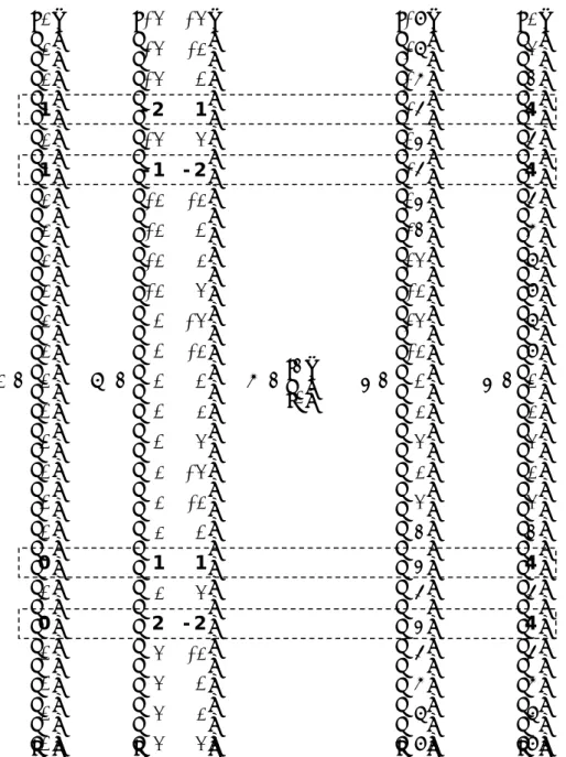
For the resolution n3, this combinatorial method is demonstrated step-by-step in the following, while the full factorial design matrix and the used vectors are shown in Fig. 3.3.1.
1) All combinations of -1, 0, 1 in 3 positions are given by the full factorial design matrix M of 33 rows by 3 columns obtained with the MATLAB command fullfact([3 3 3])–2.
2) The column-vector K = [4; 2; 1], so that the product of M and K is the column-vector F of length 33 comprising the numbers from 1 – 23 through 23 – 1.
3) The positive numbers of the vector F are transferred to the vector B as zeros, while the negative numbers are transferred as ones.
4) At the same time the negative numbers in F are completed to the positive by adding 23, so that the completed vector F’ contains the numbers from 0 through 23 – 1.
5) Since F’ contains 33 elements, any of m = 1, …, 23 – 1 appears in F’ more than once, and search for certain m results in several row indexes. The same rows of B and M compose the EXB codes for given Mn (n = 1…3). Such a gathering is demonstrated in Fig. 3.3.1, where m = 3
that corresponds to M3 = 3/8.
Comparing the obtained codes with the codes presented in Table 3.2.1 we conclude that the combinatorial method yields the same result as the procedure spawning the EXB codes.
7 6 5 5 4 2 1 2 1 1 0 7 7 6 5 7 6 5 5 4 2 1 7 6 5 5 4 3 3 2 1 3 2 1 1 0 1 -1 -2 -3 -1 -2 -3 -3 -4 -5 -5 -6 -7 -1 2 4 1 0 1 -1 0 0 1 -0 1 -1 0 1 -1 0 1 -1 0 1 -1 0 0 1 -1 1 1 0 0 1 -1 -1 1 0 0 0 1 -1 -1 -1 1 1 0 0 1 -1 -1 1 1 1 1 1 1 0 0 0 0 0 0 0 0 1 -1 -1 -1 -1 -1 -1 -0 0 0 0 0 0 0 0 0 0 0 1 1 1 1 1 1 1 1 1 1 1 3 3 3 3 3 1 -1 1 1 -1 0 1 -1 0 1 -1 1 0 1 -1 -0 0 0 1 1 F' F K M B
3.4 Translating the EXB codes to SCC topologies
For certain EXB fraction Mn, we consider a step-down SCC system that includes a
voltage source Vin, a set of n flying capacitors Cj and an output capacitor Co connected in parallel
with the load Ro. These components are connected in accordance with the EXB codes of Mn in
such a way that Co is continuously charged. In particular, the EXB coefficient A0 is responsible
for the connection of Vin, while the connection of each flying capacitor Cj is determined by the
EXB coefficient Aj. Irrespective of the connection of Vin the flying capacitors Cj are always
connected serially. To configure the EXB based SCC topologies we use the following rules: 1) If A0 = 1, then Vin is connected.
2) If A0 = 0, then Vin is not connected.
3) If Aj = -1, then Cj is charged.
4) If Aj = 0, then Cj is not connected.
5) If Aj = 1, then Cj is discharged.
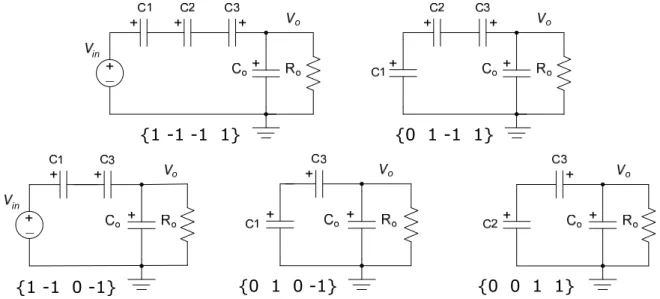
As an example we translate all the EXB codes of M3 = 3/8 presented in Table 3.4.1 to the
corresponding SCC topologies. Since the resolution n = 3 we need three flying capacitors C1, C2
and C3, the serial connection of which is determined by A1, A2 and A3 respectively. Thus, each
EXB code of M3 = 3/8 leads to a specific SCC topology as depicted in Figure 3.4.1.
Table 3.4.1.
Figure 3.4.1: SCC topologies configured from the EXB codes of M3 = 3/8.
M3 = 3/8 A0 A1 A2 A3 1 -1 -1 1 0 1 -1 1 1 -1 0 -1 0 1 0 -1 0 0 1 1 {1 -1 -1 1} {0 1 -1 1} {1 -1 0 -1} {0 1 0 -1} {0 0 1 1}
We assume that in each SCC topology of Fig. 3.4.1, the flying capacitors C1, C2 and C3
keep the voltages V1 = 2-1·Vin, V2 = 2-2·Vin and V3 = 2-3·Vin respectively. Multiplying Vin and these
voltages by the corresponding coefficients A0, A1, A2 and A3 in the EXB codes of M3 = 3/8, we
find their algebraic sum, which is equal to the target voltage Vo = 3/8·Vin.
Generally, translating all the EXB codes of certain Mn to the SCC topologies, we ought to
obtain the target voltage Vo = Mn·Vin, under the condition that each flying capacitor Cj keeps the
voltage Vj = 2-j·Vin. In the following we show that all the voltages in the EXB based SCC are
self-adjusting to the above specified values and this property is due to Corollaries 1 and 2 of the procedure for spawning the EXB codes.
3.5 Self-adjusting voltages in the EXB based SCC
“Make everything as simple as possible, but not simpler.” Albert Einstein
In this section we consider the EXB based SCC under the assumption that in each SCC topology all the capacitors voltages remain constant but of unknown values. Applying Kirchhoff’s Voltage Law (KVL) to w different SCC topologies we compose a system of w linear equations. If this system has a unique solution, we obtain the target and binary weighted voltages across the output and flying capacitors respectively.
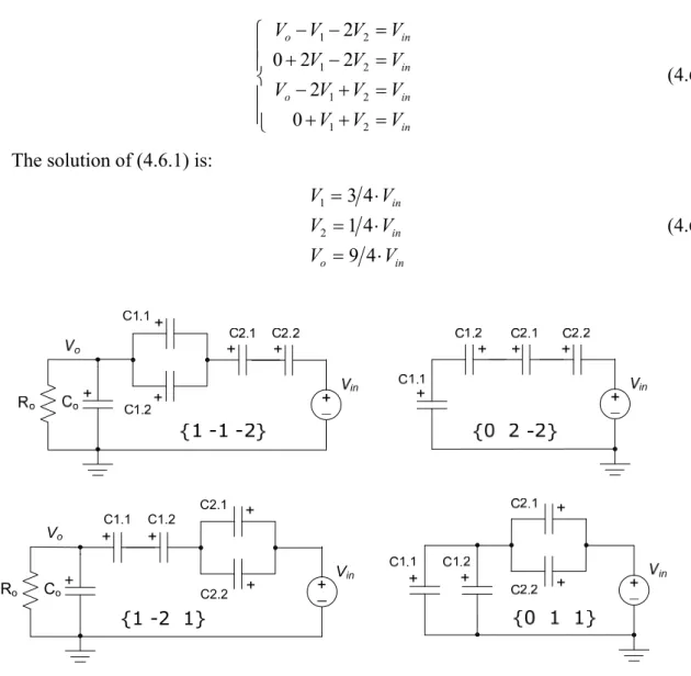
The KVL states that the algebraic sum of all voltages around any closed path in a circuit is zero. Any SCC topology is a closed path circuit because the flying capacitors are charged and discharged thus providing charge transfer. The output voltage of the SCC is assumed to be constant and the KVL is applied to the voltages across the capacitors engaged in a SCC topology. First we consider the simplest voltage halving SCC defined by M1 = 1/2. The topologies
of this SCC are depicted in Fig. 3.5.1, where C1 and Co keep the voltages V1 and Vo respectively.
Figure 3.5.1: Topologies of the voltage halving SCC. The system of linear equations for both topologies of Fig. 3.5.1 is:
o o in V V V V V 1 1 (3.5.1)
The solution of (3.5.1) is trivial: Vo V Vin
2 1 1
(3.5.2)
Generally, a system of equations for the EXB based SCC may be composed directly from the corresponding EXB codes. As an example, we show that the EXB codes of M3 = 3/8 lead not
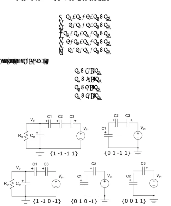
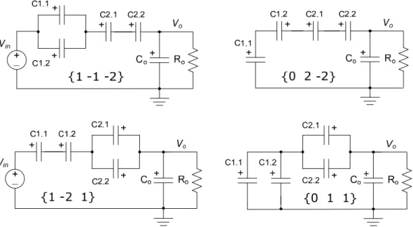
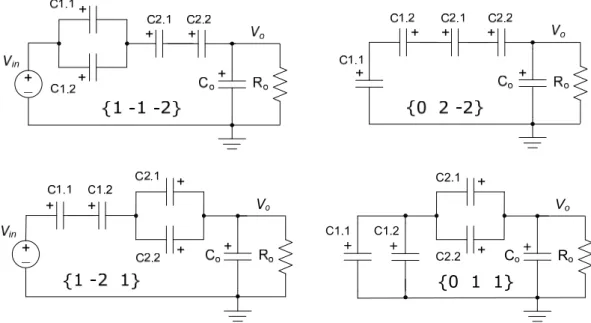
only to the SCC topologies of Fig. 3.5.2, but also to the system (3.5.3). {0 1}
Figure 3.5.2: SCC topologies configured from the EXB codes of M3 = 3/8.
o o o in o o in V V V V V V V V V V V V V V V V V V V 3 2 3 1 3 1 3 2 1 3 2 1 0 0 0 0 0 0 (3.5.3)
The number of equations in (3.5.3) is identical to the number w of all the EXB codes of M3 = 3/8 and equals to 5, while the number of unknowns is equal to 4 and defined as the
resolution n = 3 plus one. Grouping the unknowns in (3.5.3) at the left hand side yields:
0 0 0 0 0 0 3 2 3 1 3 1 3 2 1 3 2 1 o o in o o in o V V V V V V V V V V V V V V V V V V V (3.5.4)
The system of equations (3.5.4) contains two non-zero free terms as the negative value of
Vin. Generally, the connection of Vin is provided by Corollary 1 of the procedure spawning the EXB codes as follows. Consider the conventional binary code of Mn, where the coefficient Aj takes either “1” or “0”. Due to Corollary 1, the case Aj = 0 is turned to Aj = 1, which is used to generate the coefficient A0 = 1 responsible for the connection of Vin.
{1 -1 -1 1} {0 1 -1 1}
Returning to (3.5.4) we normalize it to Vin: 0 1 1 1 0 0 1 1 0 1 1 1 1 0 1 0 1 1 1 1 1 1 1 1 1 4 3 2 1 4 3 2 1 4 3 2 1 4 3 2 1 4 3 2 1 x x x x x x x x x x x x x x x x x x x x (3.5.5) where in o in in in V V x V V x V V x V V x 4 3 3 2 2 1 1 (3.5.6)
The conventional brief notation for (3.5.5) is Ax = b, where
1 1 1 0 1 1 -0 1 1 1 -0 1 -1 1 1 -1 1 1 1 -1 A 4 3 2 1 x x x x x 0 0 1 -0 1 -b (3.5.7)
In order to investigate the solvability of (3.5.5) we supplement the coefficient matrix A with the vector b and form thereby the augmented matrix A1:
0 1 1 1 0 0 1 1 -0 1 1 -1 1 -0 1 -0 1 1 1 -1 1 -1 1 1 -1 A1 (3.5.8)
According to the Kronecker-Capelli theorem [31], [36], a non-homogeneous system has at least one solution if and only if the rank of its coefficient matrix A is equal to the rank of its augmented matrix A1. This theorem has a corollary that specifies the number of solutions.
The solution is unique if and only if the rank the augmented matrix A1 equals the number of unknowns. If the rank of A equals the rank of A1, but is less than the number of unknowns, the system has an infinite number of solutions. If, on the other hand, the rank of A1 is greater than the rank of A, the system has no solutions.