HAL Id: tel-01308275
https://tel.archives-ouvertes.fr/tel-01308275
Submitted on 27 Apr 2016
HAL is a multi-disciplinary open access
archive for the deposit and dissemination of
sci-entific research documents, whether they are
pub-lished or not. The documents may come from
teaching and research institutions in France or
abroad, or from public or private research centers.
L’archive ouverte pluridisciplinaire HAL, est
destinée au dépôt et à la diffusion de documents
scientifiques de niveau recherche, publiés ou non,
émanant des établissements d’enseignement et de
recherche français ou étrangers, des laboratoires
publics ou privés.
millimeter-wave frequencies
Luca Di Palma
To cite this version:
Luca Di Palma. Reconfigurable transmitarray antennas at millimeter-wave frequencies. Signal and
Image processing. Université Rennes 1, 2015. English. �NNT : 2015REN1S092�. �tel-01308275�
ANNÉE 2015
THÈSE / UNIVERSITÉ DE RENNES 1
sous le sceau de l'Université Européenne de Bretagne
pour le grade de
DOCTEUR DE L'UNIVERSITÉ DE RENNES 1
Mention : Traitement du Signal et Télécomumnications
Ecole doctorale MATISSE
présentée par
Luca Di Palma
préparée au CEA-Leti en collaboration avec l'unité de
recherche UMR CNRS 6164
Institut d'Electronique et de Télécommunications de Rennes
UFR Informatique - Électronique
Antennes Réseaux
Transmetteurs
Recon gurables
aux Fréquences
Millimétriques
Thèse soutenue à Grenoble
le 16 décembre 2015
devant le jury composé de :
Stefano MACI
Professeur, Université de Sienne, Italie/président du jury
José A. ENCINAR
Professeur, Université de Madrid, Espagne / rapporteur
Claire MIGLIACCIO
Professeur, Université de Nice / rapporteur
Cyril MANGENOT
Chef de division, ESA-ESTEC / examinateur
Laurent PETIT
Ingénieur de recherche, Radiall / examinateur
Philippe POULIGUEN
Ingénieur de recherche, DGA-MI / examinateur
Laurent DUSSOPT
Ingénieur de recherche, CEA-Leti / encadrant
Ronan SAULEAU
“There are two possible outcomes: if the result confirms the hypothesis, then you’ve made a measurement. If the result is contrary to the hypothesis, then you’ve made a discovery.”
Contents
Acknowledgements 11
List of Figures 13
List of Tables 29
R´esum´e en franc¸ais 31
General introduction 35
1 Introduction 37
1.1 Transmitarray: operating principle . . . 37
1.2 Passive transmitarrays: State-of-the-art . . . 39
1.3 Reconfigurable transmitarrays: State-of-the-art . . . 45
1.3.1 Semiconductor varactor diodes . . . 45
1.3.2 Ferroelectric varactor diodes . . . 51
1.3.3 Microfluidics . . . 52 1.3.4 MMIC . . . 54 1.3.5 MEMS switches . . . 55 1.3.6 P-i-n diodes . . . 58 1.4 Applications . . . 60 1.4.1 Satellites communications . . . 60 1.4.2 5G heterogeneous networks . . . 64
1.4.3 Fixed radio links . . . 66
1.4.4 Radar systems . . . 68
1.5 Conclusions . . . 69
2 Circularly-polarized transmitarrays with sequential rotations 71 2.1 Sequential rotations . . . 71
2.2 Transmitarray model . . . 75
2.2.1 Focal source . . . 76 7
2.2.2 Unit-cell . . . 78
2.2.3 Model of the full transmitarray . . . 78
2.2.4 Power budget . . . 81
2.3 Passive unit-cell design . . . 82
2.4 Simulation of transmitarrays with several sequential rotation schemes . . . . 87
2.5 Mutual Coupling . . . 92
2.6 Experimental results . . . 94
2.7 Conclusions . . . 105
3 Reconfigurable unit-cell in Ka-band 107 3.1 P-i-n diode characterization . . . 107
3.2 Unit-cell design . . . 110 3.2.1 Bias network . . . 110 3.2.2 Numerical results . . . 113 3.2.3 Oblique incidence . . . 117 3.2.4 Sensitivity analysis . . . 119 3.3 Characterization setup . . . 121 3.4 Measurements . . . 127 3.5 Bias lines . . . 128
3.6 Rotation of the transmitting patch . . . 132
3.7 Conclusions . . . 134
4 Reconfigurable transmitarrays in Ka-band 137 4.1 Transmitarray in linear polarization . . . 137
4.2 Transmitarray in circular polarization . . . 139
4.2.1 Random sequential rotations . . . 150
4.2.2 Cross polarization reduction . . . 152
4.3 Prototype architecture . . . 156
4.4 Experimental results . . . 161
4.5 Conclusions . . . 174
5 Reconfigurable circularly-polarized unit-cell in Ka-band 175 5.1 Unit-cell design . . . 175 5.1.1 Bias network . . . 176 5.1.2 Numerical results . . . 178 5.1.3 Oblique incidence . . . 181 5.1.4 Sensitivity analysis . . . 183 5.2 Alternative solutions . . . 189 5.3 Characterization setup . . . 192
CONTENTS 9
5.3.1 Calibration procedure . . . 193
5.3.2 Measurement procedure . . . 194
5.4 Conclusions . . . 195
6 Radiation pattern synthesis for monopulse radar 197 6.1 Radar techniques . . . 197
6.1.1 Sequential lobing . . . 198
6.1.2 Monopulse . . . 198
6.2 Reconfigurable transmitarray in X-band . . . 202
6.3 Single-source configuration . . . 204
6.4 Four-sources configuration . . . 208
6.5 Conclusions . . . 215
General conclusions 217 A Scattering parameters in circular polarization 219 B Control boards architecture 223 C Reconfigurable transmitarray in Ka-band with planar focal sources 225 C.1 2 × 2 SIW slot array . . . 225
C.2 4 × 4 SIW slot array . . . 228
C.3 Reconfigurable transmitarray with 4 × 4 SIW slot focal array . . . 230
D Circularly-polarized unit-cell characterization setup 233 D.1 Numerical validation . . . 237
Bibliography 241
Acknowledgements
First, I would like to express my special appreciation and thanks to my supervisors Prof. Ronan Sauleau, Professor at the University of Rennes 1, and Dr. Laurent Dussopt, Senior Research Engineer at CEA-Leti. You have been great mentors during the last years. I would like to thank you for encouraging my research and for allowing me to grow as a research scientist. Your knowledge and your wisdom have been sources of inspiration.
Je suis honor´e d’avoir eu l’occasion de travailler avec vous pendant ces trois ann´ees.
I would like to express my gratitude to Dr. Patrick Potier and Dr. Philippe Pouliguen, Research Engineers at the Diretion G´en´erale de l’Armement, for having accepted to supervise
my work. The brilliant comments and suggestions you gave me during our meetings have been precious.
I would like to extend my thanks to Dr. Antonio Clemente, Research Engineer at CEA-Leti. His moral and technical support has been fundamental. I will never forget your help and our friendship. Antonio, grazie di tutto!
I would like to give thanks to Prof. Claire Migliaccio, Professor at the University of Nice Sophia-Antipolis, and Prof. Jos´e A. Encinar, Professor at the Polytechnic University of Madrid (Spain), for having accepted to evaluate this thesis manuscript and to be part of the jury. Their valuable comments have been very useful.
I extend my thanks to Prof. Stefano Maci, Professor at the University of Siena (Italy), for having accepted to participate to the defence and chairing the jury.
I express my gratitude to Dr. Cyril Mangenot, Head of Electromagnetic and Space En-vironment Division at the European Space Agency (ESA-ESTEC, Noordwijk, The Nether-lands) for the interest he demonstrated in my research activity and for having accepted to take part to the defence. I would also give thanks to Dr. Laurent Petit, Research Engineer at Radiall, for having accepted to be a member of the jury.
I would like to thank Dr. Roland Blanpain, Head of the System and Integration Depart-ment, and Dr. Dominique Noguet, Head of the Telecommunication and Security Service,
for welcoming me at the Laboratories of CEA-Leti in Grenoble. I extend my thanks to Dr. Christophe Delaveaud, Head of the Laboratory of Antennas and Propagation, for wel-coming me in his team and having supported my work. I want to mention the engineers and all the colleagues of the Laboratory. In particular, I would like to thank Raffaele, Julien, Francesco M., Jean-Fran¸cois, Francesco G., Anna, Lotfi and Laurent. Their interest in my research activity allowed to improve the quality of this work.
I would like to express my gratitude to Francesco S. and Andrea C., supportive friends and colleagues since we were first-year students in Rome. Despite the thousands of kilometres of distance, you played important roles during these years helping me throughout all the difficulties.
Finally, I would like to give special thanks to my brother, Andrea, to my parents, Stella and Marco, and to all my family. Words can not express how grateful I am to you. You have always supported me and encouraged me to follow my dreams.
Grenoble, December 2015
List of Figures
1 Sch´ema du principe de fonctionnement des r´eseaux transmetteurs. Vue 3D, en coupe et section d’une cellule ´el´ementaire. . . 32 2 Param`etres S (a) et sch´ema (b,c) de la cellule ´el´ementaire reconfigurable
de-velopp´ee en polarisation circulaire en bande Ka. (b) Cˆot´e r´eception et (c) cˆot´e transmission. Insert: photographie du syst`eme utilis´e pour la characterisation en guide d’onde. . . 33 3 Photographie du prototype r´ealis´e (a) et diagrammes de rayonnement (b)
mesur´es en chambre an´echo¨ıque `a 29 GHz pour angles de d´epointages entre -60◦ et +60◦sur le plan horizontal. . . 34 1.1 Scheme of the working principle of a transmitarray. . . 38 1.2 Scheme of the working principle of phased array (a) and reflectarray (b)
an-tennas. . . 39 1.3 Scheme of unit cell with two ground planes and a delay line. 5 × 5 array
designed and measured radiation pattern at 12 GHz [16]. . . 40 1.4 3D sketch and top view of the unit cell proposed with different angles of
rotation. Prototype of the transmitarray with 2-bit unit cells and radiation pattern at 10 GHz [18]. . . 41 1.5 Scheme of the transmitarray and different unit-cells studied in [20], [21] based
on multi-ring resonators. Simulated and measured radiation patterns at 30 GHz for a four-layer structure based on a concentric double-ring unit cell in E-plane and H-plane. . . 42 1.6 Unit-cell based on dielectric resonator. Simulated radiation patterns in the
planes φ = 0◦and φ = 90◦ at 5.8 GHz of the transmit-array [22]. . . 43 1.7 Unit-cell based on iris in waveguide. Simulated S-parameters in magnitude
and phase for all the four unit-cells proposed. Radiation patterns simulated for different offset horn configurations [23]. . . 44
1.8 3D topology and equivalent circuit model of the N th-order SEF only capac-itive layers. Simulated magnitude and phase of the transmission coefficient. Sketch of a planar lens based on the Nth-order SEF [24], [25]. . . 44 1.9 Section and top view of the reconfigurable active unit cell designed with
var-actor diodes [27]. . . 45 1.10 Realized 6 × 6 transmit-array and measured radiation pattern [28]. . . 46 1.11 Scheme of the array based on microwave phase shifters connecting 2 × 2
sub-arrays; radiation pattern for a broadside beam and beam tilted at 10◦ [29]. . 47 1.12 Photograph of the M-A-F-A prototype measured in waveguide. Simulated
and measured S-parameters in magnitude and phase [30]. . . 48 1.13 Scheme of the single unit cell and picture of the internal layer of the realized
array [31], [32]. . . 49 1.14 Measured S-parameter of the single unit cell prototype with T-bridged phase
shifter and stacked patch [31], [32]. . . 49 1.15 Measured radiation patterns on the two cardinal planes (a, b) with tilted
beams and 2D maps of synthesized shaped beams: two beams (c), three beams (d), fan (e) and a donut (f). . . 50 1.16 Unit-cell based on varactor diodes which include an amplifier. Photograph of
the realized prototype and measured scattering parameters with (a) and w/o (b) the amplifier [33]. . . 51 1.17 Transmitarray based on ferroelectric varactor diodes. Realized prototype,
unit-cell frequency response with 0V and 120V of bias voltage and measured radiation patterns [34]. . . 52 1.18 Reconfigurable unit-cell based on microfluidic split-ring resonators [35]. . . . 53 1.19 Measured scattering parameters of the unit-cell based on microfluidic
split-ring resonators in waveguide [35]. . . 53 1.20 Photograph and layer stackup of the active transmitarray submodule.
Simu-lated and measured radiation patterns at 20 GHz and 30 GHz [36]. . . 54 1.21 3D sketch of the A-F-A array, scheme and model of the coupling resonators
presented in [37]. Measured radiated pattern in the H-plane for the two arrays designed at 16 GHz and 32 GHz for several scanning angles. . . 56 1.22 Scheme and picture of the unit-cell with stripline resonator and integrated
MEMS switches. Measured unit-cell scattering parameters. Measured radia-tion patterns on E- and H-planes [38]. . . 57 1.23 3D sketch of the MEMS devices produced by CEA-LETI and used in the
transmitarray unit-cell implementation. Measured scattering parameters in waveguide setup [39]. . . 57
LIST OF FIGURES 15 1.24 Side view, top view and bottom view of the reconfigurable 1-bit unit cell
based on p-i-n diodes [40]. . . 58 1.25 Simulated and measured S-parameters (magnitudes) in the two phase states
in waveguide WR90. Simulated and measured phase difference [40]. . . 59 1.26 Measured gain of the transmit-array for the different phase distribution in
H-plane [40]. . . 59 1.27 Unit-cell based on 4 p-i-n diodes with 1 bit of phase quantization and linear
polarization control. Measured scattering parameters in waveguide [41]. . . . 60 1.28 Coverage of the Eutelsat satellite KA-SAT in the ITU region 1 [42]. . . 60 1.29 Satellite channels in Ku- and Ka-band for the ITU region 1 [43]. . . 61 1.30 Radiation masks provided by ITU S.465-6, S.580-6 [46] and provided by FCC
[47] 25.209 for the earth station. . . 62 1.31 Radiation masks provided by FCC 25.138 [48] for the earth station and by
ETSI EN 303 978 [47] for the earth stations on mobile platforms (ESOMPs). 63 1.32 Sketch of a heterogeneous wireless network with backhauling channels. . . 64 1.33 Rain attenuation in dB/km across frequency at various rainfall rates. The
rain attenuation at 28 GHz has an attenuation of 7 dB/km for a very heavy rainfall of 25 mm/hr. Attenuation caused by atmospheric absorption. It is 0.012 dB over 200 m at 28 GHz and 0.016 dB over 200 m at 38 GHz. . . 65 1.34 Experimental setup and measured path losses at 28 GHz in the experiment
carried out at the NYU, US [53]. . . 65 1.35 Experimental setup and measured path losses at 37.6 GHz in the experiment
carried out at the University of Texas, US [53]. . . 66 1.36 Radiation masks provided by ETSI EN 302 217-4-2 [47] for the point-to-point
links in the 24-30 GHz band. Antenna classes 2, 3 and 4 are reported. . . 67 1.37 Radiation masks provided by ETSI EN 302 217-4-2 [47] for the point-to-point
links in the 30-47 GHz band. Antenna classes 2, 3A and 4 are reported. . . . 67
2.1 Scheme of a phased four-elements sub-array with sequental rotations (T =4,
p=2) (a) and example of a feeding network based on quarter-wavelength
impedance transformers and delay lines in microstrip technology (b) [58]. . . 72 2.2 Scheme of the setup considered in a first-order analysis for T =4. . . . 73 2.3 Simulated co-polar radiation pattern of the three horn antennas (Flann
22240-10 (WR-28), ATM 28-440-6 (WR-28) and ATM 34-440-6 (WR-34)) compared with the cosine function. . . 76 2.4 Simulated and measured co-polar radiation pattern of a WR34 standard gain
2.5 Measured co-polar (a) and cross-polar (b) radiation patterns of a WR34 stan-dard gain horn with 10 dBi of nominal gain in the horizontal plane. . . 77 2.6 Schematic view of the setup used for the calculation of the unit-cell scattering
parameters (a) and (b) radiation patterns. . . 78 2.7 Scheme of the model used for the analysis of transmitarray antennas. . . 79 2.8 Schematic view of the power budget quantities considered in the proposed
transmitarray model. . . 81 2.9 Scheme of the circularly-polarized unit-cell. Receiving and transmitting
lay-ers. All the dimensions are listed in Table 2.3. . . 83 2.10 Full-wave simulation setup used to calculate the radiation patterns for the
transmitting layer (ψc= 0◦). A similar configuration has been considered for
the receiving layer side. . . 84 2.11 Scattering parameters magnitudes of the unit-cell simulated with periodic
boundary conditions and Floquet port excitations (ψl= ψc= 0◦). A similar
behavior is obtained for the different values of ψc. . . 84
2.12 Radiation pattern at 29.4, 30 and 30.4 GHz (a), broadside realized gains and axial ratio (b) of the unit-cell from transmitting circularly-polarized side. . . 85 2.13 Radiation pattern at 28, 30 and 31 GHz (a) and broadside realized gains (b)
of the unit-cell from receiving linearly-polarized side. . . 86 2.14 Broadside gain and efficiency of the 400-elements transmitarray without
ro-tations at 30.0 GHz as a function of the focal distance F . . . . 87 2.15 Axial ratios in the broadside direction for the transmitarray without and with
sequential rotation schemes of Fig. 2.16(f),(g),(h). . . 88 2.16 Scheme of sequential rotations applied to the transmitting layer of the
trans-mitarray: without rotations (a); with rotations of 0◦/90◦ (b) in a chessboard arrangement; with rotations of 0◦/60◦/120◦ (c), 0◦/120◦/240◦ (d) in a diag-onal arrangement; with rotations of 0◦/45◦/90◦/135◦ (e), 0◦/90◦/180◦/270◦ (f) in a clockwise arrangement; with rotations of 0◦/90◦/180◦/270◦ in two different rotated sub-array arrangements (g, h). The corresponding receiv-ing layers are formed by different arrangements of linearly-polarized patch antennas rotated by ψl= 0◦,180◦ accordingly with Eqns. 2.13, 2.14. . . 89
2.17 Phase distributions applied to the transmitarray surface with the different schemes of rotations (w/o rotations (a), clockwise (b), 4-element sub-array (c, d) rotations). These schemes correspond to the rotation configurations (a), (f), (g) and (h) of Fig. 2.16, respectively. . . 91 2.18 Radiation pattern in the horizontal plane w/o rotations and with rotation
LIST OF FIGURES 17 2.19 Simulation setup considered for the calculation of the embedded pattern of a
transmitarray without (a) and with (b) sequential rotations. . . 93 2.20 Full-wave simulation setup (top view of the transmitting layer) considered for
the calculations of the embedded pattern of thetransmitarray with sequential rotations: ψc = 0◦ (a), ψc = 90◦ (b), ψc = 180◦ (c), ψc = 270◦ (d). The
patch antenna drawn in red is the excited one; all the others are closed to a matched load. . . 94 2.21 Embedded pattern of the single unit-cell calculated at 30.0 GHz with the
setup shown in Fig. 2.19; Co-polar (a) and cross-polar (b) magnitudes, co-polar phases (c). . . 95 2.22 Co- and cross-polarized broadside CP gains for the transmitarray without
rotations (A; Fig. 2.16a) and for the transmitarray with sequential rotations (B; Fig. 2.16h). The unit cell embedded patterns have been calculated with the two setups of Fig. 2.19 for the two transmitarrays, respectively. . . 96 2.23 Photograph of the measurement setup in anechoic chamber (a). Photographs
of the realized prototype (receiving and transmitting layer) (b) and micro-scope images of the single unit-cell on the array surface (c). . . 97 2.24 Broadside axial ratio for the transmitarray without rotations (A; Fig. 2.16a)
and for the transmitarray with sequential rotations (B; Fig. 2.16h). The unit cell embedded patterns have been calculated with the two setups of Fig. 2.19 for the two transmitarrays, respectively. . . 98 2.25 Simulated and measured axial ratio for the transmitarray with rotations (B;
Fig. 2.16h) in the main beam region (15◦,15◦) at 28, 30 and 32 GHz. . . 98 2.26 Simulated and measured radiation patterns (co-polar and cross-polar
compo-nents in circular polarization) in the horizontal plane at 30 GHz. . . 100 2.27 Simulated and measured radiation patterns (co-polar and cross-polar
compo-nents in circular polarization) in the diagonal plane at 30 GHz. . . 101 2.28 Simulated and measured radiation patterns (co-polar and cross-polar
compo-nents in circular polarization) in the horizontal plane at 29 GHz. . . 102 2.29 Simulated and measured radiation patterns (co-polar and cross-polar
compo-nents in circular polarization) in the horizontal plane at 31 GHz. . . 103 2.30 Simulated and measured radiation patterns (co-polar and cross-polar
compo-nents in circular polarization) in the horizontal plane at 32 GHz. . . 104
3.1 Scheme and geometrical dimensions (in millimetres) of the p-i-n diode Flip-chip packaging MA4AGP907 manufactured by M/ACOM technologies [83]. . 108
3.2 Photograph of the setup used for the characterization of the p-i-n diode. It includes: a diode mounted on a coplanar line, two microwave probes (GSG configuration with 350 µm of pitch), a VNA and a DC power supply. . . 108 3.3 Simulated and measured scattering parameters (magnitudes (a, c) and phases
(b, d)) of the p-i-n diode in the reverse (a, b) and forward (c, d) states. . . . 109 3.4 Equivalent circuit model for a p-i-n diode in the reverse (a) and forward (b)
states. RON = 4.2 Ω, LON = 0.05 nH, ROF F = 300 kΩ, COF F = 42 fF. . . . 109
3.5 Scheme of the unit-cell architecture. Exploded view (a), receiving layer (b), biasing layer (c) and transmitting layer (d). Details of the model used for the diodes in the full wave simulations are given in the circular inset. . . 111 3.6 Scattering parameters simulated for the RF/DC decoupling circuit formed
by a distributed capacitor of area 2.5 × 0.5 mm2. Inset: 3D sketch of the
simulation setup. . . 112 3.7 Scattering parameters (magnitude (a) and phases (b)) of the unit-cell
simu-lated with periodic boundary conditions and Floquet port excitation. . . 114 3.8 3D sketch of the simulation setup used for the radiation pattern calculation.
A Floquet port is placed in front of the active patch antenna side. A radiation boundary is placed in front of the active patch side. For the calculation of the radiation pattern from the opposite side these two conditions are inverted. 115 3.9 Broadside realized gain (a) and radiation pattern at 28.0, 29.0 and 30.0 GHz
(b) in the H-plane of the unit-cell active layer. A Floquet port is placed in front of the passive patch antenna side. A radiation boundary is placed in front of the active patch side. . . 116 3.10 Broadside realized gain (a) and radiation pattern at 28.0, 29.0 and 30.0 GHz
(b) in the H-plane of the unit-cell passive layer. A Floquet port is placed in front of the active patch antenna side. A radiation boundary is placed in front of the passive patch side. . . 116 3.11 Scattering parameters simulated with different incidence angles in the
E-plane: S11 (a), S21 (b), S22 (c). . . 118
3.12 Scattering parameters simulated with different incidence angles in the H-plane: S11 (a), S21 (b), S22 (c). . . 119
3.13 Simulated scattering parameters magnitudes (S11(a), S21(b), S22(c)) of the
unit-cell for different values of L1, L2 and L3. . . 121
3.14 Full-wave simulation setup of the unit-cell in waveguide. . . 121 3.15 Simulated and measured scattering parameters magnitudes (0◦state) in
LIST OF FIGURES 19 3.16 Simulated and measured scattering parameters magnitudes (180◦ state) in
WR-28 waveguide: S11, S21 (a) and S22 (b). Simulated and measured phase
difference between the two states (c). . . 124 3.17 Photograph of the unit-cell prototype (receiving (a) and transmitting (b)
layers) and cut-view on the horizontal axis of the structure. Dimensions are given in millimeters. . . 125 3.18 Photograph of the full measurement setup in standard waveguide WR-28 used
for the characterization. . . 126 3.19 Scheme of the waveguide setup used to test the unit-cell. Dimensions are
given in millimeters. . . 126 3.20 Unit-cell with ten bias lines accommodated in the transmitting (a) and biasing
(b) layers. Scattering parameters magnitudes for the single unit-cell without and with ten bias lines (c). . . 128 3.21 Simulation setup used to evaluate the effects of the bias lines on the unit-cell
frequency response: 3D sketch (a) and transmitting (b). Scattering param-eters magnitudes for three unit-cells with bias lines compared to the single unit-cell (c). . . 129 3.22 Schemes of the unit-cell with ten bias lines connected to the center (a, b) or
to the side (c, d) tested in waveguide. . . 129 3.23 Measured scattering parameters magnitudes (a, b) and phases (c) of the single
unit-cell in waveguide with ten bias lines and a center bias signal connection. 130 3.24 Measured scattering parameters magnitudes (a, b) and phases (c) of the single
unit-cell in waveguide with ten bias lines and a side bias signal connection. . 131 3.25 Photographs of the tested unit-cell prototypes with integrated bias lines:
cen-ter (a, c) and side (b, d) connections. . . 132 3.26 Measured scattering parameters magnitudes (a, b) and phases (c) of the single
unit-cell in waveguide with ten bias lines and passive patch rotated by 90◦. . 133 3.27 Scheme of the waveguide setup used to test the unit-cell with 90◦rotated patch.134 3.28 Photographs of the tested unit-cell prototypes with integrated bias lines and
a 90◦ rotation of the passive patch: active (a) and passive (b, d) patch layers. 134 4.1 Simulated broadside gain and directivity of a 400-elements transmitarray
based on the unit-cell of Chapter 3 and working in linear polarization. . . 138 4.2 Radiation patterns in the φ = 90◦ plane at 29.0 GHz for the co-polar linear
polarization of a 400-elements transmitarray formed by the unit-cell design proposed in Chapter 3. Main beam at broadside and at -30◦ with the corre-sponding phase distribution. . . 138 4.3 Frequency response for the broadside beam configuration shown in Fig. 4.2. . 138
4.4 Radiation patterns in the φ = 90◦ plane for the co-polar linear polarization at 27.4, 29.0 and 31.0 GHz of a 400-elements transmitarray formed by the unit-cell design proposed in Chapter 3. . . 139 4.5 Sequential rotations schemes considered in the transmitting layer: 4 × 4
sub-array (a) and clockwise (b) arrangements. . . 140 4.6 Layouts of the receiving and transmitting layers corresponding to the schemes
of Fig. 4.5: 4 × 4 sub-array (a) and clockwise (b) arrangements. . . 141 4.7 Simulated radiation patterns (realized gains in circular polarization) in the
φ = 90◦ plane (a) and 2D maps (b,c) with the main beam at broadside and the rotation scheme shown in Fig.4.5(a). The calculated optimal phase distribution on the transmitting layer at 29.0 GHz is shown in the inset. . . . 142 4.8 Phase distributions calculated for the clockwise rotation scheme (Fig. 4.5(a))
with 0◦ (a, b), -20◦ (c, d) and -40◦ (e, f) tilted beams in the φ=90◦ plane. Right-handed (a, c, e) and left-handed (b, d, f) circularly-polarized main beams. The receiving layer distributions, realized with the proper states of p-i-n diodes, for the configurations (a) and (b) are shown in Fig. 4.9. . . 143 4.9 Receiving layer compensation masks for the phase distributions shown in Fig
4.8(a, b). . . 144 4.10 Simulated radiation patterns (a) (realized gain) in the φ = 90◦ plane and 2D
maps (b,c) for the phase distributions (a) (solid lines) and (b) (markers) of Fig. 4.8. . . 144 4.11 Simulated radiation patterns (realized gain) in the φ = 90◦ plane (a) and 2D
maps (b,c) for the phase distributions (c) (solid lines) and (d) (markers) of Fig. 4.8. . . 144 4.12 Simulated radiation patterns (realized gain) in the φ = 90◦ plane (a) and 2D
maps (b,c) for the phase distributions (e) (solid lines) and (f) (markers) of Fig. 4.8. . . 145 4.13 Simulated radiation pattern (realized gain) in the φ = 45◦ plane with main
beam tilted at -20◦in the same azimuthal plane. Inset: optimal phase distri-bution. . . 146 4.14 Simulated radiation patterns (realized gain) in the φ = 45◦ plane with main
beam tilted at -30◦in the same azimuthal plane. Inset: optimal phase distri-bution. . . 146 4.15 Simulated radiation patterns (realized gain) in the φ = 45◦ plane with main
beam tilted at -40◦in the same azimuthal plane. Inset: optimal phase distri-bution. . . 146
LIST OF FIGURES 21 4.16 Simulated 2D radiation patterns (realized gain) with main beam tilted at -20◦
(a, b), -30◦ (c, d), -40◦ (e, f) in the φ = 45◦. Co-polar RHCP (a, c, e) and cross-polar LHCP (b, d, f) components. . . 147 4.17 Simulated radiation patterns (realized gain) in the φ = 45◦ plane with the
main beam tilted at -45◦ in the same azimuthal plane. Inset: optimal phase distribution. . . 148 4.18 Simulated 2D radiation patterns (realized gain) with the main beam tilted at
-40◦ in the φ = 20◦ plane. Co- (a) and cross-polar (b) components. . . 148 4.19 Random sequential rotation scheme applied to the transmitting layer of the
transmitarray. . . 150 4.20 Simulated radiation patterns (realized gain) in the φ = 90◦plane (a) and 2D
maps (b,c). Inset: optimal phase distribution. . . 151 4.21 Frequency response of the 400-elements transmitarray with a broadside beam
with the clockwise (markers) and random (solid lines) sequential rotation schemes of Fig. 4.5(b) and Fig. 4.19, respectively. . . 151 4.22 Simulated radiation patterns (realized gain) in the φ = 90◦ plane. Inset:
optimal phase distribution calculated with the random rotation scheme of Fig. 4.19. . . 152 4.23 Simulated radiation patterns (realized gain) with tilted beam at -20◦: φ =
90◦ plane (a) and 2D maps (b,c). Inset: optimal phase distribution. . . 152 4.24 Simulated radiation patterns (realized gain) with tilted beam at -40◦: φ =
90◦ plane (a) and 2D maps (b,c). Inset: optimal phase distribution. . . 153 4.25 Simulated radiation patterns (realized gain) in the φ = 45◦plane (a) and 2D
maps (b,c) with the main beam tilted at -20◦ in the same azimuthal plane. Inset: optimal phase distribution. . . 153 4.26 Simulated radiation patterns (realized gain) in the φ = 45◦plane (a) and 2D
maps (b,c) with the main beam tilted at -30◦ in the same azimuthal plane. Inset: optimal phase distribution. . . 154 4.27 Simulated radiation patterns (realized gain) in the φ = 45◦plane (a) and 2D
maps (b,c) with the main beam tilted at -40◦ in the same azimuthal plane. Inset: optimal phase distribution. . . 154 4.28 Simulated radiation patterns (realized gain) in the φ = 20◦ plane with the
main beam tilted at -40◦ in the same azimuthal plane. Inset: optimal phase distribution. . . 154
4.29 Simulated co-polar (black curve) and cross-polar (markers) realized gain in correspondence of the main beam tilted at -40◦ in the φ = 45◦ plane as a function of the phase offset. Maximum cross-polar gain (gray curve) in all cut-planes as a function of the phase offset. . . 155 4.30 Simulated radiation pattern (realized gain) in the φ = 45◦ plane with main
beam tilted at -40◦in the same azimuthal plane. Inset: optimal phase distri-bution with optimized phase offset (220◦). . . 155 4.31 Quarter of the final array configuration (10 × 10 unit-cells), view of the
re-ceiving layer with 50 bias lines connected to the 2 × 50 pins 1.27-mm SMT connector with 2 × 50 pins. . . 156 4.32 Quarter of the final array configuration (10 × 10 unit-cells), view of the
trans-mitting layer. . . 157 4.33 Quarter of the final array configuration (10 × 10 unit-cells), view of the biasing
layer with 50 bias lines arrangement. . . 158 4.34 Bias line arrangement on a half transmitarray row (both the receiving and
biasing layers are visible). . . 158 4.35 Scheme of the complete transmitarray prototype (receiving layer). . . 159 4.36 Scheme of the complete transmitarray prototype (transmitting layer). . . 159 4.37 Photograph of the setup used to test the control boards. . . 160 4.38 Photographs of the realized transmitarray prototype in Ka-band. . . 160 4.39 Sketch of the setup used for the characterization (a) and photographs (b) of
the realized prototype in anechoic chamber. . . 161 4.40 Simulated (solid lines) and measured (solid bold lines) realized gains in RHCP
and LHCP at broadside and measured broadside axial ratio (markers). . . 162 4.41 Simulated (solid lines) and measured (solid bold lines) radiation patterns
(realized gain) at 29.0 GHz in the vertical plane. LHCP beam at broadside (vertical plane). . . 163 4.42 Simulated (solid lines) and measured (solid bold lines) radiation patterns
(realized gain) at 29.0 GHz in the vertical plane. RHCP beam at broadside (vertical plane). . . 163 4.43 Simulated and measured axial ratio in the main beam angular region
(broad-side configuration) at 27.4, 29.0 and 31.0 GHz. . . 163 4.44 Simulated (solid lines) and measured (solid bold lines) radiation patterns
(realized gain) at 29.0 GHz in the horizontal plane. LHCP beam at -30o
LIST OF FIGURES 23 4.45 Simulated (solid lines) and measured (solid bold lines) radiation patterns
(realized gain) at 29.0 GHz in the horizontal plane. RHCP beam at -30o
(horizontal plane). . . 164 4.46 Simulated (solid lines) and measured (solid bold lines) radiation patterns
(realized gain) at 29.0 GHz in the horizontal plane. LHCP beam at 40o (hor-izontal plane). . . 164 4.47 Simulated (solid lines) and measured (solid bold lines) radiation patterns
(realized gain) at 29.0 GHz in the horizontal plane. RHCP beam at 40o (horizontal plane). . . 165 4.48 Simulated (solid lines) and measured (solid bold lines) radiation patterns
(realized gain) at 29.0 GHz in the vertical plane. LHCP beam at -30o(vertical
plane). . . 165 4.49 Simulated (solid lines) and measured (solid bold lines) radiation patterns
(realized gain) at 29.0 GHz in the vertical plane. RHCP beam at -30o(vertical
plane). . . 165 4.50 Simulated (solid lines) and measured (solid bold lines) radiation patterns
(realized gain) at 29.0 GHz in the vertical plane. LHCP beam at 40o(vertical plane). . . 166 4.51 Simulated (solid lines) and measured (solid bold lines) radiation patterns
(realized gain) at 29.0 GHz in the vertical plane. RHCP beam at 40o(vertical
plane). . . 166 4.52 Simulated (solid lines) and measured (solid bold lines) radiation patterns
(re-alized gain) at 29.0 GHz in the diagonal plane. LHCP beam at -20o(diagonal
plane). . . 166 4.53 Simulated (solid lines) and measured (solid bold lines) radiation patterns
(re-alized gain) at 29.0 GHz in the diagonal plane. RHCP beam at -20o(diagonal
plane). . . 167 4.54 Simulated and measured axial ratio in the main beam angular region (-20o
tilted beam in the diagonal plane) at 27.4, 29.0 and 31.0 GHz. . . 167 4.55 Simulated (solid lines) and measured (solid bold lines) radiation patterns
(re-alized gain) at 29.0 GHz in the diagonal plane. LHCP beam at -40o(diagonal plane). . . 167 4.56 Simulated (solid lines) and measured (solid bold lines) radiation patterns
(re-alized gain) at 29.0 GHz in the diagonal plane. RHCP beam at -40o(diagonal
plane). . . 168 4.57 Measured radiation patterns (LHCP realized gain) at 29.0 GHz in the
4.58 Measured radiation patterns (RHCP realized gain) at 29.0 GHz in the hori-zontal plane with different steering angles. . . 168 4.59 Measured radiation patterns (LHCP realized gain) at 29.0 GHz in the vertical
plane with different steering angles. . . 169 4.60 Measured radiation patterns (RHCP realized gain) at 29.0 GHz in the vertical
plane with different steering angles. . . 169 4.61 Measured radiation patterns (LHCP realized gain) at 29.0 GHz in the diagonal
plane with different steering angles. . . 169 4.62 Measured radiation patterns (RHCP realized gain) at 29.0 GHz in the
diago-nal plane with different steering angles. . . 170
5.1 Scheme of the unit-cell architecture. Exploded view (a), transmitting layer (b), biasing layer (c), receiving layer (d) and cut view (e). . . 177 5.2 Scheme of the HFSS model used to calculate the scattering parameters for
the unit-cell of Fig. 5.1. . . 178 5.3 Scattering parameters (magnitude (a) and phase (b)) of the unit-cell
simu-lated with periodic boundary conditions and Floquet port excitation. S11and
S22 are the reflection coefficients calculated from the linearly-polarized and
circularly-polarized layers, respectively. The transmission coefficients S21l,
S21r are referred to the circular polarization and they have been calculated
as reported in Appendix A. . . 179 5.4 Broadside realized gains, axial ratio (a) and radiation pattern at 28.4, 28.8
and 29.4 GHz (b) of the unit-cell simulated with periodic boundary conditions.180 5.5 Scattering parameters simulated with different incidence angles in the
E-plane: S11 (a), S21 (b) and S22 (c). . . 182
5.6 Scattering parameters simulated with different incidence angles in the H-plane: S11 (a), S21 (b) and S22 (c). . . 183
5.7 Simulated scattering parameters magnitudes (S11(a), S21(b), S22(c)) of the
unit-cell for different values of L2. . . 185
5.8 Simulated scattering parameters magnitudes (S11(a), S21(b), S22(c)) of the
unit-cell for different values of Lg2 and wg2. . . 186
5.9 Simulated scattering parameters magnitudes (S11(a), S21(b), S22(c)) of the
unit-cell for different values of L1 and t2. . . 187
5.10 Simulated scattering parameters magnitudes (S11(a), S21(b), S22(c)) of the
unit-cell for different values of dV. . . 188
5.11 Simulated broadside axial ratio of the unit-cell Fig. 5.1 for different values of
LIST OF FIGURES 25 5.12 Scheme of the four unit-cell architectures considered for generating the
circu-lar pocircu-larization in the transmitting layer. Dimensions are given in millimeters. 190 5.13 Simulated scattering parameters magnitudes (S11(a), S21(b), S22(c)) of the
different unit-cells shown in Fig. 5.12. . . 191 5.14 Scheme of the waveguide setup for the first measurement in which the
scat-tering parameters associated to the vertical polarization are measured. . . 193 5.15 Scheme of the waveguide setup for the second measurement in which the
scattering parameters associated to the horizontal polarization are measured. 193 5.16 Scheme of the waveguide setup for the third measurement in which the
scat-tering parameters associated to the transmission between the vertical and horizontal polarization are measured. . . 193
6.1 3D sketch of the sequential-lobing tracking radar principle. Only two beams for the tracking in elevation angle are considered for the sake of simplicity. . . 199 6.2 Schemes of the lobes sequentially generated in the sequential-lobing radar.
Four beams and conical scan. . . 199 6.3 3D sketch of the monopulse tracking radar principle. Only two beams for the
tracking in elevation angle are considered for the sake of simplicity. . . 200 6.4 Scheme of the receiver needed for a two-quadrant monopulse tracking radar
with amplitude comparison. . . 201 6.5 3D sketch of the reconfigurable transmitarray for monopulse radar applications.203 6.6 3D sketch of the focal source plane of the single- and multiple- source
config-urations. . . 203 6.7 Optimized phase distributions for the single-source configuration with main
beam direction at broadside (Σ(a), ∆ (b,c) patterns) and tilted at 20◦ in the horizontal plane (∆-pattern) (d). . . 204 6.8 Simulated radiation pattern in the horizontal plane at 10 GHz with Σ and ∆
patterns generated with the two proposed transmitarray configurations. . . . 205 6.9 Photograph of the X-band monopulse radar based on a transmitarray antenna
architecture in anechoic chamber. . . 206 6.10 Simulated and measured Σ and ∆ radiation patterns at 10 GHz for the single
source configuration with a broadside beam. . . 207 6.11 Simulated and measured Σ and ∆ radiation patterns at 10 GHz for the single
source configuration with a 20◦tilted beam. . . 207 6.12 Measured ∆ radiation patterns for the single source configuration with a
broadside beam (a) and a 20◦ tilted beam (b) as a function of the frequency. 208 6.13 Simulated realized gain as a function of the focal distance F and of the
6.14 Optimized phase distributions for the multisource configurations with a beam direction at broadside (a) and tilted by 20◦ (b) in the horizontal plane and 30◦ (c), 40◦ (d) in the vertical plane. . . 209 6.15 Photograph of the X-band monopulse radar based on a transmitarray antenna
architecture in anechoic chamber in the single and four sources configurations. 210 6.16 Simulated and measured Σ and ∆ radiation patterns at 10 GHz for the
four-sources configuration with a broadside beam. . . 211 6.17 Simulated and measured Σ and ∆ radiation patterns at 10 GHz for the
four-sources configuration with a 20◦ tilted beam. . . 211 6.18 Measured ∆ radiation patterns for the four-sources configuration with a
broad-side (a) and a 20◦ tilted (b) beam as a function of the frequency. . . 212 6.19 Scheme of the feeding network for the four-sources configuration in order to
realize a four-quadrant monopulse radar system. . . 212
A.1 Scheme of incident and emerging waves considered in the scattering parame-ters evaluation in circular polarization. . . 220
B.1 Photograph of the transmitarray prototype with the four control boards and scheme of their PCB stacking. . . 223 B.2 Scheme of the working principle of each control board. . . 224
C.1 Sketches of a waveguide in SIW technology (a) and its equivalent standard waveguide (b). . . 226 C.2 3D sketch (a) and microstrip transition detail (b) for the 2 × 2 array of slot
antenna designed in SIW technology. . . 227 C.3 Measured and simulated reflection coefficient (a) and radiation pattern in the
vertical plane (E-plane) at 29 GHz (b) for the 2 × 2 array of slot antennas designed in SIW technology. . . 227 C.4 Measured 2D maps of the co-(a) and cross-polarized components (b) for the
2 × 2 array of slot antennas designed in SIW technology. . . 227 C.5 3D sketch (a) and photograph (b) of the 4 × 4 array of slot antenna designed
in SIW technology designed as focal source of the transmitarray antenna proposed in Chapter IV. . . 228 C.6 Measured and simulated reflection coefficient (a) and broadside gain (b) for
the 4 × 4 array of slot antennas designed in SIW technology. . . 229 C.7 Measured radiation pattern of the co- and cross-polarized components in the
horizontal (a) and vertical (b) planes at 29 GHz for the 4 × 4 array of slot antenna designed in SIW technology. . . 229
LIST OF FIGURES 27 C.8 Measured 2D maps of the co-(a) and cross-polarized components (b) for the
2 × 2 array of slot antenna designed in SIW technology. . . 229 C.9 Photograph of the transmitarray prototype of Chapter IV with the 4 × 4 array
of slot antennas as focal source. . . 230 C.10 Simulated and measured radiation patterns at 29 GHz of the co- and
cross-polarized components (normalized gain) for the transmitarray with the 4 × 4 array of slot antennas designed in SIW technology: beam at broadside. . . 231 C.11 Simulated and measured radiation patterns at 29 GHz of the co- and
cross-polarized components (normalized gain) for the transmitarray with the 4 × 4 array of slot antennas designed in SIW technology: tilted beams at -20◦ (a) and -40◦ (b) in the horizontal plane. . . 231 C.12 Simulated and measured radiation patterns of the co- (a, c, e) and cross- (b,
d, f) polarized components (normalized gain) for the transmitarray with the 4 × 4 array of slot antennas designed in SIW technology: broadside beam (a, b) and tilted beams at -20◦ (c, d) and -40◦ (e, f) in the horizontal plane. . . . 232 D.1 Scheme of waveguide setup formed by two junctions J1 and J2, considered for
the circularly-polarized unit-cell characterization. It includes two rectangular WR-28 straight waveguides, a square waveguide section, an OMT and two adaptors. . . 234 D.2 Scheme of junction 2 connected to the adaptor in WR28 (Lm=9 mm). . . 234
D.3 Scheme of the short circuit method applied to the junction 2 for the vertical polarization. . . 235 D.4 Scheme of simulated waveguide setup. It includes: a simple narrow-band
OMT formed by a square waveguide and two orthogonal rectangular WR-28 waveguides, a square waveguide (6.5 × 6.5 mm2), two waveguide adaptors, the unit-cell PCB and a rectangular WR-28 waveguide. Simulated electric-field at 29 GHz. . . 238 D.5 Simulated scattering parameters of the measurements setup in magnitude (a)
List of Tables
2.1 Angles of rotations assigned to the antenna m for different T and p values. . 75 2.2 Geometrical dimensions of the horn antennas considered as feed (Fig. 2.3). . . 77 2.3 Unit-cell geometrical dimensions. . . 83 2.4 Simulated radiation characteristics at 30 GHz of a 400-elements transmitarray
with the sequential rotation schemes of Fig. 2.16. AR and XPD calculated on a 10% fractional bandwidth. . . 90 2.5 Simulated radiation characteristics at 30 GHz of a 400-elements transmitarray
with the sequential rotation schemes of Fig. 2.16. AR and XPD calculated on a 10% fractional bandwidth. . . 90 2.6 Power budget and radiation characteristics at 30 GHz for the realized
proto-type with sequential rotation (h) of Fig. 2.16. . . 99
3.1 Unit-cell geometrical dimensions of Fig. 3.5 in millimetres. . . 112 3.2 Simulated and measured performance in the waveguide setup. The simulation
setup of Fig. 3.14 has been considered. . . 127
4.1 Radiation characteristics of a 400-elements transmitarray working in linear polarization. . . 139 4.2 Radiation characteristics of a 400-elements transmitarray working in RHCP
circular polarization with the sequential rotation schemes of Fig 4.5. . . 149 4.3 Power budget and radiation characteristics at 29.0 GHz for the transmitarray
configurations of Fig. 4.5. . . 149 4.4 Power budget and radiation characteristics at 29.0 GHz for the realized
pro-totype at broadside. . . 170 4.5 Simulated and measured radiation characteristics of the tested reconfigurable
transmitarray at 29.0 GHz. LHCP beams in the horizontal plane. . . 171 4.6 Simulated and measured radiation characteristics of the tested reconfigurable
transmitarray at 29.0 GHz. RHCP beams in the horizontal plane. . . 171 29
4.7 Simulated and measured radiation characteristics of the tested reconfigurable transmitarray at 29.0 GHz. LHCP beams in the vertical plane. . . 172 4.8 Simulated and measured radiation characteristics of the tested reconfigurable
transmitarray at 29.0 GHz. RHCP beams in the vertical plane. . . 172 4.9 Simulated and measured radiation characteristics of the tested reconfigurable
transmitarray at 29.0 GHz. LHCP beams in the diagonal plane. . . 173 4.10 Simulated and measured radiation characteristics of the tested reconfigurable
transmitarray at 29.0 GHz. RHCP beams in the diagonal plane. . . 173 5.1 Unit-cell geometrical dimensions in millimetres. . . 176 5.2 Unit-cells simulated performance in the 0◦ state. . . 192 6.1 Focal source excitation phase for ∆-pattern generation in the four-sources
configuration. . . 211 6.2 Simulated and measured Σ-radiation pattern characteristics at 10 GHz for the
single-source configuration. . . 213 6.3 Simulated and measured ∆-radiation pattern characteristics at 10 GHz for
the single-source configuration in the E-plane. . . 213 6.4 Simulated and measured ∆-radiation pattern characteristics at 10 GHz for
the single-source configuration in the H-plane. . . 213 6.5 Simulated and measured Σ-radiation pattern characteristics at 10 GHz for the
four-sources configuration. . . 214 6.6 Simulated and measured ∆-radiation pattern characteristics at 10 GHz for
the four-sources configuration in the E-plane. . . 214 6.7 Simulated and measured ∆-radiation pattern characteristics at 10 GHz for
R´
esum´
e en fran¸
cais
De nombreuses applications civiles et militaires (faisceaux hertziens, communications par satellite, radars automobiles, syst`emes d’imagerie haute r´esolution) n´ecessitent des antennes `
a faisceau reconfigurable (d´epointage de faisceau, faisceaux multiples, faisceaux form´es). Les antennes `a r´eseaux transmetteurs apparaissent comme une alternative aux r´eseaux phas´es classiques ou aux r´eseaux r´eflecteurs pour ces applications. Le principal objectif de cette th`ese est de d´emontrer la faisabilit´e de r´eseaux reconfigurables fabriqu´es avec des technologies standards en bande Ka (20-30 GHz) qui est envisag´ee pour de nombreuses applications de communication.
Les antennes `a r´eseau transmetteur sont constitu´ees d’une ou plusieurs sources focales qui illuminent un r´eseau de cellules ´el´ementaires, comme montr´e sur le schema de la Fig. 1. Chaque cellule ´el´ementaire se compose d’une antenne en r´eception, d’un syst`eme de d´ephasage et d’une antenne en transmission. Le contrˆole de la phase de l’onde transmise, qui est r´ealis´e ´
electroniquement dans le cas de r´eseaux reconfigurables, permet de focaliser le faisceau dans une direction donn´ee et/ou de g´en´erer un diagramme avec un gabarit pr´ed´efini. Dans le cas des cellules reconfigurables, la fonction de d´ephasage est g´en´eralement mise en œuvre en utilisant des diodes varactor, des diodes p-i-n, des commutateurs MEMS, ou des mat´eriaux accordables. Un nombre limit´e d’´etats de phase (quantification de phase) peut ˆetre utilis´e afin de r´eduire d’une part la complexit´e de la cellule ´el´ementaire et de la logique de com-mande du r´eseau, et d’autre part les pertes d’insertion li´ees aux dispositifs int´egr´es sur les cellules.
Une cellule ´el´ementaire a ´et´e d´evelopp´ee et optimis´ee en utilisant le simulateur commer-cial Ansys HFSS ; elle est constitu´ee de quatre couches m´etalliques (´el´ement rayonnant du cˆot´e r´eception, ´el´ement rayonnant du cˆot´e transmission, plan de masse et lignes de polar-isation) r´ealis´ees sur deux substrats identiques (Fig. 2). Une antenne patch rectangulaire charg´ee par une fente en U est r´ealis´ee sur la couche sup´erieure (patch passif). Sur la couche inf´erieure de la structure, une antenne patch rectangulaire charg´ee avec une fente en forme de O a ´et´e r´ealis´ee (patch actif). Deux diodes p-i-n (M/ACOM MA4GP907) sont int´egr´ees sur cette antenne afin de contrˆoler la phase de l’onde transmise. Les deux patchs sont connect´es entre eux par un via m´etallique traversant. Les deux diodes ont ´et´e mont´ees
Figure 1: Sch´ema du principe de fonctionnement des r´eseaux transmetteurs. Vue 3D, en coupe et section d’une cellule ´el´ementaire.
en antiparall`ele afin de les contrˆoler par une seule ligne de commande avec un courant de polarisation positif ou n´egatif (±10 mA). Ainsi, une des extr´emit´es de la fente en forme de O est toujours court-circuit´ee par une des diodes, formant une fente en U similaire `a celle du patch passif. Les param`etres S simul´es de la cellule ´el´ementaire en consid´erant le syt`eme de mesure en guide sont montr´es en Fig. 2(a) (lignes pointill´ees) pour les deux ´etats de phase. Les mesures (symboles) montrent 1,09 dB et 1,29 dB de pertes minimales pour les ´etats 0◦ et 180◦, respectivement. La bande passante `a 3 dB s’´etend de 27,0 `a 30,2 GHz et de 26,7 `
a 31,0 GHz dans les deux cas. Un bon accord entre mesures et simulation a ´et´e trouv´e. La diff´erence de phase mesur´ee en transmission entre les deux ´etats est d’environ 180◦sur toute la bande avec une erreur maximale de 13◦ `a 26,8 GHz.
Le r´eseau transmetteur consid´er´e se compose de 400 cellules ´el´ementaires. Une m´ethode de simulation hybride, bas´ee sur les r´esultats de simulations ´electromagn´etiques (source fo-cale, cellules ´el´ementaires) et des formules analytiques, a ´et´e d´evelopp´ee afin d’analyser ce type de structures avec des temps de simulation consid´erablement inf´erieurs `a une simula-tion ´electromagn´etique compl`ete. Le r´eseau est illumin´e par une source focale de type cornet d’un gain de 10 dBi. Une distance focale optimale (compromis entre pertes par d´ebordement et apodisation) de 60 mm (F/D = 0,59) a ´et´e calcul´ee `a 29 GHz. Afin de g´en´erer une po-larisation circulaire `a partir d’une polarisation lin´eaire, la rotation s´equentielle des ´el´ements rayonnants a ´et´e appliqu´ee cˆot´e transmission. En particulier, nous avons utilis´e des ro-tations s´equentielles al´eatoires de 0◦, 90◦, 180◦ et 270◦ afin de minimiser les niveaux de lobes secondaires. La distribution de phase optimale est calcul´ee en consid´erant ce type de rotations.
33 5,1 mm
(b)
(c)
C OTÉ T R AN SM IS SI ON C OTÉ R ÉCEP TION S11mesuré S21mesuré S22mesuré S11sim. en guide S21sim. en guide S22sim. en guide 26 26.5 27 27.5 28 28.5 29 29.5 30 30.5 31 -40 -35 -30 -25 -20 -15 -10 -5 0 Fréquence (GHz) M agnitude (dB) -10 -9 -8 -7 -6 -5 -4 -3 -2 -1 0(a)
diodes p-i-n CELLULE ÉLÉMENTAIRE WR-28 WR-28Figure 2: Param`etres S (a) et sch´ema (b,c) de la cellule ´el´ementaire reconfigurable developp´ee en polarisation circulaire en bande Ka. (b) Cˆot´e r´eception et (c) cˆot´e transmission. Insert: photographie du syst`eme utilis´e pour la characterisation en guide d’onde.
Le r´eseau pr´esente 20,8 dBi de gain dans l’axe en polarisation circulaire gauche `a 29 GHz avec une discrimination de polarisation de 20 dB. La bande passante `a 3 dB est de 14,6% (27.4-30.7 GHz). Sur cette bande de fr´equence, le rapport axial est inf´erieur `a 1.8 dB.
En ajoutant un gradient `a la loi de phase, le faisceau peut ˆetre d´epoint´e ´electroniquement sur chaque plan. Les diagrammes de rayonnement avec angles de d´epointage entre -60◦ et +60◦dans le plan horizontal sont montr´es en Fig. 3. Une bonne discrimination de polarisa-tion dans la direcpolarisa-tion du faisceau principal a ´et´e pr´eserv´ee. En modifiant la distribution de phase, ce mˆeme r´eseau peut travailler en polarisation circulaire droite, en inversant les ´etats des cellules 90◦ et 270◦. Cette op´eration est purement ´electronique, elle est effectu´ee en commandant les diodes p-i-n int´egr´ees du cˆot´e r´eception. Les diagrammes de rayonnements montrent des performances similaires aux faisceaux en polarisation circulaire gauche pour chaque angle de d´epointage.
Une cellule r´econfigurable travaillant en polarisation circulaire a ´egalement ´et´e con¸cue pour augmenter l’efficacit´e de surface du r´eseau transmetteur. Cela permet d’atteindre un gain maximal plus ´elev´e en perdant la possibilit´e de commuter entre les deux polarisations circulaires (droite ou gauche). Plusieurs architectures ont ´et´e propos´ees en consid´erant les tol´erances de fabrication. Des performances similaires `a la cellule en polarisation lin´eaire d´ej´a pr´esent´ee (Fig. 2) ont ´et´e d´emontr´ees. Un dispositif et une proc´edure de calibration
ad hoc ont ´et´e developp´es pour sa caract´erisation exp´erimentale en guide d’onde.
Enfin, des r´eseaux transmetteurs avec distance focale r´eduite et capables de g´en´erer plusieurs faisceaux ont ´et´e ´etudi´es et caract´eris´es exp´erimentalement. La synth`ese de
fais-ceaux pour application aux syst`emes radars monopulse a ´et´e ´etudi´ee et valid´ee en bande X. Les faisceaux somme et diff´erence ont ´et´e mesur´es sur les deux plans cardinaux avec des angles de d´epointage entre -40◦ et +40◦. Avec le mˆeme r´eseau, la r´eduction de la distance focale de l’antenne par un facteur deux a ´et´e v´erifi´ee en utilisant quatre cornets comme sources focales. Un tr`es bon accord entre les mesures et les simulations a ´et´e obtenu.
-90 -80 -70 -60 -50 -40 -30 -20 -10 0 10 20 30 40 50 60 70 80 90 -25 -20 -15 -10 -5 0 5 10 15 20 25 θ(°) Gain réal isé (d Bi ) LHCP
Réseau transmetteur Source focale
Circuits de contrôles
(a)
(b)
Figure 3: Photographie du prototype r´ealis´e (a) et diagrammes de rayonnement (b) mesur´es en chambre an´echo¨ıque `a 29 GHz pour angles de d´epointages entre -60◦ et +60◦sur le plan horizontal.
General introduction
Transmitarray antennas are gaining more and more interest for millimeter-wave wireless and radar applications where a high radiation gain is needed. They are based on a thin multi-layer array of transmitting unit-cells focusing/collimating the radiation to/from one or several focal sources by locally tuning the phase of the transmitted signals. Each unit-cell includes at least three functions: receiving, phase shifting and transmitting the signal.
The low fabrication cost, the absence of feed blockage, and the possibility to illumi-nate the surface with multiple sources, leading to more compact systems, are some of the transmitarray advantages.
Some promising applications are in the field of radar systems, satellite communications and next-generation wireless metropolitan area networks. In many cases, electronic re-configuration capabilities are required, such as beamforming, beamsteering or polarization switching.
The main objective of this work is to propose and demonstrate the design of electronic reconfigurable transmitarray antennas in Ka-band manufactured with standard PCB tech-nologies.
In Chapter 1, the working principle of transmitarray antennas is explained and compared to traditional phased array reflectarray technologies. The state-of-the-art of reconfigurable designs in different technologies is presented.
In Chapter 2, a hybrid simulation tool for these structures is proposed. It is based on numerical simulations and analytical formulations and allowing the analysis and synthesis of transmitarrays with a reduced computational effort. The sequential rotation technique is implemented and several rotation distributions are considered. A passive transmitarray has been prototyped for the experimental validation.
In Chapter 3, a reconfigurable unit-cell design in Ka-band and working in linear polar-ization is presented. The p-i-n diodes used in the design are characterized and modelled. The bias network design and the integration of several bias lines are developed. A sensitivity analysis and oblique incidence angle impact are studied. Measurements in waveguides are carried out in order to validate the design.
In Chapter 4, the design of a reconfigurable 400-elements transmitarray working in cir-35
cular polarization in Ka-band is presented. It is based on the unit-cells of Chapter 3. A random sequential rotation is applied to the transmitting layer in order to generate a circularly-polarized beam. Measurements in anechoic chamber demonstrate the beam-tilting capabilities of the proposed antenna.
In Chapter 5, the design of a reconfigurable unit-cell in circular polarization in Ka-band is presented. Several architectures are investigated and the definition of an ad-hoc characterization setup in waveguide is proposed.
In Chapter 6, the radiation pattern synthesis for monopulse radar application is pre-sented. Two strategies are considered and validated experimentally with anechoic chamber measurements in X band.
Chapter 1
Introduction
In this chapter, the transmitarray working principle and the comparison with other antenna technologies will be presented. The state-of-the-art on passive and reconfigurable transmi-tarrays is also reported. Finally, some application fields where this technology could be attractive and the main specifications (frequency, polarization, ...) will be illustrated.
1.1
Transmitarray: operating principle
There are many applications, such as in the fields of satellite communications and radars, in which high-gain antennas are needed and advanced beam controls, such as beam-steering and beam-forming, are desired. Most antennas currently used are based on phased arrays and parabolic reflector antennas. Large scanning angles can be obtained with phased arrays but the beam-forming network required is in general very complex and expensive. On the other hand, parabolic reflector antennas require a mechanical beam scanning. From a combination of the two systems, reflectarray antennas were born [1]. An alternative approach developed in the last years consists in the transmitarray antennas or planar discrete lenses.
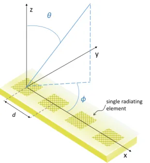
A general scheme of a transmitarray antenna is shown in Fig. 1.1. It is formed by a feed, labelled focal source, placed at a distance F, labelled focal distance, which illuminates a first array, labelled receiving layer, working in receiving mode. This array is connected or coupled through a matrix of phase shifters to another one, labelled transmitting layer, working in transmitting mode. The focal distance is selected as a trade-off between spillover losses and illumination tapering in order to maximize the gain. Each unit-cell provides the phase shift required to compensate the differential path rmfrom the source position and to
generate the desired phase distribution (Fig. 1.1).
Most of the transmitarrays proposed during the last years are based on a planar tech-nology reducing the cost of fabrication thanks to the standard PCB (Printed Circuit Board) manufacturing process. The main advantages of transmitarray antennas are the absence of
Receiving layer Transmitting layer
x z y
Incident wave Emerging wave
Variable phase shift Rx antenna
Tx antenna unit-cellm-th F
rm
Focal source
Figure 1.1: Scheme of the working principle of a transmitarray.
feed blockage area and the possibility to reduce the focal distance to obtain compact systems to mount on mobile platforms, such as aircraft, high-speed trains, etc. Controlling the phase shift given by each unit-cell, the main beam direction and shape can be changed dynami-cally and the transmitarray becomes reconfigurable. This phase shifting functionality can be implemented in different technologies and a summary of the state-of-the-art is presented in this chapter.
The competing technologies of transmitarrays are phased arrays and reflectarrays. Phased array systems are the most common antennas used in high-end radar applications. Excel-lent beam scanning capabilities are obtained with the control of the excitation phase and amplitude of each antenna element realized with complex networks, as shown in the scheme of Fig. 1.2(a), which can be implemented in different technologies. The main limitations of phased arrays are related to the design of the feed network. In fact, its complexity results in high losses which usually have to be compensated by amplifiers. In addition, this grade of complexity is directly proportional to the array size and it covers a significant share of the total costs. For electronic reconfigurable designs, high power consumption is another drawback. Quasi optical feeding systems, such as Rotman lenses, reflectarray and trans-mitarray antennas reduce the losses and complexity of the feeding network, especially for reconfigurable designs. However, phased arrays are still preferred where high performance radiation patterns characteristics are needed.
1.2. PASSIVE TRANSMITARRAYS: STATE-OF-THE-ART 39 Variable phase shifter Input signal x z y Emerging wave Single antenna Single array element Power splitter (a) Source x z y Incident wave Emerging wave
Variable phase shift
Rx/Tx antenna
unit-cell F
(b)
Figure 1.2: Scheme of the working principle of phased array (a) and reflectarray (b) antennas.
source, a horn antenna for example, as shown in the scheme of Fig. 1.2(b) [1]. By controlling the phase of the reflected waves locally with each unit-cell, it is possible to obtain the desired main beam direction and/or beam shape. Many designs based on this architecture were proposed in the last years [2, 3, 4, 5, 6, 7, 8, 9, 10, 11, 12, 13, 14]. However, the feed position introduces a blocking area which may perturb the radiated field in some applications. For this reason, tilted feed positions and sub-reflector systems are developed, similarly for the traditional parabolic reflector antennas, but this source position still limits the possibility of integration. On the other hand, the reflectarray systems facilitate the placement of the control logics for reconfigurable design on the back side of the structure.
In terms of complexity, unit-cells for transmitarray applications require more layers and then higher design complexity. However, this increases the degrees of freedom of the struc-ture making easier the introduction of advanced controls on the transmitted waves, such as the polarization. In addition, in transmitarray antennas, the feed source placed on the opposite side of the radiation surface leads to multi source illumination and reduced fo-cal distance possibilities, paving the way to integrate these antennas on vehicles, such as high-speed trains and aircrafts, leading to smart skin systems.
1.2
Passive transmitarrays: State-of-the-art
In this section, some examples of passive unit-cell and transmitarray designs proposed in the literature are presented. The main specification is usually to obtain a good transmission with different phase shifts by varying one or more dimensions of the structure. In [15], a
first simple design working in L-band is proposed. It is based on a patch loaded by two stubs printed on the transmitting layer. On the receiving layer, a ground plane with a slot is
Figure 1.3: Scheme of unit cell with two ground planes and a delay line. 5 × 5 array designed and measured radiation pattern at 12 GHz [16].
considered to feed the patch. Different phase shifts can be achieved by using multiple stubs or a multilayer structure.
The solution proposed in [16, 17] considers one rectangular patch on both sides with two different ground planes in order to obtain a high level of isolation between the receiving and transmitting layers, as shown in Fig. 1.3. The intermediate layer includes a delay line in stripline technology connected to the two patches with two metallized vias to realize the required phase shifting function. A photograph of the 5 × 5 array prototype realized at 12 GHz and the measured radiation pattern are shown in Fig. 1.3. Despite the high level of isolation, a double ground plane stacking requires a high number of layers complicating the design. In addition, undesired modes could easily propagate in the intermediate layer between the ground planes (parallel-plate modes).
A simpler stacking was considered in [19, 18]. The transmitarrays proposed in these works at X- and V-band frequencies require only two rectangular patches printed on two substrates separated by one ground plane and connected to each other with a via (Fig. 1.4). The phase shift is obtained by considering different angles of rotation of the transmitting layer patch. In this way, the frequency response of the unit-cell is the same for all the phase states and a high phase resolution can be obtained while generating a circular polarization (Fig. 1.4). This unit-cell has been also studied analytically defining a lumped elements equivalent circuit in order to simplify the design procedure. A 20 × 20 unit-cell array with four different types of unit cells with phase shifts of 0◦, 90◦, 180◦ and 270◦ (2-bit of phase quantization) is designed and tested in X-band [19]. The structure and the radiation pattern
1.2. PASSIVE TRANSMITARRAYS: STATE-OF-THE-ART 41
Figure 1.4: 3D sketch and top view of the unit cell proposed with different angles of rotation. Prototype of the transmitarray with 2-bit unit cells and radiation pattern at 10 GHz [18].
on both principal planes are shown in Fig. 1.4.
In the solution proposed in [20, 21] at 30 GHz, the resonant element of the unit-cell is formed by two concentric rings printed on a substrate. By using a double ring structure, the double resonant behaviour leads to a wider operational bandwidth. Varying the gap between the two rings or the width of the outer ring, the phase shift can be varied. The whole structure is formed by four different layers, as shown in Fig. 1.5, in order to increase the phase range. Different unit-cells are studied in this work: fixed gap and different ring dimensions, different gap between the rings, ring printed on different substrates and fixed external ring dimensions. After an optimization study, the last solution presents better performances in terms of phase variation (about 80◦) and then it is chosen to realize a prototype of a 21 × 21 transmitarray. The air gap between the different layers is equal to 0.3 wavelengths (3 mm) in order to maximize the transmission coefficient at the center frequency (30 GHz). The number of layers is chosen as the best trade off between the complexity of the whole structure and the possible phase shifts range. In particular, a range of 270◦ of
phase shift has been found with four layers. The maximum gain is 28.59 dBi at 30 GHz with a bandwidth of 2.25 GHz (7.5%) and a total radiation efficiency of 42% with the F /D ratio equal to 0.9. The measured radiation pattern is shown in the graphs of Fig. 1.5. The Side Lobes Level (SLL) is about -17 dB. The main drawback of this approach is the limited phase range achieved with a single layer that obliges to cascade several panels to extend it. This aspect limits also a possible implementation of the electronic control of the phase.

![Figure 1.6: Unit-cell based on dielectric resonator. Simulated radiation patterns in the planes φ = 0 ◦ and φ = 90 ◦ at 5.8 GHz of the transmit-array [22].](https://thumb-eu.123doks.com/thumbv2/123doknet/7773935.257383/44.892.226.726.142.486/figure-dielectric-resonator-simulated-radiation-patterns-planes-transmit.webp)
![Figure 1.12: Photograph of the M-A-F-A prototype measured in waveguide. Simulated and measured S-parameters in magnitude and phase [30].](https://thumb-eu.123doks.com/thumbv2/123doknet/7773935.257383/49.892.163.695.330.761/photograph-prototype-measured-waveguide-simulated-measured-parameters-magnitude.webp)
![Figure 1.24: Side view, top view and bottom view of the reconfigurable 1-bit unit cell based on p-i-n diodes [40].](https://thumb-eu.123doks.com/thumbv2/123doknet/7773935.257383/59.892.246.607.406.732/figure-view-view-view-reconfigurable-unit-based-diodes.webp)
![Figure 1.26: Measured gain of the transmit-array for the different phase distribution in H-plane [40].](https://thumb-eu.123doks.com/thumbv2/123doknet/7773935.257383/60.892.173.755.586.826/figure-measured-transmit-array-different-phase-distribution-plane.webp)
![Figure 1.29: Satellite channels in Ku- and Ka-band for the ITU region 1 [43].](https://thumb-eu.123doks.com/thumbv2/123doknet/7773935.257383/62.892.173.760.130.527/figure-satellite-channels-ku-ka-band-itu-region.webp)
![Figure 1.34: Experimental setup and measured path losses at 28 GHz in the experiment carried out at the NYU, US [53].](https://thumb-eu.123doks.com/thumbv2/123doknet/7773935.257383/66.892.185.766.854.1028/figure-experimental-setup-measured-path-losses-experiment-carried.webp)
![Figure 1.35: Experimental setup and measured path losses at 37.6 GHz in the experiment carried out at the University of Texas, US [53].](https://thumb-eu.123doks.com/thumbv2/123doknet/7773935.257383/67.892.143.723.149.402/figure-experimental-measured-losses-experiment-carried-university-texas.webp)