Design of Experiments on a Semiconductor Plasma
Ashing Process: Methods and Analysis
by
Tanay Rahul Nerurkar
Bachelor of Science in Engineering (Mechanical Engineering) The University of Michigan-Ann Arbor, 2015
Submitted to the Department of Mechanical Engineering in Partial Fulfillment of the Requirements for the Degree of
MASTER OF ENGINEERING IN ADVANCED MANUFACTURING AND DESIGN AT THE
MASSACHUSETTS INSTITUTE OF TECHNOLOGY SEPTEMBER 2016
© 2016 Tanay Rahul Nerurkar. All rights reserved. The author hereby grants to MIT permission to reproduce
and to distribute publicly paper and electronic copies of this thesis document in whole or in part
in any medium now known or hereafter created.
Signature of Author _____________________________________________________________ Tanay Rahul Nerurkar Department of Mechanical Engineering August 19th, 2016
Certified by____________________________________________________________________ Duane S. Boning Professor of Electrical Engineering and Computer Science Thesis Supervisor
Accepted by___________________________________________________________________ Rohan Abeyaratne Quentin Berg Professor of Mechanics
Design of Experiments on a Semiconductor Plasma
Ashing Process: Methods and Analysis
by
Tanay Rahul Nerurkar
Submitted to the Department of Mechanical Engineering on August 19th, 2016 in Partial Fulfillment of the Requirements for the Degree of
Master of Engineering in Advanced Manufacturing and Design Abstract
Characterizing and controlling process variations in semiconductor manufacturing processes is crucial to ensure the extremely low defect and scrap rates that are needed for semiconductor manufacturing companies to maximize profitability. As semiconductor device critical dimensions become smaller and chips become more complex, and with customers enquiring about process capability metrics to make sure they get the highest quality product, there is a need for chip manufacturers to thoroughly analyze and define their process capabilities. The work in this thesis done in collaboration with Analog Devices Inc., a leading chip manufacturer, shows how the concept of design of experiments (DOE) and statistical regression modeling techniques can be implemented in a practical industrial setting to rigorously understand and mathematically characterize process variations in a semiconductor fabrication process (plasma ashing).
New approaches are introduced to Analog Devices Inc. in calculating wafer statistics. Methodologies are developed that will help the company to choose the right experimental designs based on the objective (e.g. accurate prediction of the response variable, process optimization, process robustness, etc.) while taking into account the process, time, and cost constraints. Multiple regression modeling techniques are utilized to analyze the outcomes of the experiment and the results of these techniques are compared to each other in order to choose the right model needed to satisfy the objective. The statistical software JMP is used to tease out subtle implications of the outcomes of the DOE and formulate hypotheses about any anomalies. The DOEs are performed on two Gasonics Aura 3010 machines that carry out the plasma ashing process using the same process parameters in order to highlight not only the similarities but also the differences in the machines which come from factors like the intrinsic build and state of the machines. The findings and results identify opportunities for the development of new process improvement strategies, faster root cause analysis of failures, methods to systematically calibrate new equipment, update standard operating procedures, and opportunities for machine matching. The purpose of this thesis is to serve as a pedagogical document and template for the process engineers at Analog Devices Inc. in the future to perform DOEs on other processes and machines in the fabrication center.
Thesis Supervisor: Duane S. Boning
Acknowledgements
The success of this project and thesis would not have been possible without the tremendous support and guidance of my advisors Prof. Duane S. Boning (MIT), Ken Flanders (Analog Devices Inc.), and Jack Dillon (Analog Devices Inc.). I would like to thank them for giving me such a fantastic opportunity and allowing me to work with them and learn from them. Thank you to my teammates Tan Nilgianskul and Feyza Haskaraman for their ideas and collaboration throughout this project that made my work in this thesis even better and working with them has been a truly fabulous experience.
I owe a deep sense of gratitude towards the process engineering and equipment engineering teams at Analog Devices Inc. especially Megan Kromer, Pam Petzold, Peter Cardillo, Rich DeJordy, Dale Shields, and Brian Chouinard. They have all gone to great lengths in making sure I had access to all the tools and equipment in the fab whenever I needed them, and that I was properly given training on operating the machines.
I would like to thank Jose Pacheco, Prof. David Hardt, and Dr. Brian Anthony for believing in me and allowing me to pursue my graduate degree at MIT. The students, faculty, and staff that I have met and collaborated with in my cohort and the Institute in general have truly challenged me and encouraged me to develop skills and pursue opportunities beyond my wildest imaginations, and I leave Cambridge with many fond memories and lifelong friendships.
I would also like to thank Prof. Dawn Tilbury, Prof. Kira Barton, Nicholas Putman, and Miguel Saez at the University of Michigan for introducing me to many exciting research problems in manufacturing that made my decision to pursue graduate studies in the topic an easy one. I would also like to thank Prof. Allen Liu at the University of Michigan for his advice and guidance in helping me choose a graduate program that would match my needs and career ambitions.
Lastly but most importantly a big thank you to my family, especially my parents Rahul and Ashwini Nerurkar and my sister Shilarna Nerurkar, who have made many sacrifices to ensure I got the best possible education.
Table of Contents
CHAPTER 1: INTRODUCTION ... 15
1.1 BACKGROUND INFORMATION ON ANALOG DEVICES INC. ... 15
1.2 GENERAL SEMICONDUCTOR FABRICATION PROCESS ... 16
1.3 PLASMA ASHING PROCESS ... 17
1.4 THE GASONICS AURA 3010 PLASMA ASHING MACHINE ... 18
1.5 PARTIAL RECIPE AND PROCESS PARAMETERS ... 20
1.6 DATA COLLECTION AND LOGGING ... 23
1.7 CALCULATION OF BASIC STATISTICS ... 25
1.8 PROBLEM STATEMENT ... 27
1.9 OUTLINE OF THESIS ... 29
CHAPTER 2: THEORETICAL REVIEW OF KEY CONCEPTS ... 30
2.1 STATISTICAL PROCESS CONTROL ... 30
2.1.1 Origin of SPC ... 30
2.1.2 Shewhart Control Charts ... 31
2.2 ANALYSIS OF VARIANCE ... 32
2.3 DESIGN OF EXPERIMENTS ... 35
2.4 STATISTICAL HYPOTHESIS TESTING ... 37
2.4.1 Z-Test for Detecting Mean Shift ... 37
2.4.2 F-test ... 39
2.4.3 Bartlett’s Test ... 40
CHAPTER 3: DESIGN OF EXPERIMENTS - METHODOLOGY ... 42
3.1 MOTIVATION AND NEED FOR DESIGN OF EXPERIMENTS ... 42
3.2 A STANDARD METHODOLOGY FOR DESIGN OF EXPERIMENTS ... 44
3.3 EXPERIMENTAL DESIGNS FOR LINEAR MODELS ... 47
3.4 EXPERIMENTAL DESIGNS FOR NON-LINEAR MODELS ... 52
CHAPTER 4: DESIGN OF EXPERIMENTS - ANALYSIS ... 54
4.1 G53000: MULTIPLE RESPONSE SURFACE MODEL ... 54
4.2 G53000: SINGLE RESPONSE SURFACE MODEL ... 68
4.5 G63000: SINGLE RESPONSE SURFACE MODEL ... 90
4.6 G63000: QUADRATIC RESPONSE SURFACE MODEL ... 95
4.8 COMPARISON BETWEEN G53000 AND G63000 MACHINES ... 101
CHAPTER 5: CONTRIBUTIONS TO ANALOG DEVICES INC. ... 102
5.1 NEW METHODOLOGIES FOR WAFER STATISTICS CALCULATION ... 102
5.2 ROOT CAUSE ANALYSIS AND MACHINE DIAGNOSTICS ... 104
5.3 PROCESS IMPROVEMENT STRATEGIES ... 112
CHAPTER 6: CONCLUSION AND FUTURE WORK ... 114
6.1 CONCLUSION ... 114
6.2 FUTURE WORK ... 114
List of Figures
Figure 1-1: Overview of manufacturing operations at Analog Devices Inc.’s facilities. ... 16
Figure 1-2: General semiconductor fabrication process ... 17
Figure 1-3: Schematic of the plasma ashing process. ... 18
Figure 1-4: A file photo of the Gasonics tool. ... 19
Figure 1-5: A sample recipe on the display screen of the Gasonics tool. ... 21
Figure 1-6: Spatial distribution of the nine measured sites on a wafer. ... 23
Figure 1-7: Co-ordinate values of the nine measured sites on a wafer. ... 23
Figure 1-8: Areal Representation Ratio of nine sites on the wafer. ... 25
Figure 1-9: An example of within-wafer non-uniformity and run-to-run variation observed on the plasma ashing process. ... 27
Figure 1-10: X-bar control chart monitoring the plasma ashing process showing clear mean shifts. ... 28
Figure 2-1: Example of a Shewhart control chart. ... 31
Figure 3-1: Plasma ashing process block diagram. ... 43
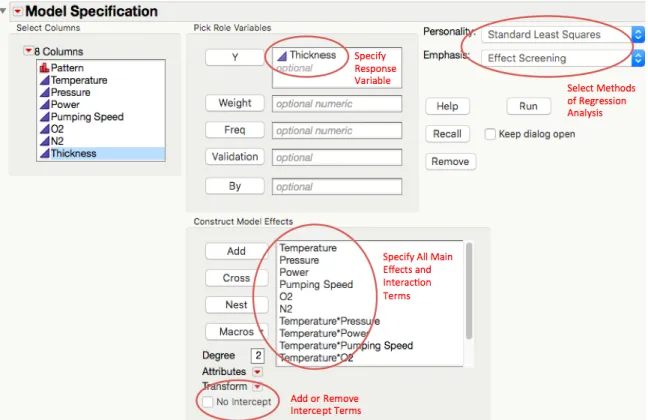
Figure 4-1: Specifying model parameters in JMP. ... 56
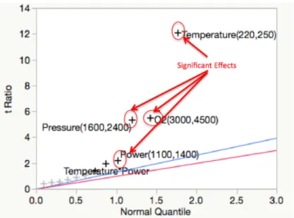
Figure 4-2: Normal probability plot of effects affecting photoresist strip rate standardized to have equal variances across all runs in the G53000 machine. ... 57
Figure 4-3: Normal probability plot of effects affecting photoresist strip rate not standardized that have unequal variances across all runs in G53000 machine. ... 57
Figure 4-4: Singularity report as seen in JMP. ... 58
Figure 4-5: Observed values versus model predicted values plot for amount of photoresist removed from site 3 of the wafer in the G53000 machine. ... 59
Figure 4-6: Model coefficients and hierarchy of significance of factors affecting the amount of photoresist removed from a wafer in the G53000 machine (site 3 of wafer). ... 60 Figure 4-7: Normal probability plot of residuals for amount of photoresist removed from a wafer in the G53000 machine (site 3). ... 63 Figure 4-8: Residual versus predicted plot for amount of photoresist removed from a wafer in the G53000 machine (site 3). ... 63 Figure 4-9: Observed and predicted values of the amount of photoresist stripped at each site for treatment combination [--+-++].. ... 67 Figure 4-10: Observed and predicted values of the amount of photoresist stripped at each site for treatment combination [00+000] ... 67 Figure 4-11: Observed and predicted values of the amount of photoresist stripped at each site for treatment combination [+---+-] ... 67 Figure 4-12: Observed and predicted values of the amount of photoresist stripped at each site for treatment combination [+0+0+0] ... 67 Figure 4-13: Normal probability plot of effects affecting wafer non-uniformity standardized to have equal variances across all runs in the G53000 machine. ... 70 Figure 4-14: Observed values versus model predicted values plot for the wafer non-uniformity observed on the G53000 machine. ... 71 Figure 4-15: Model coefficients and hierarchy of significance of factors affecting the wafer uniformity observed on the G53000 machine. ... 71 Figure 4-16: Normal probability plot of residuals for wafer non-uniformity observed on the G53000 machine. ... 72 Figure 4-17: Residual versus predicted plot for wafer non-uniformity observed on the G53000 machine. ... 72 Figure 4-18: Observed values versus model predicted values plot for the wafer non-uniformity quadratic model obtained from the experiments done on the G53000 machine. ... 76
Figure 4-19: Quadratic model coefficients of factors affecting the wafer non-uniformity observed on the G53000 machine. ... 76 Figure 4-20: Normal probability plot of residuals for wafer non-uniformity observed on the G53000 machine (quadratic model). ... 77 Figure 4-21: Residual versus predicted plot for wafer non-uniformity observed on the G53000 machine (quadratic model). ... 77 Figure 4-22: Quadratic response surface for wafer non-uniformity with temperature and oxygen as controllable factors obtained from the experiments done on the G53000 machine. ... 79 Figure 4-23: Prediction profiler for the response of wafer non-uniformity to temperature and oxygen for the G53000 machine. ... 79 Figure 4-24: Normal probability plot of effects affecting photoresist strip rate standardized to have equal variances across all runs in the G63000 machine. ... 81 Figure 4-25: Observed values versus model predicted values plot for amount of photoresist removed from site 3 of the wafer in the G63000 machine. ... 82 Figure 4-26: Model coefficients and hierarchy of significance of factors affecting the amount of photoresist removed from a wafer in the G63000 machine (site 3 of wafer.) ... 83 Figure 4-27: Normal probability plot of residuals for amount of photoresist removed from a wafer in the G63000 machine (site 3). ... 86 Figure 4-28: Residual versus predicted plot for amount of photoresist removed from a wafer in the G63000 machine (site 3). ... 86 Figure 4-29: Observed and predicted values of the amount of photoresist stripped at each site for treatment combination [-++---] ... 89 Figure 4-30: Observed and predicted values of the amount of photoresist stripped at each site for treatment combination [000000]. ... 89 Figure 4-31: Observed and predicted values of amount of the photoresist stripped at each site for treatment combination [++-+--]. ... 89
Figure 4-32: Observed and predicted values of amount of the photoresist stripped at each site for treatment combination [++++++]. ... 89 Figure 4-33: Normal probability plot of effects affecting wafer non-uniformity standardized to have equal variances across all runs in the G63000 machine. ... 91 Figure 4-34: Observed values versus model predicted values plot for the wafer non-uniformity observed on the G63000 machine. ... 92 Figure 4-35: Model coefficients and hierarchy of significance of factors affecting the wafer
non-uniformity observed on the G63000 machine. ... 93 Figure 4-36: Normal probability plot of residuals for wafer non-uniformity observed on the G63000 machine. ... 94 Figure 4-37: Residual versus predicted plot for wafer non-uniformity observed on the G63000 machine. ... 94 Figure 4-38: Observed values versus model predicted values plot for the wafer non-uniformity quadratic model obtained from the experiments done on the G63000 machine. ... 97 Figure 4-39: Quadratic model coefficients of factors affecting the wafer non-uniformity observed on the G63000 machine. ... 97 Figure 4-40: Normal probability plot of residuals for wafer non-uniformity observed on the G63000 machine (quadratic model). ... 98 Figure 4-41: Residual versus predicted plot for wafer non-uniformity observed on the G63000 machine (quadratic model). ... 98 Figure 4-42: Quadratic response surface for wafer non-uniformity with temperature and oxygen as controllable factors obtained from the experiments done on the G63000 machine. ... 100 Figure 4-43: Prediction profiler for the response of wafer non-uniformity to temperature and oxygen for the G63000 machine. ... 100 Figure 5-1: Spatial map of a wafer showing the distribution of sites ... 103
Figure 5-2: 3-D plot of a wafer showing the amount of photoresist removed at each of the 49 sites ... 103 Figure 5-3: Spatial distribution map of a wafer processed in the G53000 machine using the partial recipe. ... 105 Figure 5-4: Map of the amount of photoresist removed from the wafer sites shown in Figure 5-3.
... 105 Figure 5-5: Temperature profile of a wafer being processed in the G53000 machine using the partial recipe. ... 106 Figure 5-6: Spatial map of wafer processed in the G63000 machine using the partial recipe. .. 107 Figure 5-7: Temperature profile of a wafer being processed in the G63000 machine using the partial recipe. ... 107 Figure 5-8: Flat effect on wafer processed in the G53000 machine using the partial recipe. .... 109 Figure 5-9: Flat effect on wafer processed in the G63000 machine using the partial recipe. .... 109 Figure 5-10: Amount of photoresist removed from each site in the plasma ashing process using the partial recipe on the G53000 machine. ... 110 Figure 5-11: Amount of photoresist removed from each site in the plasma ashing process using the partial recipe on the G63000 machine. ... 110 Figure 5-12: Prediction profiler for the amount of photoresist removed from site 1 of the wafer in the G53000 machine. ... 111
List of Tables
Table 1-1: Controllable process parameters of the partial recipe. ... 22
Table 1-2: Nanospec data logging spreadsheet. ... 24
Table 2-1: A standard ANOVA table for a single factor fixed effect model. ... 33
Table 2-2: 23 full factorial experimental design. ... 36
Table 2-3: 23-1 factorial experimental design. ... 37
Table 3-1: The controllable factors and the levels at which they are run. ... 48
Table 3-2: The 26-2 resolution IV factorial design run table. ... 48
Table 3-3: The controllable factors and specific levels at which the 32 full factorial experiments are run. ... 53
Table 3-4: 32 full factorial design run table. ... 53
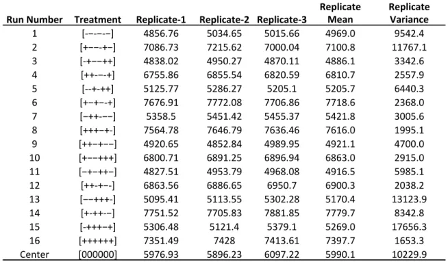
Table 4-1: Values of replicate runs, replicate mean, and replicate variance for amount of photoresist stripped from a wafer in the G53000 machine. ... 55
Table 4-2: Adjusted R2 values for observed versus predicted plot for the amount of photoresist removed from all sites on a wafer in the G53000 machine. ... 60
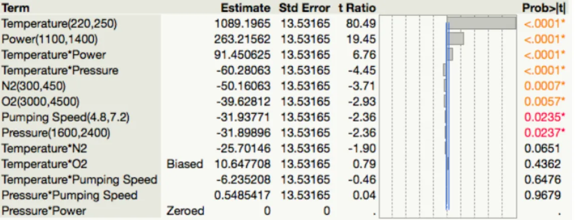
Table 4-3: Model coefficients for all nine sites for the amount of photoresist removed from a wafer in the G53000 machine. ... 61
Table 4-4: List of significant two factor interactions for the amount of photoresist removed from a wafer in the G53000 machine. ... 62
Table 4-5: Test cases for a variety of treatment combinations to validate the wafer non-uniformity model using the multiple response surface method. ... 65
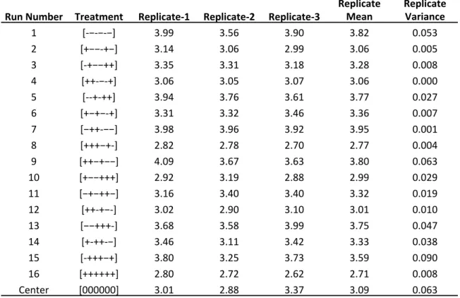
Table 4-6: Values of replicate runs, replicate mean, and replicate variance for wafer non-uniformity observed on the G53000 machine. ... 69
Table 4-7: Test cases for a variety of treatment combinations to validate the wafer non-uniformity model using the single response surface method on the G53000 machine. ... 73
Table 4-8: Values of wafer non-uniformity obtained from the 32 full factorial experimental runs done on the G53000 machine. ... 75 Table 4-9: Test cases for a variety of treatment combinations to validate the wafer
non-uniformity quadratic model obtained from the experiments done on the G53000 machine. 78 Table 4-10: Values of replicate runs, replicate mean, and replicate variance for amount of photoresist stripped from a wafer in the G63000 machine. ... 80 Table 4-11: Adjusted R2 values for observed values versus predicted values plot for the amount of photoresist removed from all sites on a wafer in the G63000 machine. ... 83 Table 4-12: Model coefficients for all nine sites for the amount of photoresist removed from a wafer in the G63000 machine. ... 84 Table 4-13: List of significant two factor interactions for the amount of photoresist removed from a wafer in the G63000 machine. ... 85 Table 4-14: Test cases for a variety of treatment combinations to validate wafer non-uniformity model obtained from the experiments done on the G63000 machine. ... 87 Table 4-15: Values of replicate runs, replicate mean, and replicate variance for wafer
non-uniformity observed on the G63000 machine. ... 90 Table 4-16: Test cases for a variety of treatment combinations to validate the wafer
non-uniformity model using the single response surface method from the experiments done on the G63000 machine. ... 95 Table 4-17: Values of wafer non-uniformity obtained from the 32 full factorial experimental runs in the G63000 machine. ... 96 Table 4-18: Test cases for a variety of treatment combinations to validate the wafer
non-uniformity quadratic model obtained from the experiments done on the G63000 machine. 99 Table 5-1: Statistics of nine month actual production data from the Gasonics tools with proposed control limits. ... 108
Chapter 1: Introduction
The work in this thesis presents a methodology to systematically perform design of experiments (DOE) analyses on a semiconductor plasma ashing process. It lays out the necessary tools required to build a statistical regression model and demonstrates potential implications and analyses that could be used to better understand, improve or optimize the process for various parameters of interest. This is an industrial thesis and the work was done in collaboration with Analog Devices Inc. in their Wilmington, MA fabrication center. Analog Devices Inc. is a world leader in the design, manufacture, and marketing of high performance analog, mixed-signal, and digital signal processing integrated circuits used in a broad range of electronic applications and is headquartered in Norwood, MA [1]. Currently, there is a need in the company to rigorously analyze various processes and machine capabilities in an effort to improve yield, throughput, and reduce machine downtime through early detection of equipment anomalies. The purpose of this chapter is to provide background information on Analog Devices Inc., an introduction to the plasma ashing process that was studied in this work, and the problem statement that this thesis attempts to address.
1.1 Background Information on Analog Devices Inc.
Analog Devices Inc. is an American multinational company that specializes in the design, manufacture, and marketing of high performance analog, mixed-signal, and digital signal processing integrated circuits used in a broad range of electronic applications. The company’s products play a fundamental role in converting, conditioning, and processing real-world phenomena such as temperature, pressure, sound, light, speed, and motion into electrical signals to be used in a wide array of electronic devices [2].
The company was founded in 1965 by Ray Stata and Matthew Lorber and is headquartered in Norwood, MA. Analog Devices Inc. has operations in 23 countries and serves over 100,000 customers from various industries like consumer electronics, automotive, and defense to name a few. The annual revenue of the company in the fiscal year 2015 was
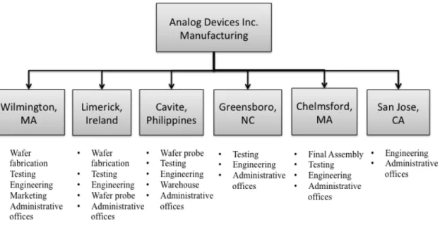
The manufacturing and assembly of Analog Devices Inc.’s products is conducted in several locations worldwide. Figure 1-1 [2] shows an overview of the location and functions of the company’s manufacturing and assembly facilities.
Figure 1-1: Overview of manufacturing operations at Analog Devices Inc.’s facilities.
The experiments in this thesis are carried out on the Gasonics Aura 3010 plasma ashing process tools in the Wilmington, MA fabrication center. This thesis is written in conjunction with the works of Tan Nilgianskul [3] and Feyza Haskaraman [4], and several sections and descriptions in this thesis are written in common with their works.
1.2 General Semiconductor Fabrication Process
Pre-doped wafers are supplied to the Wilmington, MA fabrication center as the starting material. The Wilmington, MA fabrication site is divided into five main sub-departments: thin-films, etch, photolithography, diffusion, and CMP (chemical mechanical polymerization). A key procedure used at many points in the manufacturing of a device is photolithography where photoresist is deposited and patterned on the surface of the wafer. In photolithography, photoresist is spun onto the wafer surface and exposed and developed to create open access to
the surface in some regions, and in other regions the photoresist remains as a blocking mask. The diffusion team then selectively implants impurity ions or the thin-films group deposits metals onto the designated parts of the silicon wafer. The etch group then strips the unwanted photoresist off from these wafers. The function of the CMP group is to use chemical-mechanical reaction techniques to smoothen the surface of the deposited materials. Figure 1-2 [5] gives an overview of the steps and processes involved in semiconductor fabrication.
Figure 1-2: General semiconductor fabrication process.
These procedures do not have to go in any particular order. Different types of devices require different configurations of material layers with repeated sequences of photolithography, etch, implantation, deposition, and other process steps. The flexibility of these process steps is what enables the fabrication center to produce customizable electronic parts on a customer’s short-term order.
1.3 Plasma Ashing Process
For the purpose of this thesis, the plasma ashing process is investigated. This process is used to remove photoresist (light sensitive mask) from an etched wafer using a monoatomic reactive species that reacts with the photoresist to form ash, which is removed from the vicinity of the wafer using a vacuum pump. The reactive species is generated by exposing a gas such as
oxygen or fluorine to high power radio or microwaves, which ionizes the gas to form monoatomic species [6], [7]. Figure 1-3 [6] shows a general schematic of the plasma ashing process with the key components indicated.
Figure 1-3: Schematic of the plasma ashing process.
Analog Devices Inc. uses the Gasonics Aura 3010 machines (hence forth will be referred to as Gasonics tools or Gasonics machines) to carry out the plasma ashing process. The reactive gas used by the company is oxygen and microwaves are used to ionize the gas. The Gasonics tool allows for the change of several variables including wafer temperature, chamber pressure, and power that make up a recipe to allow for different photoresist removal rates that may be needed for different products.
1.4 The Gasonics Aura 3010 Plasma Ashing Machine
The Gasonics Aura 3010 machine is used by Analog Devices Inc.’s Wilmington, MA fabrication center for photoresist ashing and cleaning of semiconductor wafers by creating a low-pressure and low-temperature glow discharge, which reacts chemically with the surface of the wafer [8]. The Gasonics system is composed of three main components:
i. The reactor chamber that contains the system controller, the electro-luminescent display, wafer handling robot, the microwave generator, and the gas box.
ii. The power enclosure wall box. iii. The vacuum pump.
Figure 1-4 [9] below shows a picture of the Gasonics Aura 3010 machine.
Figure 1-4: A file photo of the Gasonics tool.
The machine is equipped with a three axis of motion wafer handling robot that picks up a single wafer from a twenty five wafer holding cassette and places it in the process chamber to execute the photoresist stripping process. After a particular recipe is executed, the robot removes the wafer and places it on a cooling station if required before returning the wafer back to its slot in the cassette. Inside the process chamber, the wafer rests on three sapphire rods and a closed loop temperature control (CLTC) probe which includes a thermocouple to measure the temperature of the wafer during the ashing process. Twelve chamber cartridges embedded in the chamber wall heat the process chamber. During the plasma ashing process, eight halogen lamps heat the wafer to the required process temperature. The process gases (oxygen or nitrogen) are mixed and delivered to a quartz plasma tube in the waveguide assembly where microwave energy generated by a magnetron ionize the gases into the monoatomic reactive species. The
machine is designed in a way to only allow the lower-energy free radicals and neutrals to come in contact with the wafer surface as higher energy radicals can damage the wafer. After the wafer has been stripped, the halogen lamps, microwave power, and the process gas flows are turned off and the process chamber is then purged with nitrogen before being vented to the atmosphere for wafer removal. The door to the process chamber is then opened and the robot removes the wafer to either place it on the cooling station or put it back in the cassette slot [8].
Analog Devices Inc.’s Wilmington, MA fabrication center has seven Gasonics machines which have a codename of GX3000 where X is a number between 1 and 7. The experiments and analysis that are presented in this work were conducted on G53000 and G63000 machines.
1.5 Partial Recipe and Process Parameters
A recipe is defined as a set of input settings that can be adjusted over an operating range on a tool or machine to execute a desired manufacturing process at those settings. For example, consider Figure 1-5 [8] which shows a sample recipe on the display screen of the Gasonics machine. The machine allows the operator to vary the quantities under the column “PARAMETER”. The process engineers in the company are responsible for proposing and executing an optimal recipe taking into account product quality, throughput, and cost constraints. In addition to designing recipes for production wafers, Analog Devices Inc. also designs recipes to run qualification tests. Qualification tests are used to periodically monitor product quality and verify machine calibrations. In this thesis, the qualification test recipe that has been studied is named “partial” by Analog Devices Inc.
Figure 1-5: A sample recipe on the display screen of the Gasonics tool.
The partial recipe is used as a qualification test to calibrate the rate of photoresist removal on the Gasonics machine. The recipe is designed such that the photoresist mask is not completely removed from the wafer after the process. This is intentionally done so that the amount of photoresist removed and the time taken to do so can be recorded. An ideal Gasonics machine would remove 6000 Angstroms of resist in eight seconds. The entire process with the partial recipe takes approximately 63 seconds with the first 20 seconds being allocated to heating the wafer to the necessary conditions and bringing the machine to steady state (step-1), the next eight seconds being allocated to the stripping process (step-2), and the last 35 seconds being allocated to cooling the wafer. Table 1-1 shows the necessary machine parameters needed for the partial recipe.
Table 1-1: Controllable process parameters of the partial recipe.
The description of the partial recipe process parameters listed in Table 1-1 is as follows:
i. Temperature: This is the temperature to which the wafer is heated to and maintained
during the plasma ashing process.
ii. Pressure: This is the pressure of the gases present inside the reacting chamber of the
Gasonics machine during the plasma ashing process.
iii. Power: This is the power needed by the magnetron to generate the necessary
microwave energy to ionize the reacting gases.
iv. Blower and Main Vacuum Pump Speeds: The main vacuum pump speed refers to
the rate at which the residue ash and excess gases are removed from the reacting chamber. The blower pump is an addition to the main pump aiding in increasing the removal rate of the residue ash and gases. The speed of the main pump is kept constant while the speed of the blower pump is varied from recipe to recipe.
v. Oxygen Gas Flow: This is the rate at which oxygen gas is allowed to flow into the
reacting chamber during the process. The unit of measurement is standard cubic centimeter per minute (SCCM)
vi. Nitrogen Gas Flow: This is the rate at which nitrogen gas is allowed to flow into the
reacting chamber during the process. The unit of measurement is SCCM.
vii. Step Term: This is the duration of each step in the plasma ashing process. Machine Parameter Step-1 Step-2
Temperature (Celsius) 215 235 Pressure (mTorr) 2000 2000 Power (Wa9s) 0 1400 Blower Vacuum Pump Speed (k/min) 6 6 Main Vacuum Pump Speed (k/min) 5.5 5.5 Oxygen Gas Flow (SCCM) 3750 3750 Nitrogen Gas Flow (SCCM) 375 375 Step Term (Seconds) 20 8
1.6 Data Collection and Logging
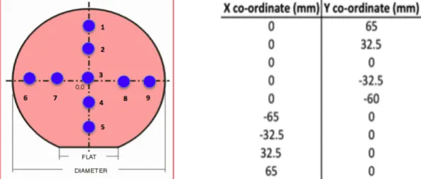
The key parameters that need to be measured in the plasma ashing process are the amount of photoresist removed from the wafer and the wafer non-uniformity after the process has been completed. The amount of photoresist removed divided by the time for which the Gasonics tool was set to function gives the photoresist removal rate, which Analog Devices Inc. uses to infer machine health. The tool used to measure the amount of photoresist removed in Analog Devices Inc.’s Wilmington fabrication center is the Nanospec 9200 measuring tool (Nanospec). The Nanospec tool has the capability to accurately measure wafer thicknesses in the Angstrom range. The Nanospec tool is programmed to measure nine sites on each wafer. Figures 1-6 and 1-7 shows the spatial distribution as well as the co-ordinate ordered pair values of the nine sites on each wafer. In the spatial distribution diagram, the blue dots indicate the sites where the measurements are taken.
Figure 1-6: Spatial distribution of the nine measured sites on a wafer.
Figure 1-7: Co-ordinate values of the nine measured sites on a wafer.
The measurement procedure of the thickness of the photoresist of the nine sites using the Nanospec tool is as follows:
i. The thickness of the photoresist is measured and recorded before the wafer undergoes the plasma ashing process. These are known as “pre-measurements”.
ii. The thickness of the photoresist is measured and recorded after the wafer undergoes the plasma ashing process. These are known as “post-measurements”.
iii. The difference between the pre-measurements and post-measurements gives the amount of photoresist removed during the process.
iv. The amount of photoresist removed can be divided by the duration of the plasma ashing process to give the rate of resist removal. The duration of the plasma ashing process is included as an input and monitored by the Gasonics tool.
The amount of photoresist removed for each of the nine sites on a single wafer is recorded in an excel spreadsheet on which further analysis can done. An example of the excel spreadsheet can be seen in Table 1-2. In Table 1-2, the columns in the spreadsheet represent the measurements taken on the nine sites within a single wafer while the rows represent different wafers measured. The Nanospec tool also logs the date and time of the measurement, which is very useful in anomaly detection.
1.7 Calculation of Basic Statistics
The raw data collected from the Nanospec 9200 tool as shown in Table 1-2needs to be manipulated further in order to make meaningful implications of the underlying trends and patterns. This section introduces the method that is used to calculate three statistical quantities:
i. The mean thickness of the nine sites on a single wafer (𝑥∗)
ii. The standard deviation of the nine sites on a single wafer (𝑠) iii. The wafer non-uniformity parameter (NU)
The nine sites that the Nanospec 9200 tool measures on a single wafer are distributed in a radial pattern from the center as can be seen in the spatial distribution diagram in Figure 1-6. Generally, in a radial distribution wafer measuring pattern, the calculation of any statistics on the sites measured on a wafer have to take into account the wafer area represented by each site for accurate analysis [10]. Figure 1-8shows the wafer areal representation of each site on a nine site radial distribution pattern. The wafers used for the purposes of this study have a diameter of six inches. 1 2 5 4 6 7 8 9 3
In Figure 1-8, site 3 represents the area bounded by the green circle (4% of the total wafer area), sites 2, 4, 7, and 8 each represent the area bounded by the red segments (32% of the total wafer area), and sites 1, 6, 5, and 9 each represent the area bounded by the orange segments (64% of the total wafer area).
The mean (𝑥∗) [11] taking into account the areal representation of each site is calculated
as follows: 𝑥∗ = !!!!𝑤!𝑥! 𝑤! ! !!! Equation 1-1
where 𝑥! is the wafer thickness measured at each site, 𝑤! is the weighted area associated with that site and 𝑁 is the number of sites.
The standard deviation (𝑠) [11] taking into account the areal representation of each site is calculated as follows: 𝑠 = !!!!𝑤! 𝑤! ! !!! !− !!!!𝑤!! ∙ 𝑤! 𝑥! − 𝑥∗ ! ! !!! Equation 1-2
where 𝑥! is the wafer thickness measured at each site, 𝑤! is the weighted area associated with that site, 𝑁 is the number of sites, and 𝑥∗ is the mean.
The wafer non-uniformity parameter (NU) [12] taking into account the areal representation of each site is calculated as follows:
𝑁𝑈 = 𝑠 𝑥∗
Equation 1-3
where 𝑠 is the standard deviation and 𝑥∗is the mean. The wafer non-uniformity parameter will be
1.8 Problem Statement
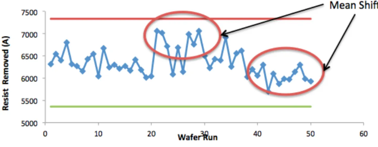
Semiconductor fabrication facilities need to maintain extremely high yields in order to maximize profitability. As a result, fabrication centers need to have a thorough understanding of their process capabilities and implement strategies that will minimize process variations to the best of their ability. Characterization and control of process variations in semiconductor manufacturing processes is the most challenging and crucial aspect for any fabrication facility given the dimensions (nanometers) at which chips are currently made. Small process variations can completely destroy modern devices. Moreover, many etching and deposition processes have multiple inputs and process steps where each input and process step can be a source of variation. This can quickly lead to a variation stack up if process control methods are not implemented appropriately. In semiconductor manufacturing, process variations manifest in multiple and interconnected ways, including variations observed within each wafer (wafer non-uniformity), variations between wafers (run-to-run), variations between batches of wafers (batch-to batch), and variation between machines executing the same process with the same parameters (machine-to-machine). An example of wafer non-uniformity and run-to-run variation in the plasma ashing process done on a Gasonics machine is shown in Figure 1-9. The columns represent the amount of photoresist removed at each site on a wafer while the rows represent the measurements taken on different wafers. The ideal scenario is that a target of 6000 Angstroms of photoresist stripped is achieved on every site of every wafer.
Figure 1-9: An example of within-wafer non-uniformity and run-to-run variation observed on the plasma ashing process.
The combined effect of the shrinking of device critical dimensions, increase in component density per chip, and more complex functionality requirements has resulted in semiconductor manufacturers needing to seek new methods to continuously monitor, update, and improve their process capabilities. Analog Devices Inc. is in a similar situation where the company is revaluating its current process control capabilities and wants to incorporate newer methods including real-time process control, automatic feedback control, and cloud-based analytics to improve its process monitoring capabilities. Currently the company uses traditional control charts to monitor its processes, but the process engineers at the company are convinced that the current charts are deficient in timely detection of unnatural drifts and mean shifts that could have negative consequences on future product lines. An “x-bar” control chart for tracking the average amount of photoresist removed during the plasma ashing process on the Gasonics tool with the current control limits is shown in Figure 1-10. There are clear mean shifts and variations are as high as 20% in the process that are not being detected by the current limits which is a cause of concern.
Figure 1-10: X-bar control chart monitoring the plasma ashing process showing clear mean shifts.
The goal of this project is to introduce Analog Devices Inc. to new process control methodologies that will provide them with a rigorous analysis and understanding of their current
process capabilities on the plasma ashing process done on the Gasonics tool. The three main areas of focus are as follows:
i. Recalculate and propose new control limits on current charts or develop new charts monitoring new variables that are a true representation of the natural variation of the plasma ashing process (Nilgianskul’s thesis [3]).
ii. Characterize and quantify the response of the amount of photoresist removed and the spatial uniformity of the wafer in the plasma ashing process with respect to the controllable input parameters on an individual machine basis (The focus of this thesis). iii. Compare the performance of two Gasonics machines and propose machine-matching
strategies to reduce or eliminate the differences in their performances and ensure that the machines function at their optimal level (Haskaraman’s thesis [4]).
Analog Devices Inc. will then use the proposed methods, results, and findings to improve process capabilities on other tools and processes in the fabrication center.
1.9 Outline of Thesis
Chapter 1 is the introduction that provides background information on Analog Devices Inc. and introduces the reader to general semiconductor fabrication processes, the plasma ashing process, and the problem statement that this thesis aims to address. Chapter 2 provides a theoretical review of the key concepts and mathematical techniques of statistical process control, design of experiments, and statistical hypothesis testing which have been compiled from various literature sources. Chapter 3 discusses the motivation, the methods, and the reasoning behind selecting the necessary experimental designs and formulating the statistical regression models that can predict the behavior of the response variable to a high degree of confidence over a range of the controllable factors. Chapter 4 provides a comprehensive analysis on the outcomes of the experiments performed using the methods outlined in Chapter 3. Chapter 5 outlines the specific contributions made to Analog Devices Inc. from the insights obtained from the design of experiments analysis. Chapter 6 presents the conclusion of the thesis and the scope for future work.
Chapter 2: Theoretical Review of Key Concepts
This chapter will give a brief introduction to the theory behind key concepts that are relevant to the construction of this thesis and the overall project in general. The ideas presented in this chapter have been compiled from a variety of literature sources. The key topics described are statistical process control, analysis of variance, design of experiments, and statistical hypothesis testing.
2.1 Statistical Process Control
Statistical process control (SPC) is used to monitor and control variations in a manufacturing process. Controlling process variations is important in a manufacturing environment because decreased variability in a process reduces scrap and rework rates leading to lower costs and improved product quality.
2.1.1 Origin of SPC
Walter A. Shewhart at Bell Laboratories introduced the SPC method in the early 1920s. Later in 1924, Shewhart developed the control chart and coined the phrase “a state of statistical control” which can actually be derived from the concept of exchangeability developed by logician William Ernest Johnson in the same year in one of his works called Logic, Part III: The
Logical Foundations of Science [13]. The theory was first put in use in 1934 at the Picatinny
arsenal, an American military research and manufacturing facility located in New Jersey. After seeing the success of this project, the US military further enforced statistical process control methods among its other divisions and contractors during the outbreak of the Second World War [14].
2.1.2 Shewhart Control Charts
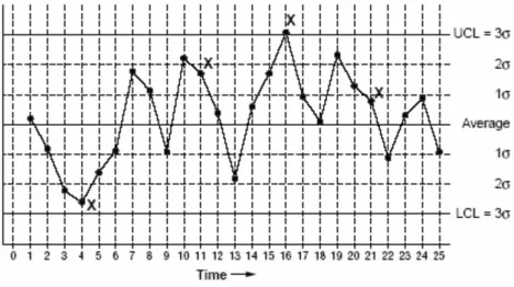
A Shewhart control chart plots a measured parameter that is an indicator of the process performance over a period of time. These plots are then bounded by control limits which are, as a rule-of-thumb, three standard deviations away from the mean on either side. An example of a control chart is shown in Figure 2-1 [15].
Figure 2-1: Example of a Shewhart control chart. Points marked with X’s are points that would be rejected based on Western Electric rules.
Control charts can either be plotted as a run chart or an x-bar chart. The run chart plots each measurement separately while the x-bar control chart plots the average of several measurements. Other statistics like variance, range, and standard deviation are also plotted in addition to the x-bar chart.
The goal of plotting control charts is to monitor the state of the manufacturing process and detect when it is out of control. Assuming that the data plotted is normally distributed, which is the case for most processes, the chance that any single point would lie above the upper control limit (UCL) or below the lower control limit (LCL) (three standard deviations above or below the mean) would be less than 0.3%. Assuming that a set of data is normally distributed with mean µ and variance σ 2, UCL and LCL can be expressed as:
𝑈𝐶𝐿 = 𝜇 + 3𝜎
Equation 2-1
𝐿𝐶𝐿 = 𝜇 − 3𝜎
Equation 2-2
The probability of a point lying beyond the limits for any normally distributed data set can be solved for. 𝑃 𝑋 > 𝑈𝐶𝐿 = 𝑃 𝑍 >𝑈𝐶𝐿 − 𝜇 𝜎 = 𝑃 𝑍 > 3 ≈ 0.0013 𝑃 𝑋 < 𝑈𝐶𝐿 = 𝑃 𝑍 <𝜇 − 𝐿𝐶𝐿 𝜎 = 𝑃 𝑍 < 3 ≈ 0.0013 𝑃(𝑋 > 𝑈𝐶𝐿| 𝑋 < 𝐿𝐶𝐿 = 𝑃 𝑋 > 𝑈𝐶𝐿 + 𝑃 𝑋 < 𝐿𝐶𝐿 ≈ 0.0013 + 0.0013 ≈ 0.0027 𝑃(point lies outside control limit) ~ 0.3%
Equation 2-3
Besides the upper and lower control limit rule, there are other rules (Western Electric) that could be used as guidelines to suspect when the process is out of control. These include 1) if two out of three consecutive points lie either two standard deviations above or below the mean 2) four out of five consecutive points lie either a standard deviation above or below the mean 3) nine consecutive points fall on the same side of the centerline/mean [15].
2.2 Analysis of Variance
Analysis of variance (ANOVA) is a statistical hypothesis testing method used to compare the mean values of populations at more than two levels of a factor to determine the effect of that factor. The methodology for a “fixed effects model ANOVA”(assume a constant effect τ between the levels of the factor) for a single factor at a levels is presented below and equal number of observations n are taken at each level. The observed response yij where j is the
𝑦!" = 𝜇 + 𝜏! + 𝜀!"
Equation 2-4
where 𝜇 is the overall mean of the population, 𝜏! is the fixed effect at level i of the factor and 𝜀!"
is the random error term (i=1,2,…,a and j=1,2,…,n) [16]. The hypothesis that will be tested is as follows:
𝐻! = 𝜏!, 𝜏!, … , 𝜏! = 0 (Null Hypothesis) 𝐻!: 𝜏! ≠ 0 for atleast 1 𝑖
Equation 2-5
If the null hypothesis is true, changing the levels of the factor has no influence on the overall mean of the response. The total variation in the data can be measured by the total sum of squares (SStotal) which can be partitioned in the ANOVA analysis into the differences between
the sum of squares (SStreatments) of the level means (𝑦! =
!!" ! !!!
!!! ) and overall population mean
(𝑦 = !!" !" !!! !!! !!!
!!! ) and the differences of sum of squares (SSerror) of observations within a level
(yij) and the level mean (𝑦!). As a result of this partitioning, one can understand the effect of
different levels of a factor from SStreatments and the variation due to random error within a level
due to SSerror. An important assumption in the ANOVA analysis is that the variances of
observations across all levels of the factor must be the same. Using the above information the standard ANOVA table can be constructed as shown in Table 2-1 [16].
Variation Source Sum of Squares Degrees of
Freedom
Mean Square F-value
Between Levels SStreatments=𝑛 !!!(𝑦! − 𝑦)!
!!! a-1 MStreatments=!!!"#$!%#&!'!!! 𝑀𝑆!"#$!%#&!'
𝑀𝑆!""#"
Within Levels SS
error= !!!!!! !!!!!!(𝑦!"− 𝑦!)! a(n-1) MSerror=!!!(!!!)!""#"
Total SStotal= SStreatments+ SSerror an-1
The F-test can then be used to test the hypothesis described in Equation 2-5 at a chosen significance level. The standard ANOVA table and method can be extended to include more than one factor which then is known as multivariate analysis of variance (MANOVA). MANOVA is extensively used in design of experiments analysis to test for the significance of factor effects on a response variable. Statistical software programs like JMP and Minitab are used to construct the ANOVA and MANOVA tables [17], [18].
In semiconductor manufacturing, extra attention will be paid to the concept of nested analysis of variance. In nested variance analysis, the fixed effect assumption no longer holds true. Nested variance analysis will determine the significance of the variance between and within groups and subgroups of data [19]. For instance, assume there are W groups of data (an example would be observations made wafer-to-wafer) with M data points in each of those groups (observations made within each wafer), the mean squared sum between groups (MSW) and within
groups (MSE) can be calculated as follows.
𝑀𝑆! = 𝑆𝑆! 𝑊 − 1 Equation 2-6 𝑀𝑆! = 𝑆𝑆! 𝑊 𝑀 − 1 Equation 2-7 where:
𝑆𝑆! = squared sum of deviations of group means from grand mean 𝑆𝑆! = squared sum of deviations of each data point from its group mean
Note that 𝑆𝑆! sums up the grand-group mean deviation for every individual point. So in this case, each squared difference between grand to group mean difference is multiplied by M before summing them together. The significance of the between-group variation could then be determined, given that the ratio 𝑀𝑆!/𝑀𝑆! approximately follows the F-distribution.
The observed variation between the group averages 𝜎!! can be written as a linear combination of
the true variance 𝜎!! and the group variance 𝜎 !!. 𝜎!! = 𝜎 !! + 𝜎!! 𝑀 Equation 2-8
Hence the true group-to-group variance can be expressed as:
𝜎!! = 𝜎 !! −
𝜎!!
𝑀
Equation 2-9
From this, both the group-to-group component and the within-group component can be expressed as a percentage of the total variance. This variance decomposition is useful in differentiating between measurements made among wafers and within wafers.
2.3 Design of Experiments
Design of experiments (DOE) is a statistical method used to quantify the effects of process input parameters on the process output parameter (response variable). The output parameter should give a strong indication of the process performance for a DOE analysis to be useful. DOEs are powerful in identifying process causality within a certain manufacturing process. This information could then be used to tune the process inputs in order to optimize the outputs to achieve production goals. The focus of a DOE analysis is on planning a series of experiments in order to characterize the process in the most efficient manner. Several experimental designs have been proposed and developed over the years for a variety of different purposes like screening insignificant process parameters, optimizing a response variable, and making a process less vulnerable to nuisance factors.
Factorial experimental designs used in this thesis allow for the modeling and analysis of several factors and their interactions. These designs are built upon the foundation of analysis of variance and orthogonality. An analysis of variance table or the normal probability plot of the
Orthogonality is defined as the relative independence of multiple variables that is vital to deciding which parameters can be varied simultaneously to get the same response of the output parameter. Regression analysis is used for model building purposes [16], [20].
Full factorial experiments are time consuming and may not be always possible to do in a practical industrial setting. Therefore to reduce the number of runs, fractional factorial experimental designs are used. Such designs are good for effects screening purposes but not all of the terms can be modeled in a fractional factorial experiment. These designs require aliasing or confounding of main effects and interactions and this may reduce the fidelity of the regression model. In most cases, the higher order interactions are typically less significant than lower-order interactions and so smart decisions in choosing the aliasing relationships can significantly improve the outcome of the experiment. Table 2-2 shows the full factorial (23) experimental design for a process with three variable input parameters (A, B, and C) varied at two levels (23) [16].
Run A B AB C AC BC ABC
1 -1 -1 +1 -1 +1 +1 -1 2 +1 -1 -1 -1 -1 +1 +1 3 -1 +1 -1 -1 +1 -1 +1 4 +1 +1 +1 -1 -1 -1 -1 5 -1 -1 +1 +1 -1 -1 +1 6 +1 -1 -1 +1 +1 -1 -1 7 -1 +1 -1 +1 -1 +1 -1 8 +1 +1 +1 +1 +1 +1 +1
Table 2-2: 23 full factorial experimental design. -1 indicates a low setting while +1 represents the high setting of the input parameter.
By defining the following identity relation and aliases:
I = ABC
A = BC B = AC
C = AB
a fractional factorial experimental design can be constructed out of the full factorial design in Table 2-2. Table 2-3 shows the fractional factorial design. If through prior process knowledge it is determined that only the main effects need to be modeled, then the design in Table 2-3 is more practical than the full factorial experiment.
Run Factors A B C 1 -1 -1 +1 2 +1 -1 -1 3 -1 +1 -1 4 +1 +1 +1
Table 2-3: 23-1 factorial experimental design.
2.4 Statistical Hypothesis Testing
A statistical hypothesis test compares at least two sets of data that can be modeled by known distributions. Then assuming that those data follow the proposed distributions, the probability that a particular statistic calculated from the data occurs in a given range can be determined. This probability is also referred to as the Pvalue and is ultimately the basis to either accept or reject the current state or the null hypothesis. The acceptance/rejection cutoff is marked by a pre-determined “significance level”. Generally, the decision as to what significance level to use would depend on the consequences of either rejecting a true null hypothesis (type I error) versus accepting a false null hypothesis (type II error) [16]. The three upcoming sub-sections will outline the statistical hypothesis tests used in this project.
2.4.1 Z-Test for Detecting Mean Shift
The Z-test refers to any hypothesis test whereby the distribution of the test statistic under the null hypothesis is modeled by the normal distribution. This becomes useful in many cases
(including this project) because of the central limit theorem. With the central limit theorem, means of a large number of samples of independent random variables approximately follow a normal distribution. Mathematically, the sample mean of any distribution of mean 𝜇 of sample size n and standard deviation 𝜎 would be normally distributed with the same mean and standard deviation !! , or ~𝑁 𝜇, !! .
For instance, when testing for whether the mean of a given process (with default mean µ and standard deviation σ) has shifted, the following hypotheses can be formed [16].
𝐻!: 𝜇 = 𝜇! 𝐻!: 𝜇 ≠ 𝜇!
Equation 2-10
The null hypothesis H0 is assumed to hold with the true mean µ being equal to the assumed mean µ0. Now given a set of data with sample mean 𝑥 > 𝜇!, the test statistic Z could be calculated.
𝑍 =𝑥 − 𝜇! 𝜎/ 𝑛
Equation 2-11
The Pvalue can then be deduced as follows.
𝑃!"#$% = 𝑃 𝑥 > 𝜇! = 𝑃 𝑧 > 𝑍
Equation 2-12
Given a significance level α, the null hypothesis would be rejected if Pvalue < α/2 or, equivalently,
if Z > Zα/2 then the alternative hypothesis H1 would be accepted indicating that the mean has shifted.
The probability of encountering a type I error would be the significance level α itself, i.e.
P (Type I Error) = α. Given an alternative mean 𝜇!, the distribution of the alternative hypothesis could be written as 𝑥~𝑁 𝜇!, 𝜎/ 𝑛 . Hence the probability of making a type II error could be calculated as
𝑃 Type II Error = 𝑃 𝑥 < 𝑥!"#$#!%&
Equation 2-13
where 𝑥!"#$#!%& is the 𝑥 that corresponds to Z1-α/2 under the old mean 𝜇!.
𝑥!"#$#!%& = 𝜇!+ 𝑍!!! ! ∙ 𝜎
Equation 2-14
Therefore, continuing from Equation 2-14
𝑃 Type II Error = 𝑃 𝑍 <𝜇!− 𝜇!
𝜎 + 𝑍!!!!
Equation 2-15
As previously mentioned, the significance level would depend on the tolerance for these two errors. For instance, if the detection of a mean shift would trigger an alarm and it is very costly to encounter a false alarm, then a lower α would be desired in order to minimize P (Type I Error). However, if it is very crucial to detect the mean shift even at the cost of incurring several false alarms, then a higher α would be desirable to minimize P (Type II Error).
Note that the example presented is a two-sided test because the Pvalue is tested against the
probability of the sample mean being too far from the mean on either side. If it was a one sided test, then the alternative hypothesis would be 𝐻!: 𝜇 > 𝜇! or 𝐻!: 𝜇 < 𝜇!, the Pvalue would be
compared to α and the null hypothesis would be rejected if Z0 > Zα (no ½ factor on α). The
format of other tests will follow a similar structure to the example above but with different formulas for calculating the test statistics and their probabilities.
2.4.2 F-test
Rather than detecting a mean shift, the F-test determines whether the ratio of the variance of two sets of data is statistically significant. Following the same method as in the previous Z-test example, the F-Z-test begins with formulating hypotheses around the variance (s12 and s22) of
𝐻!: 𝑠!! = 𝑠!!
𝐻!: 𝑠!! ≠ 𝑠 !!
Equation 2-16
The test statistic F0 in this case is simply the ratio of the variances where the numerator is the greater of the two variances, s12 > s22. F0 can approximately be modeled by the F-distribution.
𝐹! = 𝑠!! 𝑠!!
Equation 2-17
The null hypothesis H0 would be rejected under a certain significance level α if 𝐹! > 𝐹!!!!,!!!!,! where n1 and n2 represent the sample sizes of the first and second data sets respectively. Alternatively, the Pvalue could be calculated and tested directly against the
significance level. The calculation of the Pvalue is shown in Equation 2-18 below.
𝑃!"#$% = 𝑃 𝐹 > 𝐹!
Equation 2-18
This is a one-sided test. To modify this into a two-tailed test, F0 would simply be compared with 𝐹!!!!,!!!!,!/!. Typically for testing whether or not two variances are different, a two-tailed test would not be used.
2.4.3 Bartlett’s Test
Bartlett’s test is used to determine whether k samples are sampled from distributions with equal variances. The null and alternative hypotheses can be formulated as follows.
𝐻!: 𝑠!! = 𝑠
!! = 𝑠!!… = 𝑠!!
𝐻!: 𝑠!! ≠ 𝑠
!!, for at least one pair (𝑖, 𝑗)
Given the k samples with sample sizes ni, and sample variances si2, the test statistic T can be written as follows [21]. 𝑇 = 𝑁 − 𝑘 ln 𝑠! ! − 𝑛 !− 1 ! !!! ln 𝑠!! 1 +3 𝑘 − 11 𝑛 1 !− 1 − 1 𝑁 − 𝑘 ! !!! Equation 2-20
where N is the total number of data points combined and sp2 is the pooled estimated variance.
𝑁 = ! 𝑛! !!! Equation 2-21 𝑠!! = 1 𝑁 − 𝑘 𝑛!− 1 𝑠!! ! ! Equation 2-22 T can be approximated by the chi-squared distribution. H0 would therefore be rejected under a significance level α if 𝑇 > 𝜒!!!,!! .
Chapter 3: Design of Experiments - Methodology
This chapter discusses the motivation, the method, and the thought process of selecting the necessary experimental designs and formulating the statistical regression models that can model the response of the output variable to a high degree of confidence over a range of input parameters or factors. The DOEs studied in this thesis were conducted using the partial qualification recipes on two Gasonics machines. The response variables under consideration are the amount of photoresist removed and the wafer non-uniformity parameter.
3.1 Motivation and Need for Design of Experiments
Variations are an inherent part of any manufacturing process, and an important objective of any process engineer is to develop a solid understanding of these variations so that significant improvements can be made in areas like throughput, product quality, and machine health. SPC techniques and Shewhart control charts discussed in Nilgianskul’s thesis [3] are important tools for detecting unnatural variations in a process. However, when an out-of-control point is detected on a control chart, it may be at times difficult, time consuming, and costly to identify and fix the root cause of the problem if there is a lack of understanding of the properties of the underlying process variations and input-output parameter relationships. This calls for a need to develop mathematical or statistical models, where the response of the output can be quantified with respect to each of the inputs that can be varied on a particular process as well as the interactions between these inputs. Developing such a quantitative model allows for the identification of the most significant factors or factor interactions that affect the output response of the process, thereby enabling effective root cause analysis of problems that leads to both time and cost savings.
DOE is an effective and widely used statistical model building method applicable to many processes and industries. The basic principle of a DOE analysis is to use statistical methods including hypothesis testing, ANOVA, and regression analysis to model how systematic changes made to the inputs of a process affect the response of the output. DOEs have been
effectively used in screening factor effects, process optimization, process robustness, and determining process capability metrics [20].
Processes in the semiconductor manufacturing industry have many variable input parameters that can affect the output of the process. For example, in the plasma ashing process using the partial ashing recipe, which is studied in this thesis, six distinct factors, are identified that could have a significant impact on the amount of photoresist removed from a wafer and the wafer non-uniformity. Variations in any of these factors or a combination of the factors could have a significant impact on both response variables, and this leads to complications in troubleshooting the root causes of problems if a rigorous analysis of the input-output parameter relationships is not conducted. Figure 3-1shows a block diagram which portrays how the input parameters relate to the output in the plasma ashing process on the Gasonics machine. A PID controller is used to keep the input parameters at their necessary set points throughout the duration of the process.
Figure 3-1: Plasma ashing process block diagram.
Theoretical equations that take into account the physics and chemistry of the process, while useful as a starting point in root cause analysis or process optimization, generally do not provide a complete picture, as they fail to consider the inherent variations in a process such as those variations that come from the build of a machine or properties of raw materials ordered from different suppliers. Therefore, a DOE analysis that provides a statistical model to relate the
factor screening, root cause analysis, and process optimization. For a theoretical review of DOE, refer to Section 2.3.
Analog Devices Inc. is interested in formally implementing a DOE methodology on processes in their Wilmington, MA fabrication facility to aid in effective root cause analysis of unnatural process variations, and in strategies for designing recipes for optimal machine matching as outlined in Haskaraman’s thesis [4].
3.2 A Standard Methodology for Design of Experiments
While DOEs are an effective tool in statistical model building, constructing a high fidelity model using a DOE method can be time consuming and draining on resources, especially in an industrial setting. Therefore smart assumptions and decisions must be made during the pre-experimental planning stage, as described by Montgomery [16], that includes the stages of the choice of factors and levels, selection of the response variable, and the choice of the experimental design.
When there are multiple factors of interest in a process that could significantly impact the response of the output, as is the case with the plasma ashing process on the Gasonics machine for the partial recipe (six factors as shown in Figure 3-1), a factorial experimental design (full or fractional) is used. In a full factorial experimental design, each replicate of the experiment is run at all possible combinations of the levels of the factors under consideration. Full factorial experiments are generally tedious, time consuming and not practical in an industry setting if the numbers of levels or factors are large. For example, if a full factorial experiment is performed on the plasma ashing process at two levels for each of the six process factors, then the total number of treatments that need to be run in a single replicate is 64 (26
). Therefore fractional factorial experimental designs are much more common in such cases as they save both time and cost. Fractional factorial experimental designs may yield lower fidelity models than full factorial designs, but calculated decisions taken about choosing the runs in the design table (balanced and orthogonal designs) and the aliasing and confounding structure can overcome this challenge in most cases. The rules in statistics that work in favor of fractional factorial designs and that are