Design of a Digitally Actuated, Micro-scale Cartesian Nanopositioner
by
Christopher M. DiBiasio
Submitted to the Department of Mechanical Engineering in Partial Fulfillment
of the Requirements for the Degree of Bachelor of Science in Mechanical Engineering
at the
Massachusetts Institute of Technology June 2005
© 2005 Christopher M. DiBiasio All rights reserved
MASSACHUSETTS INSTTITE OF TECHNOLOGY
JUN 0 8 2005
LIBRARIES
The author hereby grants to MIT permission to reproduce and to
distribute publicly paper and electronic copies of this thesis document in whole or in part.
Signature of Author 7 . - .... ...
...
DeSarent of Mechanical Engineering May 6, 2005
Certified by .... ... ... ...
___>/~~~ , ~~~Martin L. Culpepper Rockwell International Assistant Professor of Mechanical Engineering Thesis Supervisor
( '
Accepted by...
Ernest G. Cravalho Professor of Mechanical Engineering
AftCIIIVES
4
~~~~Undergraduate
Officer
Design of a Digitally Actuated, Micro-scale Cartesian Nanopositioner
by
Christopher M. DiBiasio
Submitted to the Department of Mechanical Engineering on May 6, 2005 in Partial Fulfillment of the Requirements for the Degree of Bachelor of Science in
Mechanical Engineering
ABSTRACT
The purpose of this research is to generate the design knowledge required to produce a small-scale, low-cost precision positioning device. Accurate motion manipulation on the nanometer level is one of the main challenges facing precision engineers today. With more developed nations' economies being driven in part by the growing telecommunications, photonics, and integrated circuit industries, the need for inexpensive and accurate solutions for precision motion manipulation is clear. Unfortunately, current technology requires costly sensors and feedback control to achieve the necessary accuracy to complete even the simplest precision manipulation tasks. This feedback control can represent up to 50% of the total packaging cost of these systems. These systems could be much more affordable if the feedback and controls could be eliminated from devices such as Cartesian nanopositioners. This thesis presents a novel MEMS Cartesian nanopositioner referred to as DNAT) that is digitally actuated and requires no sensors or feedback (control, yet still provides the accuracy and resolution offered by today's state of the art systems.
The modeling, design, and fabrication of this device is covered within this thesis. A prototype was designed and fabricated for use as a proof-of-concept, and a verification of the modeling techniques developed as a result of this research. The result is a conceptual model and design knowledge that may change the way many important fine motion tasks are carried out.
Thesis Supervisor: Martin L. Culpepper
ACKNOWLEDGEMENTS
I would like to thank a few people who donated much of their time and resources to help make this thesis project possible. I first would like to thank Professor Martin Culpepper for overseeing me through the past two years and mentoring me as I completed this research project.
I would also like to thank my lab colleague Shih-Chi Chen for his help in fabricating the prototype device, as well as collecting the experimental data. He is exceptionally knowledgeable in the field of microfabrication (that I was totally unfamiliar with). Shih-Chi always imparted wisdom on me whenever I asked.
Another thank you goes out to Physik Instrumente for graciously allowing me to reproduce materials from their website to serve as figures in this thesis.
Finally, thank you to Associate Professor Dennis M. Freeman from the Department of Electrical Engineering and Computer Science for donating his time and opening up his testing facilities so that I could collect the experimental data that served as a foundation for this thesis document.
Table of contents
Abstract ... 3 Acknowledgements ... 5 Contents ... 7 Figures ... 9 Tables ... 11 Chapter 1 Introduction ... 13Chapter 2 DNAT design ... 19
2.1 Digital actuation concept ... 19
2.2 Flexure and actuator design ... 24
2.3 DNAT model ... 26
Chapter 3 Fabrication ... 31
3.1 Introduction to microfabrication ... 32
3.2 DNAT microfabrication process ... 35
3.3 DNAT microfabrication quality ... 36
Chapter 4 Results and analysis ... 39
4.1 Theoretical results ... 39 4.2 Experimental setup ... 41 4.3 Experimental results ... 44 Chapter 5 Conclusion ... 51 5.1 Summary ... 51 5.2 Future work ... 53
References ... 55
Appendix A DNAT analysis script ... 57 Appendix B DNAT experimental/theoretical data ... 61
List of Figures
Figure 1.1 Current generation nanopositioner ... 14
Figure 1.2 Physik Instrumente's P-587 Piezo-Flexure positioner ... 14
Figure 1.3 Micro-HexFlex six degree-of-freedom micropositioner ... 15
Figure 1.4 Digital actuation concept for a one degree-of-freedom positioner ... 16
Figure 1.5 Mukherjee and Murlidhar's two degree-of-freedom concept ... 16
Figure 1.6 Differential compliance concept ... 17
Figure 1.7 Initial concept for DNAT ... 18
Figure 2.1 Differential compliance concept ... 20
Figure 2.2 Symmetry of the DNAT creating an equivalent state ... 21
Figure 2.3 Discrete state geography for a DNAT with five actuator pairs and kH >> kL ... 22
Figure 2.4 Discrete state geography for a DNAT with five actuator pairs and kH - kL ... 22
Figure 2.5 Discrete state geography for a DNAT with five actuator pairs and kH = kL ... 23
Figure 2.6 Flexure concept ... 24
Figure 2.7 Electrostatic comb drive ... 25
Figure 2.8 DNAT input to output flow ... 26
Figure 2.9 DNAT terminology ... 26
Figure 2.10 Flexure displacements in the local x-y coordinate system ... 28
Figure 3.1 DNAT fabrication process ... 32
Figure 3.2 Microfabrication process overview ... 33
Figure 3.3 Effect of exposure time on photoresist pattern ... 37
Figure 4.2 DNAT prototype predicted discrete states ... 41
Figure 4.3 DNAT prototype attached to adaptor board ... 42
Figure 4.4 DNAT prototype and the MMA G2 ... 42
Figure 4.5 DNAT prototype experimental results ... 44
Figure 4.6 DNAT prototype experimental and theoretical results ... 45
Figure 4.7 DNAT prototype flexure defects ... 46
Figure 4.8 DNAT prototype X axis frequency response ... 48
List of Tables
Table 3.1 DNAT fabrication process ... 35
Table 4.1 Simulation results for local stiffnesses ... 40
Table 4.2 MMA G2 system image capture specifications ... 43
Table B. 1 Theoretical data ... 61
Chapter 1
Introduction
The purpose of this thesis is to generate the knowledge required to design and fabricate a micro-scale precision nanopositioner that requires no sensing or feedback control. The results of this investigation will provide the engineer with both a design methodology for building such a MEMS device, as well as insight into when such a device should be employed as a solution for precision MEMS motion applications. Over the last fifteen to twenty years there has been a substantial increase in precision motion manipulation at the nanometer-level in manufacturing settings. These positioners are sold as large systems (tens to hundreds of mm) that have two main components: 1) a mechanical component that houses all the actuators, support structure, and other mechanical subsystems (flexures, bearings, etc), and 2) the sensors and control systems that are needed to ensure precision position control. The sensors and controls systems are expensive (upwards of 50% of the entire cost of the system) and bulky. Figure 1.1 shows a current generation system produced by Physik Instrumente for precision positioning applications. The positioner (located under the mounting plate) is small, only approximately 15% of the volume of the entire system. The sensors and controller add significant volume and complexity to the precision positioner.
Figure 1.1: Current generation nanopositioner [ 1 ]
Precision positioners may be found in both large and small scale packages. The Physik Instrumente P-587 positioner shown in Fig 1.2 is a prime example of a macro-scale Cartesian nanopositioner. The positioner uses a set of precision piezo actuators to drive the motion of the stage. A set of capacitive sensors provides position sensing for the for feedback control. Notice the size of the digital piezo controller (bottom) compared to the size of the positioner (top). Also note that the picture does not include the amplifier (approximately the size of the piezo controller) required to run this control system.
Figure 1.2: Physik Instrumente's P-587 Piezo-Flexure positioner [2]
Much of the research in positioners over the past ten years has been centered about micro-electricalmechanical systems (MEMS) capable of nanometer-level motion. MEMS positioners are inherently small in size as well as low-cost. Figure 1.3 presents a micro-scale positioner (developed in the Precision Compliant Systems Laboratory at MIT) known as the Micro-HexFlex (diameter is approximately 1 mm). The system utilizes a compliant mechanism with twelve thermal actuators that are capable of producing motion in six degrees-of-freedom. Note that this device must be run with closed loop control, but the figure does not picture a sensing or control system.
Figure 1.3: Micro-HexFlex six degree-of-freedom micropositioner [3]
There would be cost and packaging benefits for large and small-scale positioning systems if sensors and controls could be eliminated. One possible solution for eliminating sensors and controls is digital (also referred to as binary) actuation. In binary actuation, an actuator is limited to discrete ON or OFF positions, thus producing two discrete states. If a positioning stage and flexure were to be coupled with binary actuators, the system would produce an inherently
repeatable set of discrete states without the use of any sensing or control equipment. Figure 1.4 shows this concept applied to a one-axis positioner.
X.. ~~-ff
Figure 1.4: Digital actuation concept for a one degree-of-freedom positioner
While the design shown in Fig 1.4 produces linear motion, digital actuation technology is not limited to one degree-of-freedom positioning. Mukherjee and Murlidhar [4] thought of creating a Cartesian digital positioner by having a center stage that is radially surrounded by digital actuators and compliant members. A sketch of their initial concept is reproduced in Fig 1.5.
In the design to be detailed in this thesis document, the two-degree of freedom concept is taken one step further to maximize its effectiveness as a precision Cartesian positioning stage. In the proposed system, a positioning stage is surrounded by diametrically opposed compliant members that possess different stiffnesses. This alternating arrangement of lower and higher compliant members around the center stage allows each actuator pair to produce four discrete states as opposed to the three states in Mukherjee and Murlidhar's concept. Figure 1.6 applies this concept of differential stiffness to a one degree-of-freedom system with two actuators.
X'i .X X Xi
A1
-41
im i
=ol
off
Figure 1.6: Differential compliance concept
The resulting positioner concept shown in Fig 1.7, referred to as DNAT (Discrete Nano-Actuation Technology) [5], uses differential compliance to produce a binary positioner that can perform the same tasks as a continuous positioner but without the need for sensing or feedback control.
Figure 1.7: Initial Concept for DNAT
This thesis focuses on the design of a DNAT system with three actuator pairs. The second chapter will present the design parameters, design considerations, and the DNAT system model. Chapter three focuses on microfabrication techniques used to make the DNAT prototype. Chapter four compares theoretical predictions with experimental results. The thesis then ends with a chapter that discusses the results and proposes future work.
Chapter 2
DNAT design
The removal of sensing and feedback control from precision nanopositioners should provide cost and size benefits. In order to validate the concept of a digitally actuated nanopositioner, it was necessary to design and fabricate a test device. The device was to be a MEMS device measuring no more than 1 cm2in area. It was to have a work area of no less than 1 gm 2, and resolution of less than 100 nm. Finally, the device must have a minimum of fifty discrete states. In order to meet these functional requirements, a system architecture must be chosen, and a system model must be formed to predict the performance of the chosen
architecture.
2.1 Digital actuation concept
The architecture of the DNAT is based on the concept of a center stage surrounded by teams of diametrically opposed actuators. The actuator pairs are spaced equally about the circumference of the positioning stage and attached to the stage via flexures. Furthermore, the flexures alternate from higher to lower as one travels about the circumference of the center stage. The symmetry of this design endows the DNAT with insensitivity to thermal errors. Each actuator produces a binary displacement, meaning the actuator is either ON (full stroke) or OFF (no stroke).
If the flexures on each pair of actuators were of equal stiffness, this would mean there would be only three discrete states per pair of actuators (the ON-ON and OFF-OFF states would
coincide). It is possible to increase the total number of discrete states per actuator pair by either using differential compliance in the flexures or by using differential binary inputs in the actuator pairs. Either method enables the actuator-flexure pairs to produce four discrete states. In order to keep the power requirements constant for each actuator the current generation DNAT employs flexures of differential compliance. Figure 2.1 shows that in a one degree-of-freedom system consisting of one high-stiffness flexure and its diametrically opposed compliant flexure there are four discrete states per actuator pair.
X X X XI
.4A1
A2
m_ _
=o
L=off
Figure 2.1: Differential compliance concept
The number of actuator pairs, P, is directly related to the number of discrete states, S. by the relationship in eqxn. 1:
S =22P (1)
This is slightly misleading, however, as all states are not unique. Due to the symmetry of the DNAT's architecture, it is possible for the same state to be achieved via two different actuator inputs. In Fig. 2.2, four actuators (three attached to heavy flexures, one attached to a light flexure) are in the ON position and the center stage has moved to a discrete state. However, because of the symmetry of the three heavy members, the resulting displacement provided by each of the higher stiffness flexure-actuators cancels out the resulting displacements of the other two. As a result, the only contribution to the resulting stage displacement is contributed by the lower stiffness flexure-actuator set.
z<
Figure 2.2: Symmetry of the DNAT creating an equivalent state
For a DNAT whose flexures alternate between lower and higher stiffness the number of unique states, St, is found using eqxn. 2:
22P2P - 2+]
+
I
for P odd
(2)
St3P
for P even
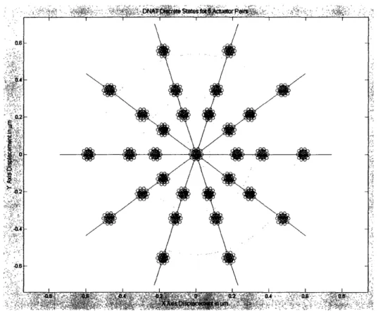
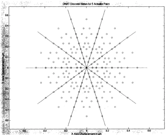
The ratio of the stiffnesses in the higher and lower stiffness flexures, respectively referred to as kH and kL, dictates the pattern and locations of the discrete states. There are three cases: 1) the two flexures are orders of magnitude apart as in Fig 2.3, 2) the two flexure stiffness approach each other as in Fig 2.4, and 3) the stiffnesses are equal as in Fig 2.5.
0= N. .4* ,~ 0 ' 2? .,I-.9. - . -G -1 4 - " , (s -1, v55 ,T~ - E ss tM A~r- -,,.g , W "f .- E \t vz> a o W:, .. -. . . .<, 'i - . I -r 7 ,.t .... a So t~~~~ ~ ¾Y ~~~~~~~~~~~~~~~~~~~~~~~~~~~~- .
Figure 2.3: Discrete state geography for a DNAT with five actuator pairs and kH >> kL
Figure 2.4: Discrete state geography for a DNAT with five actuator pairs and kH -- kL
f
05 04 t0 *011 44 46
DRA DST ceteti3s fo 5 Attmlor . ^ .
, .4 X .0
0
020.4
0.v
Figure 2.5: Discrete state geography for a DNAT with five actuator pairs and kH = kL
Figure 2.3 shows that in the case where the two stiffnesses are orders of magnitude apart, the discrete states appear as widely spaced tight clusters. For the DNAT to replace modem analog nanopositioners, it is clear that the ratio differential stiffnesses cannot approach this limit. When the stiffness of the two flexures are equal as shown in Fig 2.5, the states resemble an equally spaced "lattice" around the origin. This geography could be exceptionally useful for applications such as photonics, where fiber optic cables are often moved in a grid. Finally, in the case where the two stiffnesses approach each other as in Fig 2.4, the majority of the states are located within a large circle centered around the origin. For our purposes, this proves to be the most useful of the three cases, as the density of the states within that circle enables the DNAT to approach the performance of a continuous actuator. Adding more actuator pairs that are introduced allow the discrete position states of the DNAT to increases the density and thereby leads to finer resolution.
2.2 Flexure and actuator design
The flexure design was another important design consideration for the DNAT. The flexures must be easily fabricated using standard DRIE techniques, yet able to decouple error motions that result from to manufacturing errors and actuator misalignment. Figure 2.6 shows the final flexure designs, which were devised in order to have a symmetric flexure design to decouple error motions from actuator input.
l= _~~~~~~~~~~Hl
Figure 2.6: Flexure concept
The flexure is a combination of smaller "cells" arranged in series. This architecture allows the larger cells of the flexure to filter angular misalignment while allowing the cells closer to the actuator to remain in their original orientation. The flexure is also easily scaled to make it less compliant by simply increasing the cell width.
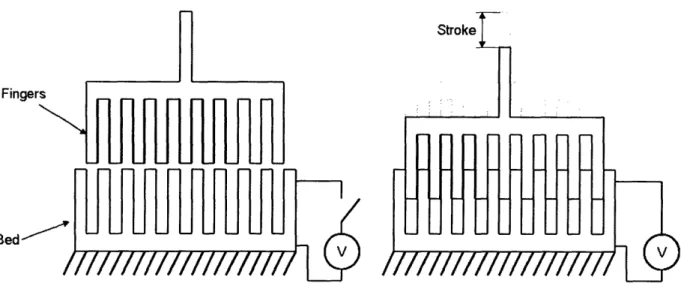
There are two well-developed methods of actuating MEMS devices: electrostatic comb drives and thermal actuators. In a standard electrostatic comb drive such as the one shown in Fig 2.7, interdigiated fingers of a flexible element are attracted by a force proportional to the voltage applied to the bed of the actuator.
Finger
Bed
Figure 2.7: Electrostatic comb drive
The force the actuator can exert is proportional to the number of fingers on the actuator and the square of the supplied potential. The force exerted is inversely proportional to the gap distance between the fingers. As a result, these actuators may provide high forces over small displacements, but they are incapable of producing the large displacements required for the DNAT's approximately 2 gm of actuator stroke.
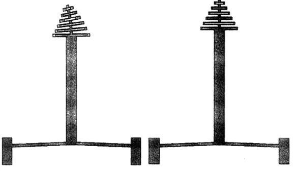
Thermal actuators operate based-upon on the thermal expansion of a material. When a voltage is applied to the material, it undergoes Ohmic resistance heating. The thermal strain induced by the material on the MEMS device provides the actuator stroke. As strain is directly proportional to voltage, this type of actuator is capable of providing a large displacement as well as substantial force. Often, two actuators are attached to the base of a chevron beam (the "v" shape at the bottom of the flexures in Fig 2.6). The chevron beam serves two purposes: 1) to amplify the displacement of the thermal actuators, and 2) to remove any misalignment of the actuators and provide motion in one degree-of-freedom. This improvement enables the effective use of thermal actuators in MEMS devices. As a result, the thermal actuator and chevron beam system was chosen for the DNAT device concept.
2.3 DNAT model
As described above in section 2.1, the DNAT is Cartesian nanopositioner accepts binary displacement inputs from actuators (6A, 8B, C, .. .) spaced evenly around the circumference of a central positioning stage. The ultimate goal for a model of the DNAT is to map the these actuator displacements to the displacement of the central positioning stage in the global coordinate system (, 8j) as shown in Fig 2.8.
Input
.
6
i -Si
d-
- I
Output
Figure 2.8: DNAT input to output flow
Figure 2.9 shows a diagram of a DNAT device with three actuator pairs which labels the different parameters used to fully describe the system.
Figure 2.9: DNAT terminology
E
,;,
Xt~sO
ft
\,w,
;
I
at'-Ah
"
enI
The actuators for the DNAT are labeled alphabetically in a counterclockwise direction. The actuator in the first quadrant of the i-j plane closest to 0 degrees is labeled A. The angle this actuator makes with the i-axis is A. Every actuator is connected to a flexure that has a stiffness
in the global coordinate system (ki , kj). The stiffness characteristics are derived from the flexural stiffnesses in the local coordinate system of the flexure, x-y. Each actuator also receives a displacement input at its end. This displacement input is either zero (OFF), or a finite number 6 (ON). Note that an actuator may never be in a state other than ON or OFF. The origin of the i-j coordinate system is defined at the center of the positioning stage when all the actuators
are in the OFF position.
As all actuators are spaced equally around the circumference of the device, it is possible to find the angle of any actuator, An (note that the subscript n refers to the numeric compliment of a letter, i.e. A=1, B=2, etc.), by knowing the total number of actuators, N, and the angle actuator A makes with the i-axis, OA. Equation 3 provides a means to calculate these angles:
= A (n - 1) 360 (3)
N
There are two different types of local stiffness matrices that are used in a DNAT device, one corresponding to the higher stiffness flexural members, which is defined in eqxn. 4, another to the lower stiffness members, which is expressed by eqxn. 5.
kx,havy 0 -kx,heavy 0
k~~heav
y
heavy
0k
y ,heav 0 y -0(4)-kyhea kheavy heavy ° - ky,heavy ° kyheavykxjigh l
klight = - kih,
x~ight
Figure 2.10 shows displacements of displacements define the stiffnesses in
o -kxlight
kylight 0
- kky, light 0
-k yighi 0
the flexures in the the local coordinate
0
-
kylight (5)0 (5)
k ylight
local x-y coordinate system. These system.
_
Y XI-a) x-displacement b) y-displacement
Figure 2.10: Flexure displacements in the local x-y coordinate system
In order to convert these local stiffnesses to global stiffnesses, it becomes necessary to define a transformation matrix, A, which transforms all local displacements and forces into the global frame for each actuator. This orthogonal rotation matrix is defined by eqxn. 6:
-cos OA -sin OA 0 0
A A= sin A cosA sA (6)
A 0 0 -COS A -sin
0
A0 0 sin OA cos OA
The conversion of the local stiffness matrices, k, to the global coordinate system, K, occurs via eqxn. 7.
K ATkA (7)
The next step in the analysis is to compute the global stiffness matrix, Kglobal, that links the forces at each node to the displacements at each node as shown in eqxn. 8.
F
FAi MaiF
-
Kglobal Aj(8)
F
FB
As each node has two degrees of freedom in the global coordinate system, it is necessary to convert the N global 4 x 4 stiffness matrices for each actuator into (2N+2) x (2N+2) matrices. Note that the center stage is considered a node, and therefore adds two degrees of freedom to the
system. By adding these N matrices together, the global stiffness matrix is constructed.
When the DNAT is in an equilibrium position corresponding to one of its discrete states, the forces at the center stage F and F will both be equal to zero. Equally important to acknowledge is that 4,i and 4,J can be found for each local actuator input by multiplying that actuators displacement, 4, by the cosine and sine respectively of the actuator angle, 0n. Combining this information reduces the number of equations needed to be solved in the matrix system of equations to the following:
j
= Kglobal ar , Si A COS A JA sin A 8B COS OB 8B sin OB J (9) I~~~Once eqxn. 9 is obtained, one may solve it via Gaussian elimination (there are two equations and two unknowns, 8i and 6j). A MATLAB® script based on the preceding theory has been created for simulating the discrete states of the DNAT and is included in Appendix A. For any P pairs of actuators, it accepts the local flexure stiffnesses and the actuator displacement inputs and then computes the output of the center stage for all 22P states.
Chapter 3
Fabrication
The fabrication of the DNAT prototype was carried out in the Microsystems Technology Laboratory (MTL) located on the grounds of MIT. The MTL houses three clean room facilities: the Integrated Circuits Laboratory (ICL), the Technology Research Laboratory (TRL), and the Nano-Structures Laboratory (NSL). The majority of the facilities for fabricating MEMS devices are located in the TRL and ICL.
The fabrication process for the DNAT was based on the micro-fabrication technology techniques commonly used in the mass production of integrated circuits. The entire device was fabricated on an SiO2 wafer with a 50 gm device layer. The process consists of five main steps that are illustrated in Fig 3.1.
1. Deposit a 1 gm aluminum actuator layer
2. Pattern the aluminum layer using aluminum etchant
3. Pattern the DNAT device structure with deep reactive ion etch (DRIE) 4. Etch the back side of the device with DRIE
Prime Wafer 1 \ 3 57 L 5 _ _ 2 4
Figure 3.1: DNAT fabrication process
3.1 Introduction to microfabrication
Before the fabrication process for the DNAT is revealed in detail, it is necessary to first give a brief introduction to microfabrication. The first step in fabricating a MEMS device is to choose a wafer to perform the microfabrication process on. The architecture of the DNAT suggests that a multi-layer wafer be used. One natural choice is a silicon on insulator (SOI) wafer, which has three layers. The first is a thick silicon handle layer which provides the substrate base for the device. The next layer is made of oxide, which provides a stop for the DRIE etching process. Finally, the top layer is the device layer, which is made of silicon and provides the substrate for the entire DNAT positioner.
Once a wafer is chosen, lithography and etching are used to produce the desired device architecture. Figure 3.2 provides the process flowchart and the six steps of the process.
Figure 3.2: Microfabrication process overview
Photolithography represents up to 50% of all time spent during fabrication. In this process, a wafer is first exposed to Hexamethyldisilazane (HMDS), a powerful chemical agent that dehydrates the surface of the wafer and allows the adhesion of the photoresist layer to the surface of the silicon wafer. Photoresist is then dynamically applied to the wafer by pouring in onto the center of the wafer, and then spinning it until the desired thickness of the photoresist is reached. The thickness of the photoresist layer is determined by both the viscosity of the solution and the rotational velocity of the wafer. The wafer is then pre-baked at 90°C to remove solvents that may be present in the photoresist and adversely affect the quality of the etch down the line. The next step is to expose the wafer to ultraviolet light. By using a pre-fabricated mask imprinted with the device geometry, the architecture of the device may be patterned onto the wafer as the areas the light shines on chemically alters the photoresist. The wafer is coated with hydroxide developer, and then rinsed and dried with a nitrogen gun, thus removing the undeveloped photoresist on the wafer. Finally, the entire wafer is baked at 120 °C which permits the photoresist to harden.
Lithography
Apply
||Expose
Post-Bake
Etching is the process by which the silicon device layer is shaped into the final device architecture. There are a few different types of etching processes that may be used on a post-baked wafer, but one extremely common process is DRIE. In deep reactive ion etching, the patterned wafer is bombarded with ions thus producing the desired geometry on the device layer. Once the ions reach the oxide layer, the etching process immediately finishes. DRIE is a desirable process for a few reasons. Most chemical and vapor etching methods are unable to produce wall angles of 90 degrees, but DRIE is able to achieve this with ease (most of the time within + 2). Furthermore, DRIE can achieve depth to width aspect ratios of 30:1, which is unheard of in chemical and vapor etching. With speeds of up to 10 gm/min during the etching process, DRIE is also able to leave finishes down to 10 nm on the etched walls. Once the DRIE process is finished, a similar etch is performed on the underside of the wafer to expose the oxide layer. The exposed oxide layer of the wafer is then bathed in hydrofluoric acid, referred to as a Buffered Oxide Etch or BOE, to remove the oxide layer, thus freeing the device layer from the oxide layer and allowing device motion.
The final microfabrication technique used during the production of the DNAT prototype is vapor deposition. In vapor deposition, a cleaned, cool wafer is placed in a high vacuum chamber. A crucible containing aluminum (or other metal) is heated with an electron beam until the aluminum evaporates. The superheated aluminum vapor comes into contact with the cool surface of the wafer and begins to condense. The result is an extremely even coating of aluminum on the surface of the wafer, bonded directly to the silicon substrate beneath it. Using an electron beam, this aluminum layer can be patterned to any desired planar geometry.
3.2 DNAT microfabrication process
The fabrication process for the DNAT prototype is quite straightforward and follows from the discussion in section 3.1:
1. Deposit a 1 gm aluminum actuator layer
2. Pattern the aluminum layer using an electron beam
3. Pattern the DNAT device structure with deep reactive ion etch (DRIE) 4. Etch the back side of the device with DRIE
5. Release the device with BOE (etch rate approximately2.3 gm/min)
6. Clean device with acetone bath and oxygen
The detailed process and fabrication description of the final DNAT prototype is presented in Table 3.1.
Table 3.1: DNAT fabrication process [6]
Step Lab Machine/coral Recipe/description
ICL RCA Hood Starting with 6" SOI1 wafer. Device ,,, ... layer = 50 gm. Oxide layer = 2 gm.
Handle layer = 500 gm.
- - - ICL Endura Deposit 1 micron Al+2%Si and
ITRL
Coater/Prebake/EV1/ pattern the Al in TRL. (Etch Al with_Photowet/Postbake
Aluminum etchant.) TRL Acid HoodTRL Coater/Prebake/EV1/ Apply and pattern the photoresist for Photowet/Postbake DRIE.
rim
TRL STS 2 Pattern the structure with DRIE. l~ l l l l/~
[ 1 F
| TRL Asher Remove the photoresist and clean3.3 DNAT microfabrication quality
The patterning of the photoresist during the lithography process is crucial to maintaining the desired device geometry (and thus the desired stiffnesses) for the DNAT flexures. If these flexures are not patterned correctly onto the photoresist, none of the discrete states will be in their predicted locations. There are only a few variables which can affect the resolution and the patterned geometry during the photolithography process, and they are the exposure time and type of photoresist.
Exposure time refers to the time that the ultraviolet light source is allowed to shine through the mask onto the photoresist covered wafer. In a perfect exposure such as the one shown in Fig 3.3, the mask completely preserves the geometry onto the photoresist. The edges are completely crisp and well defined. If the exposure time is significantly increased, the light
TRL Coater/ Pre-bake Spray coat photoresist onto SOI
_I_________________Oven wafer. Wafer-mount the SOI to a
transparent quartz wafer.
TRL Coater/Prebake/EV1/ Spin on and pattern the photoresist Photowet/Postbake onto the handle wafer.
I :
TRL STS 2 Pattern the handle wafer with DRIE.
TRL Acid Hood Remove the oxide layer through
_ _ _ _ _ _ _ _ _ _ _ _ _ _ _ B O E .
TRL Photowet Separate the SOI wafer from quartz
I [L [J ] wafer in acetone bath for 24 hours.
L
J L J
~~~Asher L Clean the final device in oxygen plasma asher. Process finished.begins to diffract and the photoresist begins to modulate in the areas protected by the photoresist. As a result the patterned wafer will lose definition, and features will tend to be much larger than they were actually intended to be. In the case that the wafer was underexposed to the light source, the photoresist will not have been modulated enough, and as a result, the features will be much smaller than they were originally designed to be. There is no formula or rule for determining exposure time, so care should be taken to experiment with different exposure times and evaluate which times produce the best results in terms of both device resolution and accuracy.
Besides exposure time, the type of photoresist chosen will dramatically change the resolution and accuracy of the final device. From the previous discussion on exposure time, one can see that if the photoresist layer was very thin, the process would be less susceptible to error from improper exposure time. The realization that thin photoresist generally has higher resolution than thick photoresist leads to a good rule of thumb for choosing a photoresist for a particular application. For example, the positive thin photoresist OCG 825 was used in the production of the DNAT prototype due to its ability to easily attain sub-micron resolution. In contrast, a 10 gm photoresist would be lucky to achieve a working resolution of one micron.
Light Mask
<ilillL| | | |111!111 lPhotoresist
11111 g7
?
Over Exposure Ideal Exposure Time Under Exposure
Figure 3.3: Effect of Exposure Time on Photoresist Pattern
-////////
r I l,10 0 i 0,.1lil i I 0 ~ 1,iFiF1Chapter 4
Results and analysis
A prototype DNAT device (see Fig 4.1) with three actuator pairs was fabricated in the MTL. The device measures roughly 12 mm in diameter, with the smallest features on the flexures being roughly 35 microns wide. The thermal actuators are each roughly 0.5 mm2 in footprint.
Figure 4.1: DNAT prototype solid model
4.1 Theoretical results
The MATLAB analysis program developed from the model presented in section 2.3 needs two things in order to complete its predictions for the center stage displacement of the
DNAT prototype: the local stiffnesses of the higher stiffness and lower stiffness flexures, and the displacement input for each actuator. The local stiffnesses of the flexures are easily found by taking the solid model of the DNAT device and running a statics simulation with a standard FEA package such as COSMOSWorks©. The results of the simulation are presented in Table 4.1:
Table 4.1: Simulation results for local stiffnesses
Higher Stiffness Flexure Lower Stiffness Flexure
X- Stiffness (N/m) Y- Stiffness (N/m) X- Stiffness (N/m) Y- Stiffness (N/m)
70360 36200 1152 35910
Using the thermal analysis software included in the COSMOSWorks© analysis suite, 3.0 V was applied to each of the actuators on the chevron beam actuators. The actuator displacement was found to be 1.5 gm from the simulation.
Using these values as inputs to the analysis program written specifically for DNAT, the prototype was found to have 49 unique states with an overall range of 1.272 gm. The smallest discrete state was 31.6 nm away from the origin. The discrete states appear in seven clusters of seven evenly spaced states. One of the clusters is centered about the origin, while the other six are evenly spaced around the circumference of the device at a distance of 605 nm from the origin. Figure 4.2 is the output from the MATLAB® simulation showing the location of each discrete state in the global Cartesian coordinate system. The global displacements for each discrete state as predicted by the MATLAB script are presented in Appendix B.
Figure 4.2: DNAT prototype predicted discrete states
4.2 Experimental setup
Once the DNAT prototype was removed from the fabrication facilities located at the MTL, the wafer was die cut into 1 inch squares and placed into a specially made adaptor board shown in Fig 4.3 that was mounted to a block of Delrin. Using a wire bonding machine, each actuator was connected to a solder pad on the adaptor board with gold wire.
1"
.
1< ;
I
Figure 4.3: DNAT prototype attached to adaptor board
Motion data for the DNAT prototype was acquired through the use of a UMECH Technologies MMA G2 MEMS Motion AnalyzerM unit. The system pictured in Fig 4.4 consists
of a microscope outfitted with a high resolution camera and a strobe flash.
The system outputs a sinusoidal driving voltage to the DNAT prototype, producing an oscillatory center stage movement in the device. The system then flashes a strobe light under the microscope objective, allowing the camera (1240 x 1024 resolution) to take still photographs of the motion in rapid succession. The computer software than analyzes the still motion capture images and outputs the in-plane motion of the center stage by tracking regions of interest (edges and discolorations) of the center stage of the device. The MMA G2 specifications are listed in Table 4.2.
Table 4.2: MMA G2 system image capture specifications
5x Objective 20x Objective
NA 0.13 0.4
Resolution 40 nm 10 nm
X Field of View 1.6 mm 0.5 mm
Y Field of View 1.2 mm 0.4 mm
Max Tilt Angle Motion Range + 2.5 deg ± 10 deg
The waveform generator for the MMA G2 was cable of outputting a 1 Hz to 10 MHz sine wave at + 10 V and 10 mA. The data acquisition board had a 10 bit resolution with a 40 MHz sampling rate.
The DNAT prototype was mounted to the microscope unit using double stick tape. The wires from the device to the MMA G2 were sufficiently strain relieved prior to testing. The prototype was then driven with a 10 Hz sine wave measuring 3.00 V peak to peak. 10 seconds of motion was captured and analyzed to determine the resulting motion for each discrete state. The
entire device was then subjected to a 0 Hz to 5 kHz frequency response. The data for each was then recorded and saved in MATLAB® for post processing.
4.3 Experimental results
Due to scheduling conflicts and machine maintenance, a full set of motion data could not be obtained for each discrete state of the DNAT prototype. At the time of publication, only data corresponding to thirty of the forty-nine unique states had been collected. This data is sufficient enough, however, to validate the accuracy of the model. The experimental results are presented in Fig. 4.5.
Figure 4.6 overlays the experimental data onto the theoretical predictions. It becomes apparent that the general model shape is correct: a set of six clusters spaced radially around the origin, with one extra cluster centered at the origin.
Figure 4.6: DNAT prototype experimental and theoretical results
While the experimentally determined locations for the discrete states do not exactly mirror the theoretical predictions, it is possible to explain these deviations. The reason the data points in each cluster are spaced further apart from each other than the tight clusters that the computer simulation predicted has to do with a manufacturing error in the prototype DNAT. The mask used to fabricate the DNAT was hand made and not obtained commercially. This mask
has a resolution of 15 gm, which is 42% the size of the smallest feature (35 gm) on the flexures. This limited resolution has a huge effect on the overall stiffnesses of the beams, which depend on the moment of inertia of a square cross section. Since the moment of inertia depends on the height of the beam cubed, this means the stiffness could change by a factor of three from the original design due to the mask resolution. This would dramatically alter the locations of the outer clusters and the spacing of the states in each cluster.
Another reason for the discrepancy is due to the quality of the fabrication steps used in the production of the final DNAT prototype. Figure 4.7 shows an actual photograph taken of the flexures on the prototype DNAT. The picture details an area of the flexure where the definition of the structure was lost, and the two compliant links which should have been independent were actually connected by a silicon bridge that should have been removed during the etching process.
Figure 4.7: DNAT prototype flexure defects
Defects such as this will undoubtedly change the overall local stiffness of the flexure, and this will have a huge impact on the location of the final discrete states.
Another important detail concerns the deformation of the chevron beam actuators. The design of the flexures do not completely decouple the center stage motion from the chevron beam. As a result, when the center stage beams move, the chevron beams of all six actuators
stretch and deform. However, some of these chevron beams are already deformed because the actuators attached to them are in the ON position. This means that the beams will undergo different rates of strain stiffening (strain stiffening can dramatically increase the stiffness of a flexure). This would explain why on the x-axis the cluster to the very right has a wide distribution of states (this cluster is opposite a higher stiffness flexure), while the leftmost cluster on the x-axis has a very tight distribution (this is opposite a lower stiffness flexure).
Finally the clusters do not seem to be spaced evenly around the circumference as the model predicted. This means that the device is not symmetric as the original solid models intended them to be. As a result the model, which does not take into account an actuator's angular position error, will deviate significantly from the experimental data when the actuator/flexure pairs are not placed evenly around the center stage.
The frequency response data was also very interesting for the DNAT device. Figure 4.8 shows the frequency response of the device in the x-direction. The device shows a usable bandwidth of approximately 0-50 Hz. This makes sense as the thermal actuators need time to cool off and go back to their normal size before they can have voltage applied to them again and grow to their full ON stroke dimension. Figure 4.9 is the frequency response data for the y-direction, and it confirms the same results found in the Fig 4.8.
10
Figure 4.8: DNAT prototype X axis frequency response
1 0.1 0.01 0.001 0.0001 Frequency (Hz)
Phase Angle
200 150 100 (0 50 0 50 · - 0 L.0 O1a
-50
-100 -150 -200 Frequency (Hz)Figure 4.9: DNAT prototype Y axis frequency response
Mannitid
1- I v '-I' 0.1 -0.01 0.001 -0 N0001 -00 Frequency (Hz) .- I l T I)
1000 2000 3000 4000 5000 60 % 4~~~~~~~~~~~~~~ 4200
150 100 )50
50 0 0 a -50 -100 -150 -200 Frequency (Hz)Chapter 5
Conclusion
5.1 Summary
This thesis presented a new type of Cartesian MEMS nanopositioner that requires no sensing or feedback control. The MEMS device, which utilized discrete nano-actuation technology (and therefore referred to as DNAT), was digitally actuated by a set of chevron beam thermal actuators. These actuators were placed around a central stage in diametrically opposed pairs of light and heavy actuators. The DNAT prototype was capable of accurately achieving
submicron level motion without the need for sensing and controls.
This thesis takes the concept proposed by Culpepper and Chen [5] and augments it in the following:
1. Creation of a modeling technique for the DNAT. Before this thesis was published, there was no model for a DNAT device in existence that would give the locations of all the discrete states for a device with P pairs of actuators. This thesis created a modeling technique that uses the number of actuator pairs, the local stiffnesses of the light and heavy flexures, and an actuator displacement input to predict the performance of a DNAT nanopositioner. This modeling technique empowers the precision engineer with the tools necessary to design a DNAT nanopositioner to meet his/her particular design requirements.
2. Design considerations such as actuators and flexures were discussed. Crucial steps in designing the DNAT prototype such as flexure choice/design as well as
actuator choice were presented in this publication. The thesis document gives a precision engineer enough exposure to both of these topics to make knowledgeable decisions in the design and implementation of a DNAT actuator.
3. A discussion of microfabrication and how it plays a role in DNAT design. This thesis outlined the main steps of microfabrication, giving precision engineers unfamiliar with the process enough knowledge to make intelligent decisions regarding DNAT architecture. Furthermore, errors in the microfabrication process resulting in diminished device resolution were identified and ways to mitigate these errors were presented.
4. A DNAT positioner prototype was created and tested. The prototype device verified the modeling techniques presented earlier in this thesis document. Discrepancy between the experimental results and model were discussed in detail. Furthermore, the experimental results gave rise to new design considerations, all of which add to the knowledge base that the precision engineer has to work off of when designing these types of digitally actuated micropositioners.
The results of the prototype DNAT are not meant to provide absolute metrics of performance for the device. Instead, it was meant to provide the proof of a concept and the verification of a modeling methodology. This prototype has created a new class of positioner that has never been explored at the MEMS level. The experimental data has provided many new design considerations and opened up many new avenues for future research.
5.2 Future work
Many new questions have emerged from the work published in this thesis document. The prototype device fabricated for this research project was patterned from a mask with very poor resolution. In a device with much higher resolution, how do slight stiffness errors in the device architecture effect the accuracy of the device? The device prototyped for this publication was not able to be used to predict system tolerance to stiffness variations in a high quality production DNAT. Is there an easy way to map these errors due to stiffness variation? Furthermore, is there a way to design the flexures such that they will not be susceptible to any of the effects of strain hardening? If not, is there a way to add these effects of strain hardening to the model, thus allowing the model to more accurately predict the actual device's performance? Finally, implementation of one of these devices as a fine motion positioner in conjunction with a coarse six axis positioner such as a Stewart Platform should be planned in order to verify the open loop positioning system as a whole.
References
[1] Image reproduced with permission from Physik Instrumente online catalog (http://www.physikinstrumente.com)
[2] Image reproduced with permission from Physik Instrumente online catalog (http://www.physikinstrumente.com)
[3] Image reproduced with permission from PCS website (http://psdam.mit.edu)
[4] Mukherjee, S. and Murlidhar, S., "Massively Parallel Binary Positioners," Transactions of the ASME, Vol. 123, March 2001.
[5] Culpepper, M. L. and Chen, S.C., "Modeling and Design of Digitally Actuated Compliant Nano-positioners," Submitted to Precision Engineering, in revision.
Appendix A
DNAT analysis script (written for use in MATLAB®)
This MATLAB® script was written to reflect the theory outlined in section 2.3. It takes in the number of actuator pairs, the local stiffnesses for the heavier stiffness and lighter stiffness flexures, the angle the first actuator makes with the global x-axis, and the thermal actuator displacement input. It outputs a global stiffness matrix for the device and the global displacements for each of the 22P discrete states. Finally, the script also displays the usable states in a Cartesian global x-y plot.
%This script creates the global stiffness matrix for a DNAT with p pairs of actuators and %computes the global displacements of the center stage
function [Kglobal,dispglobal] = DNAT
%DNAT nodes are as follows for a 3 pair example: % C B
% \ /
% D-G-A
% / \ % E F
%Node A is 3,4 in global displacement %Node B is 5,6 in global displacement %Node C is 7,8 in global displacement %Node D is 9,10 in global displacement %Node E is 11,12 in global displacement %Node F is 13,14 in global displacement %Node G is 1,2 in global displacement %Accepting user input for DNAT definition
prompt = { 'Number of Actuator Pairs:','X-Direction Stiffness for Stiff Beam (N/m):','X-Direction Stiffness for Compliant Beam (N/m):','Y-Direction Stiffness for Stiff Beam (N/m):','Y-Direction Stiffness for Compliant Beam
(N/m):','Angle of First Actuator with X-Axis (Degrees):','Actuator Displacement Input (Microns):'}; title ='DNAT Device Definitions';
lines= 1;
def = {'3','171.4','3271','1501','468.8','0','1.5'}; answer = inputdlg(prompt,title,lines,def);
%Converting all inputs from string to numbers p=str2num(answer{ 1 });
k_x_heavy=str2num(answer {2}); k_x_light=str2num(answer 3 }); kyheavy=str2num(answer 4 }));
theta_A=str2num(answer 6 }); d_end=str2num(answer 7 });
%N is number of actuators N=2*p;
%Making a column vector of actuator displacements in meters d_actuators= 1E-6*d_end*ones(N, 1);
%Calculate global angles for all N DNAT beams in radians theta=zeros(N, 1);
for i=l:l:N
theta(i, 1)=(pi/1 80)*(thetaA+(i-1 )*(360/N)); end
%Next step is to find the local stiffness matrix for each beam
k_localheavy=[k xheavy 0 -kxheavy 0;0 kyheavy 0 -kyheavy; -kx heavy 0 k-x-heavy 0;0 -kyheavy 0 kyheavy];
k_locallight=[kxlight 0 -kxlight 0;0 kylight 0 -kylight; -k_xlight 0 kxlight 0;0 -kylight 0 kylight];
%Now must make a coordinate transformation matrix for each beam A=cell(N, 1);
for i=l:l:N
A{i}=[-cos(theta(i, 1)) -sin(theta(i, 1)) 0 0; sin(theta(i, 1)) -cos(theta(i, 1)) 0 0; 0 0 -cos(theta(i,1)) -sin(theta(i,1)); 0 0 sin(theta(i, 1)) -cos(theta(i, 1))];
end
%Calculating the local stiffness matrices (4x4) k=cell(N, 1); for i=1:l :N index=(-1)^i; if index == -1 k{ i }=(transpose(A i}))*klocal_heavy*A{ i }; else k{ i } =(transpose(A{ i } ))*klocallight*A { i }; end end
%Intializing the local stiffness matrices in the global matrix form (N+2 x N+2 instead of 4x4) k_e=cell(N, 1);
for i=1 :1 :N
ke { i } =zeros(2*N+2,2*N+2); end
%Converting 4x4 local matrices to global matrices for i=1:l:N
temp=k i };
tempglobal=ke i };
tempglobal(l +2*i, 1 +2*i)=temp(1,1); tempglobal( 1 +2*i,2+2*i)=temp( 1,2); tempglobal(I +2*i, 1)=temp(1,3); tempglobal(1 +2*i,2)=temp(1,4); temp-global(2+2*i, 1 +2*i)=temp(2, 1); tempglobal(2+2*i,2+2*i)=temp(2,2); tempglobal(2+2*i, 1 )=temp(2,3);
tempglobal(2+2*i,2)=temp(2,4); tempglobal( 1,1 I +2*i)=temp(3, 1); tempglobal(l 1,2+2*i)=temp(3,2); tempglobal( , I1 )=temp(3,3); tempglobal( 1 ,2)=temp(3,4); tempglobal(2,1 +2*i)=temp(4, 1); tempglobal(2,2+2*i)=temp(4,2); tempglobal(2, 1 )=temp(4,3); temp_global(2,2)=temp(4,4); ke{ i }=tempglobal; end
%Computing the global stiffness matrix from beam global matrices Kglobal=zeros(2*N+2,2*N+2);
for i= 1:l :N
K_global=Kglobal+ke i }; end
%The 2 x N+2 stiffness matrix that allows us to find the displacements at the center K_center=[Kglobal( 1,:);Kglobal(2,:)];
%sn x N matrix with all the discrete states possible in an N arm DNAT. %Column =A, Column 2=B, etc
for i=O: :(2^N) -tempstring=dec2bin(i,N); temp=[tempstring(1,)' ']; for j=2: :N temp=[temp tempstring(l ,j) ]; end states(i+ ,:)=str2num(temp); end s_n=size(states, 1 );
%Makes the first N columns of dispglobal equal states (allows for searching in Excel) %Then the next two columns will be x and y coords
dispglobal=states;
%Now to perform elimination on K_center multiplier=Kcenter(2,1 )/Kcenter( 1,1);
K_center(2,:)=Kcenter(2,:)-multiplier*Kcenter( 1,:);
%Now to calculate dj for every possible state, and put it in the N+2 column of dispglobal %Initializing the off on matrix, which puts the local displacments either off or on
offon=zeros(sn,N); for i=1:l:N
offon(:,i)=states(:,i)*dactuators(i, 1); end
%Initializing the displacements matrix, which has the global displacements except for the center stage displacements=zeros(2*N,s_n);
%Calculating the displacements in global coords for i=l:l:s_n
for j=2:2:2*N
displacements(j- I ,i)=[offon(i,j/2)*cos(theta(j/2, 1))]; displacements(j,i)=[offon(i,j/2)*sin(theta(j/2,1 ))]; end
end
dj=(-K_center(2,3:(2*N+2))*displacements)./Kcenter(2,2); dispglobal(:,N+2)=transpose(dj);
%Now to compute d_i
displacements(2:(2*N+l ),:)=displacements; displacements( 1,:)=dj;
d_i=(-Kcenter(1,2:(2*N+2))*displacements)./K_center( ,1); disp_global(:,N+l )=transpose(di);
%Graphing the output states m_i=max(d_i); mj=max(dj); if m_i>=mj scale=(m_i/l e-6); else scale=(mj/le-6); end
plot(transpose(d_i)/l e-6,transpose(dj)/1 e-6,'bo')
set(gcf,'Name', 'DNAT Motion Analysis','NumberTitle','off); axis([-1.2*scale 1.2*scale-1.2*scale 1.2*scale])
axis equal
Title(['DNAT Discrete States for' num2str(p) ' Actuator Pairs']) xlabel('X Axis Displacement in {\mu}m')
ylabel('Y Axis Displacement in {\mu}m') for i=l :1 :p
line([- 1.2*scale*cos(theta(i, 1)); 1.2*scale*cos(theta(i, 1 ))],[- 1.2*scale*sin(theta(i, 1)); scale*l .2*sin(theta(i,1))],'Color',[0,0,0]);
end
rectangle 1 =rectangle('Position', [-0.125
*scale,-0.125*scale,0.25*scale,0.25*scale],'Curvature',[ 1, l],'EdgeColor',[0.7,0.7,0.7]);
rectangle2=rectangle('Position',[-0.5*scale,-0.5*scale,scale,scale],'Curvature',[ 1,1 ],'EdgeColor',[0.7,0.7,0.7]);
rectangle3=rectangle('Position',[-0.875*scale,-0.875*scale, 1.75*scale, 1.75*scale],'Curvature',[ 1, 1],'EdgeColor',[0.7,0.7,0.7]); range=2*scale;
V=axis;
if round(p/2) == (p/2) usable=3Ap; else
usable=(2 AN)-2*(2 Ap)+ 1; end
Appendix B
DNAT experimental/theoretical data
This appendix contains the x and y global positions of the discrete states as determined experimentally from MMA G2 MEMS Motion Analyzer as well as theoretically from the MATLAB script presented in Appendix A.1. The first 6 columns of each of the following tables represent the ON (1) and OFF (0) commands given to each actuator.
Table B.I: Theoretical data
Actuator 1 Actuator 2 Actuator 3 Actuator 4 Actuator 5 Actuator 6 X[um] Y[um]
0 0 0 0 0 0 0.00 0.00 0 0 0 0 0 1 0.30 -0.52 0 0 0 0 1 0 -0.02 -0.03 0 0 0 0 1 1 0.29 -0.55 0 0 0 1 0 0 -0.60 0.00 0 0 0 1 0 1 -0.30 -0.52 0 0 0 1 1 0 -0.62 -0.03 0 0 0 1 1 I1 -0.32 -0.55 0 0 1 0 0 0 -0.02 0.03 0 0 1 0 0 1 0.29 -0.50 0 0 1 0 1 0 -0.03 0.00
.~~~~~~
0 0 1 0 1 1 0.27 -0.52 0 0 1 1 0 0 -0.62 0.03 -__ - -o1 0 1 0 1 :0.32 -0.50 0 0 1 1 1 0 -0.64 0.00 o~i~ 0 1 11 1 -0.33 -0.52 0 1 0 0 0 0 0.30 0.52 o V 0 0 0 1 0.60 0.00 0 1 0 0 1 0 0.29 0.50 0 I 0 0 1 0.59 -0.03 0 , 1 0 1 0 0 -0.30 0.52 0 ,1 0 1 0 1 0.00 0.00 0 1 0 1 1 0 -0.32 0.50 0 1 0 1 1 1 -0.02 -0.03 0 1 1 0 0 0 0.29 0.55 o I 0 0 1 0.59 0.03 0 _ i 1- o o 1~~0 0.59 0.030.27 0 0 o 0 1 1 1 1 1 1 1 1' 1 1 1 1 1 1 1 1 1 i 1 1 1 1 1 ! 1 ' 1 1 - :''-'-1 0 0 =0: 0 0 0 0 0 0 .... O : 0 0
0'
-. o 0 1 1 1 1 1 1 1 . . / - 0 ' 1 - - .1 1 1 1 1 1 :".", o'11 1 0 0 0 0 0 1 1 1 1 1 1 1 0 0 0 0 1 1 - . ': '_'I
1 1 -1 ' ' O 1 1 i 0 / 0 "m0 0 1 · ~ ~1: 1 1/ 0 o 0 ' ' 0 0 1 ~~~~~~~~~~~~~~-'1 . -. . ,' -.1: 0 o: 0 ' 0 0 1 1 11 1 . 1--1 1 0 1 1 0''0
1 ., , !'-1 0 ' 01 0 _"''" 01 0 '. "'. O-1 1 0 1 0 1 0 11 "'' 1 1 0 1 0 0 1 0 0 . 1. 0 1 0 - .1 0 '1 01 0 0 . .. i 01 0 . 1 0 -. 1 0 . -. ~1 0 ....~~~ 0.57 -0.32 -0.02 -0.33 -0.03 0.03 0.33 0.02 0.32 -0.57 -0.27 -0.59 -0.29 0.02 0.32 0.00 0.30 -0.59 -0.29--0.60 -0.30 0.33 0.64 0.32 0.62 -0.27 0.03 -0.29 0.02 0.32 0.62 0.30 0.60 -0.29 0.02 -0.30 0.00 0.00 0.55 0.03 0.52 0.00 0.00 -0.52 -0.03 -0.55 0.00 -0.52 -0.03 -0.55 0.03 -0.50 0.00 -0.52 0.03 -0.50 0.00 -0.52 0.52 0.00 0.50 -0.03 0.52 0.00 0.50 -0.03 0.55 0.03-, 0.52 ::0.00 0.55 0.03 0.52 .0.00 0.52 0 1 1 0 1 0Table B.2: Experimental data
Actuator 1 Actuator 2 Actuator 3 Actuator 4 Actuator 5 Actuator 6 X[um] Yum]
0 0 0 0 0 0 0 0 1 0 0 0 0 0 -0.31 0.38 0 1 0 0 0 0 -0.08 0.01 0 0 1 0 0 0 -0.35 -0.5 0 0 0 1 0 0 0.07 -0.08 0 0 0 0 1 0 0.59 -0.01 0 0 0 0 0 1 0.05 0.07 1 0 0 0 0 -0.42 0.37 1 0 1 0 0 0 -0.72 -0.04 1 0 0 1 0 0 -0.27 0.32 1 0 0 0 1 0 0.38 0.35 1 0 0 0 0 1 -0.28 0.46 0 1 1 0 0 0 -0.5 -0.61 0 1 0 1 0 0 -0.07 -0.04 0 1 0 0 1 0.47 -0.01 0 1 0 0 0 1 -0.04 0.06 0 0 1 1 0 0 -0.33 -0.61 0 0 1 0 1 0 0.33 -0.57 0 0 1 0 0 1 -0.33 -0.48 0 0 0 1 1 0 0.61 -0.09 0 0 0 1 0 1 0.11 0.01 0 0 0 0 1 1 0.6 0.02 1 1 1 0 0 0 -0.81 0.03 1 0 1 1 0 0 -0.71 -0.02 1 0 1 0 0 1 -0.73 0.02 0 1 0 1 1 0 0.53 -0.06 0 1 0 0 1 1 0.54 0.05 0 0 0 1 1 1 0.65 0.01 1 0 1 0 0 1 -0.73 0.02 1 0 1 0 1 -0.65 -0.02 1 1 1 0 0 1 -0.79 0.01 1 1 1 1 0 0 -0.83 -0.01
![Figure 1.1: Current generation nanopositioner [ 1 ]](https://thumb-eu.123doks.com/thumbv2/123doknet/14684080.559853/14.933.284.641.114.410/figure-current-generation-nanopositioner.webp)
![Figure 1.3: Micro-HexFlex six degree-of-freedom micropositioner [3]](https://thumb-eu.123doks.com/thumbv2/123doknet/14684080.559853/15.933.278.649.435.792/figure-micro-hexflex-six-degree-of-freedom-micropositioner.webp)