Design and Analysis of a 6/4-GHz Receiver Front End
by Feikai Sheu
B.S. Elec. Eng., Massachusetts Institute of Technology (1994)
Submitted to the
DEPARTMENT OF ELECTRICAL ENGINEERING AND COMPUTER SCIENCE in Partial Fulfillment of the Requirements for the Degree of
MASTER OF SCIENCE IN ELECTRICAL ENGINEERING AND COMPUTER SCIENCE at the
MASSACHUSETTS INSTITUTE OF TECHNOLOGY May 1995
© Feikai Sheu, 1995 All rights reserved
The author hereby grants to MIT the permission to reproduce and to distribute copies of this thesis in whole or in part.
Author ...••... ... Department of Electrical Engineering and Computer Science
May 19, 1995
C ertified by ... ... ... ... .... ... ... ...
Professor David . Staelin Tesis Supervisor (Academic)
Certified by ... Jr•... Dr. RamesW K. Gupta Cq any Sup r (COMSAT Laboratories)
A rf•~rt hd ... ... MASSACHU OF TECHNJOLOGY
JUL 171995
UBRARIESBarker Eng
Design and Analysis of a 6/4-GHz Receiver Front End
byFeikai Sheu
Submitted to the
Department of Electrical Engineering and Computer Science on May 19, 1995
in Partial Fulfillment of the Requirements for the Degree of Master of Science in Electrical Engineering
ABSTRACT
This thesis presents the design and analysis of a miniaturized receiver front end for C-band satellite application. The use of monolithic microwave integrated circuit (MMIC) tech-niques, promises significant savings in mass and volume over current flight hardware. The receiver system is analyzed in terms of its prescribed performance requirements. Particular attention is placed on the downconversion unit, in order to establish component specifications which will enable compliance with the receiver spurious requirements. Based on the estab-lished component specifications, a local oscillator is designed. Several possible realizations are investigated, including phase-locked loop and multiplier chain. The multiplier chain ap-proach is selected for advantages of performance, reliability, power consumption, and size. Reference frequency in the local oscillator chain is provided by a low-noise, low-power tem-perature compensated crystal oscillator. Comb generation is achieved using MMIC silicon amplifiers with bias and drive levels adjusted for best performance. Several filter technolo-gies are considered, including surface acoustic wave, microstrip coupled-line, microstrip in-terdigital, and dielectric blocks. The driver stage is implemented with an MMIC gain block. Computer simulations are performed and breadboard is constructed to illustrate the local os-cillator design concept. The experimental local osos-cillator is then evaluated against design per-formance goals as well as simulation results. The successful breadboard prototype is
compli-ant with all performance specifications.
Thesis Supervisors: Prof. David H. Staelin
Department of Electrical Engineering and Computer Science Dr. Ramesh K. Gupta
Manager, Satellite and Systems Technology Division
Acknowledgments
This thesis would not have been possible without the support and help from many people. My sincere gratitude to Dr. Ramesh K. Gupta for recommendation of the topic as well as his supervision and the valuable guidance he has provided during the course of my stay at COMSAT Laboratories, both project-related and otherwise. I am also thankful to Professor David H. Staelin for his guidance and constant support.
Special thanks to George Estep for playing a crucial role in the successful completion of this project. His mentorship on engineering design, guidance on practical engineering is-sues, and illustration of the amusing side of engineering life have been inspiring, to say the least. I am indebted to Lou Pryor for timely and expert assembly of circuits for the bread-boarding efforts. Thanks also to Jim Buzzelli for his tremendous help on the bench. More special thanks to Dr. John Upshur for much friendly design assistance and Dr. Rene Bonetti for valuable lessons on filter design. To other members of the Microwave Components Department as well as other staff of COMSAT Laboratories, I sincerely express my appre-ciation.
I would like to thank COMSAT Corporation for funding this project, and Massachusetts Institute of Technology for the invaluable engineering internship opportunity.
To all my friends who have seen me through this project, I would like to express my gratitude. Last but not the least, I would like to thank all the members of my family - for without them I would never have made it this far.
Contents
1 Introduction ... 17
1. 1 Background and M otivation ... 17
1.2 M iniaturized Receiver Front End ... ... ... 20
1.3 Organization of Thesis ... 22
2 Front End Analysis ... ... ... 23
2.1 Introduction ... ... 23
2.2 System Perform ance Criteria ... 24
2.3 System Analysis ... 26
2.3.1 Initial System Design ... 27
2.3.2 Confirmation of Initial System Design ... .... 29
3 M ixer Spurious A nalysis ... 31
3.1 Introduction ... 31
3.2 M ixer Perform ance Criteria ... ... 32
3.3 Local O scillator Power Analysis ... 34
3.4 IF Filtering Analysis ... 35
3.5 Alternate M ixer Im plem entations ... .... ... 38
4 D esign of Local O scillator ... ... 39
4.1 Introduction ... ... 39
4.2 Local Oscillator Performance Criteria ... ... 39
4.3 Design Alternatives ... 42
4.3.1 VCO-based Phase-Locked Loop ... ... 42
4.3.3 Multiplier Chain... 51
4.3.4 Selection of Approach ... 54
4.4 Multiplier Chain Block Diagram Design ... ... 57
4.4.1 Frequency Multiplication... 58
4.4.2 Internal Interfacing ... 61
4.5 Selection of Signal Source ... 62
4.6 Implementation of Comb Generators ... 65
4.6.1 Selection of Comb Generation Approach ... 65
4.6.2 Operating Point Selection ... 67
4.6.3 Power Supply Filtering Circuits ... 73
4.7 Filtering ... 79
4.7.1 Specifying Filter Requirements ... ... 80
4.7.2 Surface Acoustic Wave (SAW) Filters ... .. 88
4.7.3 Microstrip Coupled-Line Filters ... 89
4.7.4 Microstrip Interdigital Filters ... .92
4.7.5 Dielectric Block Filters ... 96
4.7.6 Filter Selection ... 98
4.8 Driver Stage ... 98
4.9 Simulation ... 100
5 LO Implementation and Measured Results... ... 103
5.1 Introduction ... 103
5.2 Breadboard ... 103
5.3 Results ... ... 105
5.4 Comparison with Initial Specifications ... ... 111
6 Summary and Conclusions ... ... 113
A IF Filtering Requirement Analysis ... 117
B LO Filtering Requirement Analysis ... 119
B.1 Measured First-Stage Harmonic Spectrum Levels ... . 119
B.2 Predicted Second-Stage Harmonic Combs ... 120
B.3 Second-Stage Filter Specification ... 127
C Calculation of Minimum Filter Order ... ... 129
D Interdigital Filter Design ... 131
List of Figures
Figure 1.1 Block Diagram of Communications Transponder ... 21
Figure 2.1 Satellite Receiver Blocks ... ... ... 23
Figure 2.2 Block Diagram of Front End ... ... 23
Figure 2.3 Block Diagram of Gain Block ... ... 24
Figure 2.4 Design of Front End ... 27
Figure 2.5 Design of Gain Block ... ... ... 28
Figure 3.1 Test Measurement Setup for Mixer Characterization... 34
Figure 3.2 Mixer Conversion Loss vs. LO Power ... 35
Figure 3.3 Mixer Spurious Output ... ... ... 36
Figure 3.4 IF Filtering Requirements ... .... ... 37
Figure 4.1 Frequency Stability ... 41
Figure 4.2 Phase Noise Definition ... 41
Figure 4.3 VCO-Based Phase-Locked Loop Approach ... .43
Figure 4.4 VCO-based PLL Phase Noise... 46
Figure 4.5 VCO-Based Phase-Locked Loop Approach (Second Order) ... 48
Figure 4.6 DRO-Based Phase-Locked Loop Approach ... 49
Figure 4.7 DRO-BASED PLL Phase Noise... 50
Figure 4.8 Multiplier Chain Approach ... .... ... 51
Figure 4.9 Multiplier Chain Phase Noise ... ... ... 53
Figure 4.10 Phase Noise Comparisons ... ... 55
Figure 4.12 Multiplier Chain with 7 x 3 Scheme ... 60
Figure 4.13 Multiplier Chain with 8 x 2 Scheme ... 61
Figure 4.14 Comparison of Filtering Requirements ... 61
Figure 4.15 Symmetrical xc Configuration Attenuator ... 62
Figure 4.16 Phase Noise Requirements for the Crystal Oscillator ... 63
Figure 4.17 Test Setup for Bias Point Selection ... 69
Figure 4.18 Harmonic Output of First-Stage Amplifier (x 8) ... 70
Figure 4.19 Harmonic Output of Second-Stage Amplifiers (x 2) ... z.... 70
Figure 4.20 Collector Bias Stabilization Biasing Scheme ... 71
Figure 4.21 Schematic for First Multiplier Stage Amplifier ... 72
Figure 4.22 Schematic for Second Multiplier Stage Amplifiers ... 73
Figure 4.23 Test Setup for Sidebands due to Power Supply Noise ... 74
Figure 4.24 Sideband Levels vs. Power Supply Noise ... ... 76
Figure 4.25 Power Supply Filter ... 78
Figure 4.26 Power Supply Filter Response ... 79
Figure 4.27 First-Stage Filtering Requirements ... 81
Figure 4.28 Second-Stage Filtering Requirements ... 84
Figure 4.29 Final First-Stage Filtering Requirements ... 86
Figure 4.30 Final Second-Stage Filtering Requirements ... 86
Figure 4.31 Microstrip Coupled-Line Filter ... ... 90
Figure 4.32 Initial 2-GHz Coupled-Line Filter Response... ... 91
Figure 4.33 Coupled-Line Filter with Orthogonal Input-Output ... 92
Figure 4.34 Microstrip Interdigital Filter Design... ... 93
Figure 4.35 Grayzel's Identity for a Five-Conductor Structure ... 94
Figure 4.36 Grayzel's Identity for CAD Model ... ... 95
Figure 4.38 2-GHz Interdigital Filter (Simulated) ... ... 96
Figure 4.39 2-GHz Dielectric Block Filter Response ... 97
Figure 4.40 VNA-25 Mounting Configuration ... ... 99
Figure 5.1 Local Oscillator Breadboard Schematic ... 104
Figure 5.2 Local Oscillator Breadboard Schematic ... 104
Figure 5.3 Local Oscillator Breadboard Schematic ... 104
Figure 5.4 Output of First Multiplier Stage ... 105
Figure 5.5 Filter Response of the Substitute Stepped-Digit Filter ... 106
Figure 5.6 Output Spectrum of Second Stage Comb Generator ... 107
Figure 5.7 Test Setup to Simulate First Stage Output ... 108
Figure 5.8 Output of Second Stage Comb Generator (with Simulated Input) ... 108
Figure 5.9 Predicted Response of 1-GHz Dielectric Block Filter... 109
Figure 5.10 Test Measurement Setup for Local Oscillator Breadboard ... 110
List of Tables
Table 2.1 Receiver Performance Requirements ... 25
Table 2.2 Results of Receiver System Design with OmniSys ... 30
Table 4.1 Receiver Performance Requirements ... 40
Table 4.2 VCO-Based PLL Components Phase Noise Specifications ... 47
Table 4.3 Comparison between VCO and DRO ... 51
Table 4.4 Comparison of LO Designs ... ... 57
Table 4.5 Selection of M ultiply Ratio ... 59
Table 4.6 Comparison of XO Technologies ... 64
Table 4.7 Measured Data for Sidebands at 1112.5MHz ... 75
Table 4.8 Measured Data for Sidebands at 2225MHz ... 77
Table 4.9 SAW Filter Characteristics ... ... 89
Table 4.10 2-GHz Dielectric Block Filter Characteristics ... .97
Table 4.11 VNA-25 Driver Amplifier Performance ... 99
Table 4.12 MMIC Driver Amplifier Performance ... 100
Chapter 1
Introduction
1.1 Background and Motivation
Satellite communication traffic volume has grown exponentially over the past 25 years. Comparable growth rate is projected to continue until the turn of the century [1]. Such rapid expansion is largely due to the continual growth in global demand for telecommunica-tions services including voice, video, and data [2]. Specific service items include television transmission, public telephony, telegraphy, telex, and mobile services. The number of satel-lites in orbit increases with traffic growth. The continual increase in the number of earth sta-tions, installed to provide multiple-access communicasta-tions, also increases significantly the demand in traffic, furthering stimulating the need for more satellites. The ever-increasing ca-pacity of the INTELSAT series of satellites illustrates such a trend. INTELSAT I, launched in 1965, provided 480 half-circuits, whereas INTELSAT VI, launched in 1986, provided
80,000 half-circuits [1].
Increasing need for satellite coverage areas and associated hardware translates di-rectly into increasing demand for satellite receivers. The Early Bird (INTELSAT I) satellite, launched in 1965, employed C-band frequencies for up-link (6 GHz) and down-link (4 GHz) [2]. C-band's usage continued to grow, with each subsequent INTELSAT series of satellites. Today's INTELSAT VI satellite contains approximately 50 transponders operating over C-and Ku-bC-ands [3], in total employing sixteen C-bC-and receivers [1].
As the number of communication satellites in use grows rapidly and the size and packaging density of satellite designs continue to increase, reliability, mass, cost, and effi-ciency of satellites become increasingly critical and relevant issues. In view of these needs,
miniaturization of C-band communication components will yield significant improvement to
the usefulness of C-band transmission. Miniaturization, through the application of monolithic microwave integrated circuits (MMIC) and other techniques, reduces fabrication cost, in-creases communications payload life, and dein-creases payload mass. The latter two factors fur-ther reduce the overall costs of satellite communication by extending satellites' useful life and cutting launch costs. MMIC implementation offers higher reliability through batch pro-cessing and reduction in parts count due to higher level of integration. Cost cxvine ,~-.ougr
MMIC implementation results from reduction in assembly and test times [2]. MMIC inser-tion has been applied to various transponder subsystems at different frequency bands and has repeatedly been shown to improve performance uniformity, reproducibility, and operational efficiency. Subsystems successfully subjected to MMIC insertion include step attenuators for transponder gain control [4], microwave switching matrices [5], phased-array transmit
anten-nas [6], and solid-state power amplifiers [7].
Most commercial satellite programs at C- and Ku-band use hybrid microwave inte-grated circuit (MIC) technology for the receivers and other components. Compared to MMIC, MIC techniques have drawbacks in size, mass, cost, and reliability. A current C-band hybrid receiver typically weighs 1.7 kg and has approximate dimensions of 16 x 10 x 8 cm. Miniaturized receivers, realized through MMIC insertion and other techniques, may poten-tially reduce the size and produce mass savings of greater than 50% per receiver. Miniaturized receivers will also help to improve overall satellite capacity as a function of payload mass [2], by maximizing the given launch weight constraint [1], and enhance satel-lite system hardware reliability for 18- to 20-year life expectancy [8].
Recent advances in enabling technologies make the miniaturization of C-band re-ceivers a practical goal. The relative maturity of MMIC technology over recent years allows its application to C-band receiver miniaturization. Key MMIC technology advances include improved design techniques employing accurate device and circuit models [9] tailored for fabrication process tolerant designs [10], refined fabrication techniques leading to higher pro-cess yields [ 11], uniform performance characteristics of MMIC components, space qualifica-tion of MMICs, and radiaqualifica-tion resistance of gallium arsenide (GaAs) field-effect transistors [2]. Space qualification procedures have recently been developed and successfully applied to space-flight Ku-band MMIC amplifiers. The procedures include DC-biased isothermal life tests, manufacturing process control, wafer acceptance tests, lot acceptance tests, and accel-erated life tests for reliability assurance [12]. Experimental results indicate that GaAs MMICs are inherently radiation hardened for space applications [13],[ 14]. There have been several developments of MMIC components for C-band receiver applications. A C-band two-stage MMIC low-noise amplifier (LNA) using metal-semiconductor FET (MESFET) devices has achieved 21-dB gain and 1.7-dB noise figure in the 5.9- to 6.4-GHz up-link band [15]. With high electron mobility transistors (HEMTs), a noise figure of better than 1 dB may be achieved [2]. A MMIC low-noise downconverter has also been developed [16].
Other enabling technologies for miniaturization include surface mount technology (SMT) and availability of new high-performance materials. SMT is attractive for miniaturiza-tion due to the availability of hermetic packaging for transistors, resistors, capacitors, and other components. The reduction of process variability associated with small-quantity pro-duction through various means has also contributed to SMT's viability. Improved intercon-nect technology in the area of thermal expansion issues strengthens SMT's usefulness [51]. New high-performance materials such as Kevlar PCB materials, magnesium alloys, and metallized plastics help to achieve miniaturization by enabling significant savings in mass.
Other metal matrix composite materials contribute through their notable thermal advantages
[51].
In view of the above discussions, reduction in C-band receiver volume and mass is highly desirable using readily available and mature technologies. Some work has already been accomplished on receiver miniaturization. This thesis addresses the analysis and design issues relevant to the 6/4-GHz receiver front end and associated local oscillator.
1.2 Miniaturized Receiver Front End
This thesis presents the design and analysis of a miniaturized 6/4-GHz receiver front end. Design of the front end is drawn from previous receiver work related to INTELSAT satellites, with several design enhancements to achieve miniaturization.
The receiver is an integral subsystem in a communications transponder. A transpon-der receives broadband RF signals, channelizes the signals, and interconnects individual channels to transmitters in the IF bands [17]. Figure 1.1 outlines the block diagram of a communications transponder.
antenna input output antenna interface multiplexers switching multiplexers interface
L E
power amplifiers
Figure 1.1 Block Diagram of Communications Transponder [17]
The receivers perform downconversion of the up-link RF signals to the down-link frequency. Waveguide filters and multiplexers channelize the frequency band. The individual receive-and-transmit channels are interconnected using switching matrices. The signals are then amplified and re-combined to the desired down-link transmissions.
Each receiver consists of two primary building blocks: receiver front end and gain block. The front end provides low noise amplification and downconversion of the 6-GHz in-put signal to the 4-GHz band [17]. The gain block amplifies the downconverted signal for IF processing and transmission. Design and implementation of the gain block in C-band re-ceivers are well established. However, much remains to be done in realization of the front end.
In this thesis, the entire receiver system will be analyzed to determine specifications for each of the front end components. Since key receiver performance characteristics are de-termined by the interactions between the mixer, the local oscillator, and the IF filters, particu-lar emphasis will be placed on the downconversion module. The second part for the comple-tion of the front end is realizacomple-tion of the local oscillator. Requirements of the local oscillator
will be established based on receiver system analysis. Several reference multiplication ap-proaches will be compared [20]. A detailed local oscillator design will be completed based on the approach which best meets the local oscillator specifications. Computer simulations and experimental measurements will be performed to illustrate and confirm the LO design con-cept. A breadboard prototype will be built as a final design performance confirmation.
1.3 Organization of Thesis
The organization of the thesis is as follows:
* Chapter 2 presents a generalized receiver system design and analysis. The receiver
sys-tem is divided into the front end and the gain blocks. The design methodology and anal-ysis results are explained.
* Chapter 3 focuses on analysis of the front end in terms of the receiver spurious
specifica-tions. Mixer performance is characterized to determine key specifications for the local oscillator and the IF filters.
* Chapter 4 establishes the performance criteria of the local oscillator and presents the
physical design of the local oscillator. The design starts with selection of the local oscilla-tor (LO) implementation approach, continues with block diagram design, and completes with implementation of individual components in the block diagram. Simulation of the LO design is presented and discussed in light of measured results.
* Chapter 5 presents the results of the experimental local oscillator.
* Chapter 6 presents summary and conclusions and suggests design improvements for
Chapter 2
Front End Analysis
2.1 Introduction
As part of a satellite transponder subsystem, the 6/4-GHz receiver provides low-noise amplification of the 6-GHz signals from the satellite antennas and also downconverts them to the 4-GHz band for channel filtering. It consists of two primary building blocks: receiver front end and gain block (Figure 2.1).
Satellite Receiver
Front End . Gain Block
Figure 2.1 Satellite Receiver Blocks
The front end of the receiver provides low noise amplification and downconversion of the 6-GHz input signal to the 4-GHz band. A block diagram is shown in Figure 2.2.
amplifer 5.725GHz -6.425GHz mixer filtering 3.5GHz -4.2GHz 2.225GHz
The input RF signal (5.8-6.425GHz) is initially amplified to the appropriate power level. The mixer then downconverts the RF signal to the IF frequency (3.625-4.2GHz). IF filtering elim-inates undesirable spurious signals.
The gain block provides flat, broadband amplification of the IF signal. A block dia-gram is shown in Figure 2.3.
Figure 2.3 Block Diagram of Gain Block
Low level amplification gain devices boost the level of the carrier. The driver amplifier pro-vides the necessary output power. The gain equalizer improves inband flatness and the per-formance over temperature. The attenuator is used to adjust the overall receiver gain to the desired level.
2.2
System Performance Criteria
Performance of the miniaturized C-band receiver must meet a set of specifications. The specifications are derived from the performance criteria of the popular INTELSAT satellite receivers. A summary of the major performance characteristics of the receiver front end is given in Table 2.1. Brief explanations of the key parameters follow.
Parameter Requirement _ - • • • Input frequency Output frequency RF input power Overdrive capability RF output power Gain Normal
High
Gain flatness Per channel Full BW (500MHz) Gain slope Gain stability Temp (-10/+500C) Over life Noise figure Group delayTotal phase shift (1 carrier) FM crosstalk (2 carriers) C/13 (2 carriers) Spurious output Inband (3.625-4.2GHz) Conversion products Other (10MHz- 18GHz) LO frequency LO frequency stability Temp (-10/+500C) Aging (per month) Aging (10 years)
Short term (100Hz - 12kHz) Input/output return loss
DC power Weight Size 5.8-6.425 3.625-4.2 -69 -76 20 0 69 76 0.2 0.5 0.007 0.7 0.9 2.7 0.3 1.5 -175 + 20 log (finm) -26 -70 -60 -50 2.225 +1 +0.2 ±2 25 19 7.6 1.4 6x4x5 GHz nom GHz nom dBm nom dB min dBm nom dB max dB min dB pp max dB pp max dB/MHz max dB pp max dB pp max dB max ns/ch max deg max dB max dBc max dBc max dBc max dBc max GHz nom ppm max ppm max ppm max Hz rms max dB min watts max kg max inches max
Table 2.1 Receiver Performance Requirements [19]
The receiver is to cover a bandwidth of 575MHz. It receives signals from the satellite antennas at preset power levels and transmits outputs signals to the satellite multiplexers. The receiver must adhere to the drive level specifications to achieve compatibility with the satel-lite components. Receiver gain also has associated with it a set of specifications in terms of
absolute gain levels, inband flatness, slope, and stability. Noise figure, the ratio of signal-to-noise on the input of a device to signal-to-signal-to-noise on the output [44], is a key specification. It reflects the amount of noise the receiver system contributes to the carrier signal.
Carrier-to-third order intermodulation product ratio (C/I3) is another key parameter in receiver design. The receiver C/I3, an indicator of the distortions introduced by the system, largely depends on the signal strength of inputs to the amplifiers in the system and the use of attenuators. Amplifiers in the final stage are.the most critical. The receiver must be designed such that C/I3 meets the specification under worst-case conditions, where attenuation is at a minimum and input power is at a maximum.
Spurious signal level is also critical to receiver design. Contributions to spurious sig-nals in a receiver are dominated by the front end. In the front end, spurious sigsig-nals are gener-ated by the mixer modulating the RF with the LO signal to downconvert to IF [21]. The IF filters select the desired IF signals from the spurious spectrum. Overall spurious levels, which must meet the specifications in Table 2.1, are therefore primarily a function of mixer design, LO power, and IF filtering.
2.3 System Analysis
System analysis will be performed in two steps. The analysis performed in this chap-ter will permit a receiver to be designed which will meet all specifications with the exception of the spurious requirements. Compliance with the spurious requirements will follow detailed
2.3.1 Initial System Design
Front EndSystem design of the receiver front end is based on the standard receiver configura-tion, shown previously in Figure 2.2. Modifications are made to adapt the basic design to one which meets C-band receiver specifications. An extremely low-noise amplifier is used at the front of the block. Pads are placed on both sides of the mixer to compensate for its poor re-turn loss at the expense of additional conversion loss. Selection of the IF signals from the mixer output is performed by a combination of bandpass and bandstop filters. The bandstop filter is required due to the C-band downconversion scheme. The use of 5.8-6.425GHz RF frequencies, along with a 2.225GHz LO, results in a spurious component which lies very close to the IF band, namely the 2LO harmonic at 4.45GHz. A high-Q notch filter is therefore essential. LO drive level is chosen based an test measurements with an existing mixer, to minimize mixer conversion loss and its sensitivity over a range of LO power levels. In con-junction with proper pad placement, the RF chain modules, designed with sufficiently low voltage standing wave ratios (VSWRs), allow direct module connection without use of large isolators [51]. Initial system engineering based on the above principles has produced a set of front end component specifications which will enable the receiver to approximately meet its system requirements. The result is illustrated graphically in Figure 2.4.
bandpass filter LNA mixer center freq. = 3.85 GHz
5.725GHz
-6.425GHz 3.5GHz -4.2GHz
Hz
LO
2.225 GHz
Gain Block
System design of the receiver gain block is based on the standard gain block configu-ration, shown previously in Figure 2.3. Modifications are made to adapt the gain block to the C-band receiver application. The gain required to meet the desired output drive level is dis-tributed across the entire gain block chain, in order to improve gain isolation. A MMIC digi-tal attenuator implementation is chosen for its miniaturized form and low power consumption [51]. The attenuator commands the receiver gain to compensate for varying input RF levels and output power requirements. It also ensures linearity of receiver operation by backing off the carrier signal strength. The attenuator is strategically positioned toward the end of the chain, to minimize its impact on the noise figure. Temperature compensation may be per-formed internally in amplifiers with thermistors or externally with a stand-alone device. The external approach is chosen for its ability to compensate for a wider range of gain variation over temperature. Wide variation is expected due to high gain of 110dB over the entire re-ceiver system. An isolator is added to help meet the rere-ceiver output return loss specification [17]. Based on the above design guidelines, amplifier, equalizer, and attenuator characteris-tics are chosen such that the overall gain block will be compatible with the receiver specifi-cations of Table 2.1. Result of the gain block system design is illustrated in Figure 2.5.
MMIC!
isolator
2.3.2 Confirmation of Initial System Design
The preliminary system design of the receiver front end and gain block were rigor-ously examined using computer simulation, to ensure agreement with all receiver specifica-tions. Computer simulation achieved more accurate projection of the relevant performance characteristics by accounting for many second-order effects not considered during prelimi-nary system designs. The simulation tool used is OmniSys, a microwave-system simulation program [43].
The preliminary system design was entered into OmniSys. A simulation of various re-ceiver performance measures was performed. Sub-system parameters were then modified in order to improve the receiver characteristics to be close to the required specifications. A brief summary of the changes follows.
Values of pads on the RF and IF ports of the mixer were adjusted to further improve return loss, thus helping to meet inband ripple specifications. Amplifier gains were redis-tributed to improve system noise figure performance. Other amplifier characteristics such as noise figure and compression were modified to more accurately reflect performance of exist-ing devices. An isolator was added at the input to the LNA to improve input impedance matching. The results of the modifications are summarized in Table 2.2 and compared with the preliminary system design as well as the system specifications.
Output power Gain Normal
High
Gain ripple Gain slope Noise figure Group delay C/13Input return loss Output return loss
Specifications OdBm 69dB max 76dB min 0.5dB 0.007dB/MHz max 2.7dB max 2.9ns -26dBc max 19dB min 19dB min Preliminary Design 8.8dBm 79dB 86dB IdB 0.0023dB/MHz 1.2dB 1.5ns -18dBc max 15.6dB 13.5dB OmniSys Design 0.9dBm 71dB 78dB 0.5dB 0.0017dB/MHz 1.4dB 2.5ns -44.5dBc max 17.2dB 16.9dB
Table 2.2 Results of Receiver System Design with OmniSys
Output power was much closer to the specification. Attenuation throughout the sys-tem may be adjusted further to eliminate the additional 0.9dBm in output power. The same methodology may be used to reconcile the projected gain of the system, which was 8dB closer to specification but still 2dB too high. Gain ripple and C/I3 have been improved to be on par with the system specification. Gain slope has also been improved. Noise figure and group delay have been slightly degraded primarily due to the addition of lossy elements in the system. Input and output return losses have been improved as well. The 2dB discrepancy with the specifications may be remedied with the use of isolators.
Key receiver parameters, with the exception of spurious performance, were thus ana-lyzed and improved by modifying the system design. The system performance projections were extremely close to, or exceeded, the required performance specifications. Study of the receiver's spurious performance, which required detailed analysis of the interactions among the mixer, the LO, and the IF filters, was then performed.
I
E
E
Chapter 3
Mixer Spurious Analysis
3.1 Introduction
The downconversion unit, consisting of a mixer, an LO, and IF filters, was analyzed in detail, so that the receiver system may be designed to meet the spurious requirements.
The mixer is the key element in a receiver sub-system. It translates the frequency of the incoming signal to an intermediate frequency (IF) where it is amplified with good selec-tivity and low noise. The mixer, which consists of a device capable of exhibiting nonlinear performance, is preceded by low-noise GaAs FET amplifier stages for best system noise fig-ure. A double-balanced structure is chosen for its large signal-handling capability, port-to-port isolation, and spurious rejection. The excellent isolation among the three mixer port-to-ports, coupled with the high rejection of even-order harmonics, makes the double-balanced topol-ogy ideal for suppressed-carrier modulation. IF filtering requirements become more manage-able when the amount of RF and LO signals appearing at the IF output are reduced by the carefully balanced wideband transformers [24]. These benefits of the double-balanced topol-ogy outweigh the higher LO drive it requires compared to single-ended and single-balanced structures.
Performance characteristics of the mixer determine the specifications of the local os-cillator and the IF filters. The RF and LO drive levels, along with the isolation performance of the mixer, determine the levels of spurious output on the mixer IF port. This spurious
out-put in turn dictates the IF filtering requirements. The LO drive level, in addition to influenc-ing spurious output, also modifies the conversion loss and conversion loss sensitivity of the mixer. The impedance match on the LO port of the mixer is critical during the design of the LO, so that the LO signal at the device has the appropriate amplitude. Because of the intimate cross-functional relationship among the mixer, the LO, and the IF filters, thorough analysis of subsystem interdependencies is necessary to ensure a functional downconversion unit.
The double-balanced MMIC mixer has been designed and fabricated. It was charac-terized to determine the receiver system configuration in terms of power levels, filtering, and matching, as well as to investigate whether the current mixer implementation is an appropri-ate one. The following mixer performance characteristics were tested:
* Conversion loss,
* Conversion loss sensitivity,
* Signal compression, and
* LO/RF isolation.
3.2 Mixer Performance Criteria
Conversion loss is a measure of the efficiency of the mixer in providing frequency translation between the input RF signal and the output IF signal. Conversion loss sensitivity refers to the variation in conversion loss as a function of the deviation in LO drive level from its nominal value. Signal compression is a measure of the maximum RF input signal for which the mixer will provide linear operation. It is dependent on the LO drive level. Isolation is a measure of the circuit balance within the mixer which determines the amount of leakage among the mixer ports. It is also a function of the LO drive level [24].
In front end analysis, two key system performance characteristics are power levels and spurious rejection. The mixer performance criteria described above are critical in realiz-ing these two front end specifications. Conversion loss, conversion loss sensitivity, and signal compression together dictate the power level and the power level constancy of the receiver front end. Conversion loss must be properly compensated by amplification. Conversion loss insensitivity to LO power level about the nominal point of operation is critical for power level constancy. Signal compression sets an upper limit on the RF input level to the mixer in order for the mixer to operate within its dynamic range. Spurious rejection is a function of the mixer's isolation characteristic, which is also dependent on the LO drive level.
To meet the requirements for the above two key performance characteristics, the LO drive level and the IF filter specifications must be chosen after careful consideration of the aforementioned mixer performance characteristics.
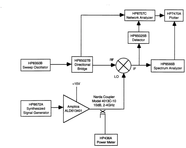
The test measurement setup for characterizing the MMIC double-balanced mixer is shown in Figure 3.1. A sweep oscillator was used for swept-frequency measurement over the 575-MHz RF input band. A directional bridge and detector are used to measure the mixer's conversion loss characteristics. A signal generator with amplifiers was used to produce the necessary LO drive levels. The test measurement setup modeled precisely the environment in which the mixer is intended to be used, e.g. no isolators are used at the RF, LO, and IF ports.
+15V
Narda Coupler Model 40130-10
10OdB, 2-4GHz
Figure 3.1 Test Measurement Setup for Mixer Characterization
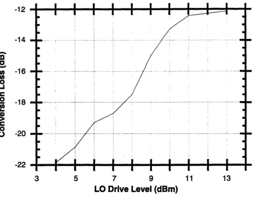
3.3 Local Oscillator Power Analysis
The LO drive level must be selected to achieve best conversion loss insensitivity. Mixer conversion loss was plotted over a range of LO power levels. The results are summa-rized in Figure 3.2.
-12 -14 -18 --20 -I I I I I ~I __I I I I 1 I 5 I I I l I 7 9 LO Drive Level (dBm) I I 13
Figure 3.2 Mixer Conversion Loss vs. LO Power
Conversion loss is insensitive at the LO drive level of approximately +13dBm, shown by the flattening of the slope in Figure 3.2. Reasonable LO power variation about this nominal point does not cause significant changes in mixer output level. The LO will therefore be designed to operate with an output level of +13dBm.
3.4 IF Filtering Analysis
IF filtering selects the IF band from the output at the mixer IF port. The spurious sig-nals outside of the band must be attenuated per receiver's spurious specifications. The
spuri-... --- ... --- .. - --- -- --- -- --- ---·-·--- ·----·-··---·--- ---I . U - . 1 ... ... ...-... ... ... ... -III -
-I-
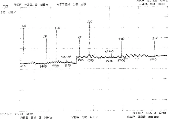
LJ Ious output of the mixer is shown in Figure 3.3. This measurement corresponds to the nominal LO drive level of +13dBm. ,MKR 2. 22 GH-SREF -20. 0 dBm ATTEN 10 dB -40. 60 dBm 12 d9/ 3L0 -!fL LO I
.. ...-
i ·
..
.. ....
6 -
. .i
.
.
-
.
.
.
... ....
CC425 7icS -= 2415 4 45 5.25 START 2.0 GHz STOP 12.0 GHz RES BW 3 MHz VBW 30 kH: SWP 300 meecFigure 3.3 Mixer Spurious Output
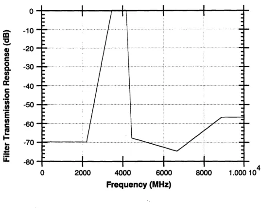
The IF filtering requirements are determined based on the spurious outputs. Filter rejection is the amount of spurious attenuation which must occur for the spurious to be -60dBc. A
Microsoft Excel worksheet was constructed to perform the calculations. The filter
-10 0 -20 o. -30 -40 0 "c -50 C -60
I-Ln -70 S -80 0 2000 4000 6000 8000 1.000 10 Frequency (MHz)
Figure 3.4 IF Filtering Requirements
The IF spurious analysis also determines the maximum bandwidth the receiver is capable of handling without violating spurious requirements. The bandwidth is constrained by the spuri-ous levels inband. Based on the spurispuri-ous analysis, it was determined that bandwidth up to 575MHz is achievable, ranging from 3.625GHz to 4.2GHz. With any significantly greater bandwidth, the conversion product 4LO-RF will fall inband, violating the receiver's inband spurious specification.
3.5
Alternate Mixer Implementations
Mixer performance presents a weak point in the system design. Poor isolation charac-teristics of the current mixer implementation makes IF filtering difficult. Its conversion loss characteristics require the use of a high-power local oscillator and high-gain devices through-out the receiver chain, thus increasing the system's power consumption as well as the chance for signal crosstalk.
Poor mixer performance may be explained by several factors. It is an experimental design utilizing a double-balanced topology. Isolation performance is critically dependent on the manufacturing tolerance of the input and output transformers. In addition, the lack of matching networks at the mixer's ports increases the amount of power with which the mixer must be driven in order to achieve acceptable performance. Current biasing is not utilized, in order to conserve power as well as to simplify the design. In the future, a current-biased de-sign may be considered to optimize conversion loss.
An alternative mixer source is being investigated. The mixer under consideration has a triple-balanced topology. Its conversion loss performance and drive level requirements are superior to those of the current mixer implementation. The implications of a better mixer are multiple: the LO power level may be reduced, IF filtering may be much simpler, and a larger receiver bandwidth than 575MHz may be realizable.
Chapter 4
Design of Local Oscillator
4.1 Introduction
The C-band local oscillator provides the 2225MHz signal required by the receiver to translate the 6-GHz RF band to the 4-GHz IF band [18]. This chapter addresses the design is-sues associated with the local oscillator realization.
4.2 Local Oscillator Performance Criteria
A summary of the major performance specifications of the local oscillator is given in
Parameter Requirement Units
Frequency (fo) 2.225 GHz nom
Output power +13 dBm nom
Output power stability ±1 dBm max
Short term stability
5Hz to 100Hz 0.5 Hz rms max
100Hz to 12kHz 25 Hz rms max
Long term stability
Temperature (-10/+550C) ±1 ppm max
Per month ±0.2 ppm max
Over life ±2 ppm max
Phase noise spectral density Offset from carrier:
10Hz -50 dBc/Hz max
100Hz -79 dBc/Hz max
1kHz -98 dBc/Hz max
2kHz -101 dBc/Hz max
100kHz -111 dBc/Hz max
1MHz and above -111 dBc/Hz max
Spurious output
Within f0±575MHz -73 dBc max
Harmonics of fo -40 dBc max
Output return loss 16 dB min
Table 4.1 Receiver Performance Requirements [19]
In addition to the specifications listed in Table 4.1, the LO must be designed to realize sav-ings in DC power consumption, size, and mass.
Among the performance parameters listed in Table 4.1, short and long term stability are key design parameters. Short term stability refers to frequency noise and fluctuations within random periods shorter than a few seconds. Long term stability describes slow changes of frequency due to factors such as aging. These two stability measures are illus-trated in Figure 4.1.
Frequency Noise Fluctuations 1 sec Short Term Stability I 1 min Aging I 1 hour Long Term Stability Sample Time
Figure 4.1 Frequency Stability [20]
Phase noise spectral density is another important performance specification. It may be defined as the ratio of the single sideband power of noise (Pssb) in a 1-Hz bandwidth fm Hz away from the carrier frequency to the total signal power (Ps) (Figure 4.2).
10
09
I . isI C)LU0 0 a M CL -- P 1Hz foFigure 4.2 Phase Noise Definition [20]
The LO's spurious output specifications are chosen in compliance with the overall re-ceiver spurious requirements. Spurious signals within f0o575MHz of the LO output will
ap-pear at the IF output of the mixer in the inband frequencies (3.625GHz-4.2GHz). Therefore, any spurious in the f0o575MHz band must be rejected to below -73dBc,* so that the
down-conversion unit may meet its inband spurious specification of -70dBc with some margin. LO's harmonic rejection requirement of -40dBc, in conjunction with proper IF filtering, will enable the receiver front end to meet its out-of-band spurious specifications.
The output return loss specification ensures proper impedance match at the LO-mixer interface.
4.3 Design Alternatives
The LO frequency is generated from a reference oscillator with excellent short- and long-term stability. Several approaches exist for using a reference signal to generate a stable RF signal. Different methods yield different phase noise performance [20] and result in trade-offs between DC power consumption, design complexity, reliability, mass, and size. These methods are described in detail in the following sub-sections.
4.3.1 VCO-based Phase-Locked Loop
The phase-locked loop (PLL) approach uses a voltage-controlled oscillator (VCO) to generate the 2225MHz LO signal. The VCO is locked to a low-frequency stable crystal oscil-lator. Figure 4.3 illustrates the block diagram of a VCO-based single-loop PLL design.
* The receiver's inband spurious specification must be applied to both (f0, f0+700MHz) and (f0-700MHz, f0)
bands, so that RF input ranging anywhere from 5.725GHz to 6.425GHz may have a spurious-free IF output ranging from 3.5GHz to 4.2GHz.
loop filter
frequency divider
Figure 4.3 VCO-Based Phase-Locked Loop Approach
General Operation
The 2225MHz output signal is generated by the VCO. Output of the VCO corre-sponds to its nominal oscillation frequency modified by the tuning voltage, as described by the equation
O2(t) = Co + Kou,(t)
* 02 = angular frequency of the VCO output
* coo = center angular frequency of VCO output
* Ko = VCO gain in s-IV- 1
* uy(t) = output signal of the phase detector loop filter.
The VCO output signal is coupled to a divide-by-n pre-scalar, which translates the frequency
of the signal
(0oo)
to match that of the reference signal (0 . The phase detector compares
the phase of the VCO signal with the phase of the reference signal. Based on the comparison, it generates an output error signal which is approximately proportional (within a limited range) to the amount of phase error,
d (t)= KdOe
* ud(t) = output of phase detector
* Kd = gain of phase detector in s-1V-1
* = phase error between VCO output and reference oscillator (XO) signals.
ud(t) consists of an average DC component and a superimposed AC component. The AC
component is undesirable for tuning the VCO frequency. It is rejected by the loop filter.
When the VCO deviates from its center frequency, a non-zero phase error 0e is gener-ated in the phase detector, which results in a non-zero output signal ud. After some delay, the loop filter would also produce a finite signal uf. This signal serves as the VCO tuning voltage and causes the VCO to change its operating frequency in such a way that the phase error fi-nally vanishes. This feedback mechanism synchronizes the VCO output with the crystal os-cillator reference signal in frequency as well as in. phase [26]. The net result is a LO output
signal at the frequency of the VCO but with the stability of the reference crystal.
Loop Filter Design
The loop filter removes the high-frequency components of the tuning signal to the
VCO. Loop filtering requirements are typically met by a first-order, low-pass active or
pas-sive RC filter [26]. An active design not only enhances the performance of the loop but also allows the inclusion of a sweep generator in the operational amplifier to perform frequency search during start-up [51]. Because the loop filter affects the phase and gain of the PLL, de-sign of the loop filter must take into consideration the best system phase and gain perfor-mance. Loop analysis entails examining the phase and gain of PLL components, then em-ploying a Bode plot or similar tools to calculate the phase and gain characteristics of the phase-locked loop's open transfer function. However, control loop analysis does not account
for the many second-order effects in PLL operation. Phase and gain effects are difficult to predict for most devices. Therefore, analytical design of the loop filter is often accompanied by empirical design, where a PLL breadboard is constructed and the optimal loop filter pa-rameters are determined empirically.
Phase Noise Calculation
Phase noise of a VCO-based PLL depends primarily on four factors: divide ratio of the loop and phase noise of the reference oscillator, phase noise of the VCO, and phase noise of the phase detector. Phase noise calculations are shown in Figure 4.4.
-40
i
-60-0
---80 -100 ... -120 - ---140 -i---160 1 --- --100 104
Frequency Offset from 2225MHz (Hz) Figure 4.4 VCO-based PLL Phase Noise
Table 4.2 lists the components specifications assumed in the above phase noise calculation. A temperature compensated crystal oscillator (TCXO) is used as the baseline reference signal source. A 139.0625MHz reference frequency is assumed, with a corresponding loop divide
ratio of sixteen = 32225MHz
139.0625MHz
- - TCXO-s-
TCXO (degraded) ---- phase detector - - - PD (degraded) t--- VCO ---t PLL ------ - ---WM:-6
10
' I" . . . . ." ' . ' " i . . .. . . ' I I ] J --- .... .... ---- ---- ---.... .. --- --- --- - ... --- --- --- ---- -- --- -- --- -7 : --- --- ---... ... .... - - --- -- -- .---- - --- -- --- -- --- -- --- --- -- --- -- --- -- --- -------- --- - ----
-
-
--- -- ------ ------ --- --- --- --- --- ---- --- 7: --- --- --- --- -- --- --- ---- --- --- -------Phase Noise PLL Component (dBc/Hz) TCXO [27] @ 10Hz -75 @ 100Hz -118 @ 1kHz -137 @ 100kHz -150 @ 1MHz -150
Phase detector noise floor [34] -150
VCO [35]
@ 100kHz -111
@ 1MHz -131
Table 4.2 VCO-Based PLL Components Phase Noise Specifications
Phase noise degradation by the loop is calculated as follows:
20 x log L = 20 x log(16) = 24.08dB
where L0 is the divide ratio of the loop. Inside the loop bandwidth, the PLL phase noise fi
equals the reference oscillator phase noise degraded by the loop noise, with a noise floor set by the phase noise of the phase detector (which is also degraded by the loop noise). Outside the loop bandwidth, the PLL phase noise equals that of the VCO. The loop bandwidth is se-lected so that overall PLL phase noise is minimized [20].
Second-Order PLL Design
The PLL approach is useful for generating high frequencies where a large reference pre-scaling ratio would be required. Utilization of higher order PLL topologies will result in a lower overall phase noise compared to that of the multiplier chain approach. Figure 4.5
loop filter phase
frequency divider
Figure 4.5 VCO-Based Phase-Locked Loop Approach (Second Order)
With the availability of low phase noise, high frequency reference oscillators, a synthesizer designer may reduce the pre-scaling ratio needed and thus attain acceptable phase noise with the single-loop PLL topology. In such cases, the additional complexity of the dual-loop ap-proach does not warrant the phase noise margin it provides. Moreover, multiple-loop designs require additional hardware in terms of VCOs, loop filters, phase detectors, dividers, and mixers, thus significantly increasing overall circuit area, complexity, and cost.
The stringent specifications for the 2225MHz LO implementation push the limits of the VCO-based PLL approach. In order to achieve optimal phase noise, the PLL must be de-signed with a wide loop bandwidth (20-50kHz). However, wide loop bandwidth compro-mises loop stability of the PLL. Therefore, the PLL design may not apply well to this fre-quency synthesis application.
4.3.2 DRO-Based Phase-Locked Loop
The dielectric resonator oscillator (DRO) phase-locked loop uses the high Q of dielec-tric resonator oscillator to obtain a low phase noise signal at 2225MHz. It is identical in de-sign to the VCO-based PLL except for the substitution of the VCO with the DRO, as shown in Figure 4.6. The result is much better phase noise outside the loop bandwidth. Consequently, the loop bandwidth may be smaller than that of a VCO-based PLL, making for an easier circuit design.
f=w0O dielectric
Dhase loop filter mannatnr
frequency divider
Figure 4.6 DRO-Based Phase-Locked Loop Approach
Phase Noise Calculation
Figure 4.7 illustrates the projected phase noise performance calculation for the DRO-based PLL. This figure shows that DRO-DRO-based PLL offers better phase noise performance
- - - TCXO -- TCXO (degraded) -40 ... ... ... ...
-...
--...
phase detector .-- - PD (degraded)i...ii
-60 . ..- t - DRO :----
---
---
---
---
-
...
---•,-- PDROii
-80
----
-o-
_0
: ...
:
: :
.
..
.
... ::
--:::
Z -120a.
-140 - --16 0 " " 1 100 10 10Frequency Offset from 2225MHz (Hz) Figure 4.7 DRO-BASED PLL Phase Noise
The methodology for calculating DRO-based PLL phase noise is identical to that for VCO-based PLL phase noise, except the lower DRO noise floor is used in place of the VCO noise floor (for outside of the loop bandwidth). Optimal loop bandwidth remains at 100kHz.
Summary
VCO DRO
Phase noise -97dBc/Hz @ 50kHz -100dBc/Hz @ 10kHz -105dBc/Hz @ 100kHz -125dBc/Hz @ 100kHz Bias supply 50mA @ +15VDC 100mA @ +15VDC Size 0.5" x 0.2" x 0.5" 2.9" x 2.0" x 0.9"
Weight 1.7g 894g
Table 4.3 Comparison between VCO and DRO [36]
Table 4.3 compares the two different implementations of the free-running oscillator. The DRO consumes twice as much power, occupies much larger volume, and has significant more weight as compared to the VCO. In addition, temperature stability of the dielectric ma-terial is a major risk factor. The marginal phase noise advantage of the DRO-based PLL ap-proach does not warrant such severe penalties. The DRO-based PLL design was not pursued in favor of other LO implementation approaches.
4.3.3 Multiplier Chain
The multiplier chain generates the 2225MHz output signal by multiplying up the fre-quency of a low-noise, high-stability crystal oscillator using multiplier stages. A block dia-gram is shown in Figure 4.8.
comb bandpass comb - bandpass
generator filter generator filter driver bandpass amplifier xilter
f=wO/(nlxn2) multiplier stage #1 multiplier stage #2 f=wO
(x nl) (x n2)
General Operation
The multiplier chain employs a series of multiplier stages to generate the desired LO output frequency from the much lower reference oscillator (XO) frequency. Each multiplier stage consists of a comb generator and a bandpass filter. The comb generator generates monics of its input signals at its output. The bandpass filter then selects the appropriate har-monic to realize the desired frequency multiple. Comb generation may be implemented with a variety of devices, including step-recovery diodes and amplifiers operated in the non-linear region.
The multiplier chain approach is the least desirable for frequency generation when a large multiplication factor is required. Several multiplier stages would be needed in such cases. Each additional multiplier stage adds to the overall insertion loss and DC power con-sumption. However, with the recent availability of low-noise, high-frequency crystal oscilla-tors, the number of multiplier stages can be significantly reduced.
Phase Noise Calculation
Phase noise of the multiplier chain is the phase noise of the reference oscillator de-graded by the frequency multiplication factor [20]. The phase noise calculations are shown in Figure 4.9. In the multiplier chain, the crystal oscillator presents the only significant contri-bution to overall phase noise. Unlike the phase-locked approaches, no other noise compo-nents in the multiplier chain contribute in a significant way. The amplifiers' low noise figures should be lower than the most stringent phase noise requirement of the LO signal
(-150dBc/Hz at >1MHz offset) [20].
TCXO is used as the baseline reference signal source. A 139.0625MHz reference fre-quency is assumed, with a corresponding multiply ratio of sixteen. The TCXO phase noise specifications are the same as those used for the VCO-based PLL and DRO-based PLL phase
noise calculations (refer to Table 4.2). A phase noise margin of 5dBc/Hz is added to phase noise degradation, to account for secondary phase noise contributions by components other than the TCXO.
-40 -60 -80 0 m a. -100 S-120 * -140 -160
100
10
4Frequency Offset from 2225MHz (Hz)
106
Figure 4.9 Multiplier Chain Phase Noise
The amount of phase noise degradation is as follows:
20 x log-• = 20 x log(16) = 24.08dB
where Lo is the total multiply ratio. The amount of phase noise degradation due to the
mul-fl
tiplication process may be attenuated by several means. Negative feedback at low frequency may be designed into the amplifiers. Some negative feedback has also been introduced at RF frequency in the past to stabilize the transconductance [20].
53 S...m ultiplier chain .... -..--- .... . ... ... ... - --- ... .
...
---
-
-
--
-
---
-
-
---
--. "•. ... ... ; ... I ... ... ... ... ... 4 ... ... . --- ---. .. .. . ...---·--- --- ...- --4- --- ---... --- ... ... --- ... -- ..."
n
< >
-
.---.---" .---.---"... ... ... ; ... III I I I l ll Il HI I I 11 1 l l Il 1 1H tl t l I ( II ll I I I Il III I I_ =4.3.4 Selection of Approach
The topology to be used to implement the C-band receiver LO was chosen based on phase noise characteristics, spurious performance, DC power consumption, size, reliability,
and engineering risk. The following considerations were used:
Phase Noise
All three approaches are capable of meeting phase noise specifications of the LO. In general, the multiplier chain approach has the worst phase noise, followed by VCO-based PLL, and DRO-based PLL. PLL designs typically have better phase noise characteristics than the multiplier chain because of the availability of a multiple-loop configuration for high fre-quency synthesis. In higher-order PLL topologies, multiple phase detectors and adjustment capabilities allow the overall phase noise to be less than that of a simple degradation of the crystal oscillator phase noise by the pre-scaling ratio, as in the case of the multiplier chain. However, in this C-band receiver LO application, availability of a low-noise, high-frequency
crystal oscillator [27] and small multiplication factor obviate the need for multiple loops. As illustrated in Figure 4.10, single-loop versions of the VCO-based PLL and DRO-based PLL present only marginal phase noise advantage over the multiplier chain. In addition, the phase noise performance of the multiplier chain approach is less sensitive to power supply noise.
-40
--60 -N -80 - S-100-Z -120-to L -140- -160--... -- Specification S.••• multiplier chain ... .. ... --- - - P LL-.. L-..L-..L-..L-..L-..L-..L-...
.
---
...- !-
-
P
D
R
O
-
-
--
...
--
-
-
...
...
---N...
1
.... ...
.
--
----
... ...
--
----
----
---
---
-
---
-
--
-
---
--
--
0
---
---
...
---
-
-
---
-
----
-
...
-
----
----
----
---
i-
-
-
-
----
-
---
- -
....
...
----
----
-
--
---
I
... ...---·--- ·--- --- 4 ·- ·- ---- - - -·--- -- ---- --- --- --- ---... -... ... - ... I I t 1 J 1 100 104 106Frequency Offset from 2225MHz (Hz)
Figure 4.10 Phase Noise Comparisons
Spurious Performance
The PLL designs will have greater difficulty meeting the spurious specifications of the LO compared to the multiplier chain approach. In the PLL, inband spurious due to power supply noise are difficult to remove. In the multiplier chain, out-of-band harmonics are gen-erated but may be removed using filters.
DC Power Consumption
When compared to the PLL approaches, the multiplier chain approach has consumed greater DC power in the past. However, with the availability of low-power comb generators
![Figure 1.1 Block Diagram of Communications Transponder [17]](https://thumb-eu.123doks.com/thumbv2/123doknet/14676848.558194/21.918.234.662.116.407/figure-block-diagram-communications-transponder.webp)
![Figure 4.1 Frequency Stability [20]](https://thumb-eu.123doks.com/thumbv2/123doknet/14676848.558194/41.918.236.668.109.447/figure-frequency-stability.webp)