Analysis of Materials Properties of Thin Film
Structures for Thermoelectric and
Thermophotovoltaic Applications
by
Brian K
.
Baum
Submitted to the Department of Materials Science and Engineering
in partial fulfillment of the requirements for the degree of
Bachelor of Science in Materials Science and Engineering
at the
MASSACHUSETTS INSTITUTE OF TECHNOLOGY
June 2010
@
Massachusetts Institute of Technology 2010. All rights reserved.
Signature redacted
Author ...
Department of Materials Science and Engineering
May 13, 2010
/ 17
Certified by
...
Signature
redacted
Eugene A. Fitzgerald
Professor of Materials Science and Engineering
Thesis Supervisor
Signature redacted
A ccepted by ..
...
Lionel C. Kimerling
MASSACHUSETTS INSTITUTE
Chairman, Undergraduate Committee
OF TECHNOL GY
JUL 1
0 2017
MITLibraries
77 Massachusetts Avenue
Cambridge, MA 02139 http://Iibraries.mit.edu/ask
DISCLAIMER NOTICE
Due to the condition of the original material, there are unavoidable flaws in this reproduction. We have made every effort possible to provide you with the best copy available.
Thank you.
The images contained in this document are of the best quality available.
Analysis of Materials Properties of Thin Film Structures for
Thermoelectric and Thermophotovoltaic Applications
by
Brian K . Baum
Submitted to the Department of Materials Science and Engineering on May 13, 2010, in partial fulfillment of the
requirements for the degree of
Bachelor of Science in Materials Science and Engineering
Abstract
Metal-organic chemical vapor deposition (MOCVD) was used to grow InAsP graded layers and AlAs/GaAs superlattices for materials studies related to thermophoto-voltaics and thermoelectrics respectively. High resolution x-ray diffraction (HRXRD) was used to determine the As concentration in each of the InAsP layers. Arsenic concentration was found to vary linearly with the percentage of AsH3 in the
reac-tive gas flow up to 60 % deposited, and had an asymptotic relationship for higher incorporated concentrations. Higher growth temperatures reduced As incorporation. Transmission electron microscopy (TEM) images were used to determine layer thick-nesses. The growth rate of InAsP layers was found to be independent of growth temperature and the percentage of As. Superlattice samples with 0 %, 5 %, 10 %, and 20 % variations in the superlattice period were grown via MOCVD and analyzed using HRXRD. The intensities of the satellite peaks were found to decrease and broaden with increasing variation in the period length and disappeared completely in samples with up to 10 % variation. Thermal conductivity measurements performed using an optical pump-probe technique showed lower thermal conductivities for samples with greater variation. The irregularity of the superlattice period is believed to enhance the structure's ability to impede phonon propagation.
Thesis Supervisor: Eugene A. Fitzgerald
Acknowledgments
I would like to offer my greatest thanks to Adam Jandl and Mayank Bulsara for their
guidance and assistance throughout the entirety of my thesis project, for producing samples, and for performing collaborative analysis on those samples. I would also like to thank Scott Speakman, whose training, maintenance of the x-ray lab, and advice on everything x-ray related made data collection possible. I also thank Maria Luckyanova, who is responsible for all thermal conductivity data provided. Finally,
I owe my respect to my advisor, Professor Eugene Fitzgerald, who has provided me
with a stellar research group to work with, an interesting project, and a target for my admiration.
Contents
Introduction . . . . Thermophotovoltaics... Thermoelectrics . . . . Literature Survey . . . . Thermophotovoltaics . . . . . Thermoelectrics . . . .Methods & Experimental Procedure
Thermophotovoltaics . . . . . Thermoelectrics . . . . R esults . . . . Thermophotovoltaics . . . . . Thermoelectrics . . . . D iscussion . . . . Thermophotovoltaics . . . . . Thermoelectrics . . . .
Summary and Conclusions . . . . .
Thermophotovoltaics . . . . .
Thermoelectrics . . . .
Suggestions for Further Work . . .
Thermophotovoltaics . . . . . Thermoelectrics . . . . 1 3 . . . . 1 3 . . . . 1 5 . . . . 1 7 . . . . 1 7 . . . . 1 9 . . . . 2 1 . . . . 2 1 . . . . 2 3 . . . . 2 4 . . . . 2 4 . . . . 3 3 . . . . 3 8 . . . . 3 8 . . . .I . . . . . 4 0 . . . . 4 1 . . . . 4 1 . . . . 4 2 . . . . 4 2 . . . . 4 2 Appendix . . . . ... . . . . 42 43
List of Figures
1 As incorporation as a function of temperature and AsH3 flow fraction
taken from Venkataraghavan, et al. [19]. . . . . 18
2 Thermal conductivity as a function of superlattice period and temper-ature taken from Capinski, et al. [6]. . . . . 20
3 (004) diffraction of first three calibration samples: a) three InAsP lay-ers grown at 650 C with a N2 carrier gas, b) three InAsP layers grown at 650 C with a H2 carrier gas, and c) five InAsP layers grown at
575 C with a N2 carrier gas. . . . . 24
4 (004) diffraction of six layer samples grown with a N2 carrier gas at a) 575 C and b) 650'C. . . . . 26 5 Percentages of As incorporated into the layers as a function of
temper-ature and the ratio of AsH3 in the gas flow. . . . . 28 6 (224) diffraction of 6 layer InAsP graded layers grown at a & c) 575 C
and b & d) 650'C. . . . . 29 7 w versus relative w scan of the six layer InAsP sample grown at 650 C. 30
8 TEM of the six layer InAsP sample grown at 575 C. The interfaces between layers are visible as clusters of dislocations. . . . . 31 9 (004) diffraction of AlAs/GaAs superlattice structures with a) 20 %
variation, b) 10 % variation, c) 5 % variation, and d) 0 % variation. . . 33 10 A Leptos model of a (004) x-ray diffraction of a perfect AlAs/GaAs
superlattice is overlayed on the HRXRD results from the 0 % variation superlattice. . . . . 35
11 TEM images of the a) 0 % variation, b) 5 % variation, c) 10 % variation, and d) 20 % variation superlattices. . . . . 36
12 Thermal conductivity measurements at pump modulation frequencies of a) 3.62 MHz, b) 5.83 MHz, c) 9.1 Mhz, and d)11.5 Mhz for superlat-tices with 0 %, 5 %, 10 %, and 20 % variation in period length. .... 38 13 AsH3 flow rate, growth temperature, and flow gas of each sample layer
List of Tables
1 (004) diffraction results with calculated As concentrations for early
MOCVD calibration samples . . . . 25
2 (004) diffraction results with calculated As concentrations for the six layer sam ples . . . . 27
3 (224) glancing angle results for six layer InAsP graded layers . . . . . 30
4 Layer thicknesses from TEM . . . . 32
5 Superlattice w peak positions . . . . 34
6 Superlattice period from satellite peaks . . . . 35
Introduction
The United States Energy Information Administration reported in 2007 that the world's electrical consumption was over 17,000 billion kilowatt hours with the United States responsible for 3,000 billion kilowatt hours [1]. Demand will only continue to grow as the standard of living increases worldwide, but the supply of fossil energy the modern world is so greatly dependent on is finite. Thus, one of the greatest challenges for the scientific and engineering communities is underway as new devices and systems are being designed to reduce the need for fossil energy, be it through the utilization of energy sources previously untapped or though increases in efficiency.
Thermophotovoltaics and thermoelectrics are two technologies that can help re-duce the need for fossil energy by providing alternative ways of power generation. Both technologies are currently limited in application due to low efficiencies, but a considerable research initiative is underway to make them commercially viable
[15, 13]. At the forefront of this effort is the drive for a better understanding and
con-trol of material properties via materials science. Solid state technologies are extremely demanding from a materials engineering standpoint, as a multitude of different prop-erties must be optimized before the device can become a reality. The efficiency of thermoelectrics, for example, are generally measured by ZT, a collection of mate-rials properties, which will be explained later. The advent of nanotechnology and the realization of the size dependence of various properties have greatly enhanced the toolset of the materials engineer, and have enabled greater optimization of these devices than previously possible [4]. This thesis focuses on the analysis and charac-terization of early attempts at designing graded layers of InAsP on InP to provide a virtual substrate for a thermophotovoltaic device and superlattices of AlAs/GaAs for thermoelectrics.
Thermophotovoltaics
Thermophotovoltaic (TPV) cells are semiconductor diodes that absorb light within the infrared spectrum. The thermal energy of the infrared source is transferred into
electrical energy by a TPV system. Given the wide availability of heating methods, TPV systems could be coupled to a number of thermal sources including combustion reactions, the sun, or furnaces in industrial processes such as glass manufacturing [151.
To use a solar source, a TPV system must have an emitter material that is heated by the sun to become a grey body. The sun's black body radiation at 5800 C has high energy but a relatively low intensity of less than 1 W/cm2 [3]. Through the use of solar
concentrators, the emitter material can reach temperatures up to 1500 C, and the close proximity of the emitter to to the TPV cell can create intensities greater than 10 W/cm2 [3]. Theoretical predictions indicate that for intensities of 0.001 W/cm2 to
5000 W/cm2, solar TPV systems can have efficiencies roughly two times greater than
photovoltaics [18].
The spectrum of light from the grey body will not be as broad as the light emitted from the sun due to the loss of the higher energy radiation. The spectrum can further be restricted by using a selective emitter or by using reflectors and filters [15]. When absorbed in the TPV cell, any radiation with greater energy than the band gap will only contribute the band gap energy to electrical generation; the rest is wasted as thermal energy. Radiation with energy less than the band gap will not be absorbed by the TPV cell at all. Both of these sources of inefficiency can be reduced by tailoring the spectrum of emitted radiation, increasing the overall efficiency of the TPV cell. For grey body emitters, the TPV cell should possess a band gap of approximately
0.5-0.6 eV [7]. Alloys such as InAsP, GaAsSb, and InGaAs all have band gaps in this region and it would be preferable to deposite these films on an InP substrate. The lattice constant of InP is smaller than that of the III-V ternary alloys, so a graded layer is used to bridge the difference in the lattice size. This graded buffer layer enables a virtual substrate by incrementally shifting the lattice size from that of InP to InAsP by incorporating more As in each step.
In this thesis, the author examines a number of graded InAsP layers grown on an InP substrate via metal-organic chemical vapor deposition (MOCVD). Layers are analyzed using high resolution x-ray diffraction (HRXRD) to determine relative As incorporation to calibrate the MOCVD system for future growths. Various growth
conditions are tested, including chemical flow rates, growth temperature, and the inert carrier gas. The incorporation of As is found to be linear at low levels of incorporation but eventually reaches a saturation point, similar to previously published work [19]. The saturation limit is much higher than reported elsewhere, and may be due to differences in the MOCVD growth system or in the level of strain present in the InAsP layers. Transmission electron microscopy (TEM) images were used to measure layer thickness and observe dislocation aggregation at interfaces.
Thermoelectrics
Thermoelectrics are solid state devices that convert a temperature differential to an electric potential (Seebeck effect) or an electrical potential to a temperature differ-ential (Peltier effect) [8]. To generate power, a temperature differdiffer-ential is created across n- and p-type doped materials positioned parallel to one another. The greater mobility of the majority carriers on the hot side of the material imparted with the additional energy from the higher temperature creates a net flux of carriers down the temperature gradient, producing a current and an electrical potential across the device [2]. Thus, a thermoelectric device is capable of harvesting heat energy and directly transforming it into useful electrical energy-a system that would be ideal for recovering efficiency losses due to waste heat from countless industrial and energy intensive processes.
The reverse case is also possible, in which an externally provided flow of carriers can be used to remove heat from one surface of the device [11]. Solid state tem-perature control offers the benefits of no moving parts, no working fluids, and small scale. These devices also have rapid response times and are robust enough to sur-vive and perform well in demanding environments. A number of niche markets have evolved around these selling points, such as cooling for laser diodes, where heat is generated but can be detrimental to device performance or lifetime [2]. Currently, the efficiencies of thermoelectrics prevent them from reaching wider use in electri-cal energy generation or solid state temperature control. In terms of temperature control, efficiency is often quoted as a percentage of Carnot efficiency, which is the
thermodynamic maximum efficiency [11]. Present thermoelectric devices are just over
10 % efficient, whereas compressor-based units used in kitchen refrigerators operate
at approximately 30 %, and commercial sized air conditioners operate near 90 % [11]. The challenge of increasing the efficiency of thermoelectrics is best summarized in the thermoelectric figure of merit, ZT,
c-S2
ZT = T (1)
where o- is the electrical conductivity, S is the Seebeck coefficient, r, is the thermal conductivity, and T is the temperature multiplied to both sides to make the figure of merit dimensionless [12]. The difficulty in engineering high ZT materials is that all the terms are usually interrelated, so that any gain in one is usually lost in another
[13]. For example, metals possess high electrical conductivity, but also have high
thermal conductivity. The reverse case of low thermal and electrical conductivity is seen in glasses, such as SiO2. Accordingly, the best thermoelectric materials would
be described as "phonon-glass electron-crystal," where phonons will have poor con-ductivity like in a glass, and electrons will have high concon-ductivity like in a crystal
[81.
So far, the most efficient thermoelectrics have been doped or alloyed semiconductor materials [201.
A more recent tactic to increase ZT has been to incorporate nanoscale
struc-tural engineering, specifically the use of thin film superlattices, into thermoelectric designs
[5].
The incorporation of a second level of periodicity of a different material in superlattices may allow for individual manipulation of electron or phonon trans-mission properties. The work of this thesis focuses on a new study of superlattices in which the period of the superlattice varies by a certain percentage through the entire sample. The effect of the change in periodicity is analyzed using HRXRD, in which the disappearance of satellite peaks is noticed for samples with high percentages of variation. Layer thicknesses are observed using TEM, and preliminary thermal con-ductivity measurements indicate the loss of regular periodicity may suppress thermal conductivity.Literature Survey
Thermophotovoltaics
InAsP thermophotovoltaic devices have been grown on InP substrates using InAsP graded layers via molecular beam epitaxy
[3].
The virtual substrate consists of three layers of n-type InAsP with increasing As concentration targeted as 16 % As, 28 %As, and 34 % As [3]. The relaxation of the graded layer was assessed using HRXRD of the symmetric (004) direction, asymmetric (115) direction, and a reciprocal space map [3]. From these tests, the graded layer was found to have a relaxation of 97% and a residual strain of 0.8 % [3]. The InAsP TPV structure was tested and possessed a quantum efficiency greater than 90 % for a bandgap of approximately 0.60 eV [3]. Although the growth method was different, this paper demonstrated the growth of an InAsP TPV diode on an InAsP virtual substrate, which is one of the eventual goals of this project. The use of HRXRD to extract the concentration of As within the graded layer was also used in this thesis.
Gas Flux Dependence
Chemical vapor deposition has also been used to create InAsP layers, where the target As and P concentrations within the layers are selected through a combination of deposition temperatures and a ratio of AsH3 to PH3 gas flow [19]. Studies in the
creation of InAsP quantum wells revealed that the partial pressure of AsH3 in the flow
gas has been found to be approximately 100 times lower than the percentage of As in the deposited layer at deposition temperatures of 550 C [19]. The As concentration also reached a saturation point in this study of quantum well structures that can be seen in figure 1, at which point increasing partial pressure of AsH3 produced a
diminishing increase in incorporated As [19]. Strain caused by the lattice mismatch and the larger atomic radii of As compared to P may have been the source of the saturation in the quantum well structure, as tests with unstrained, fully relaxed, systems were capable of incorporating much higher percentages of As [19].
r k
r
a
550
gCa
relaxed
0.7. 04 1 r b2Ca) 550 C a 0t 4-(b) 600
00
0WOW 0.2 ()65O 0.1 0.0 0.000 0.002 0.04 0.008 0,008 0.010 0.012 0.014AsI
3f(AsH
3+PH
3)
Figure 1: As incorporation as a function of temperature and AsH3 flow fraction taken
from Venkataraghavan, et al. [19].
Temperature Dependence
Arsenic incorporation is temperature dependent, and increases with decreasing tem-perature between 625 0C and 550'0C as can be seen in figure 1 [19]. This trend is
explained by energetic differences between AsH3 and PH3, primarily the efficiency of
pyrolysis and volatility [19]. The kinetics of pyrolysis are a function of temperature, and the decomposition of PH3 varies greatly within the typical deposition
temper-atures of CVD-ranging from 85
%
at 900'0C to 25%
at 600'0C [19]. Arsenic, on the other hand, maintains 100 % decomposition at temperatures as low as 580'0C [19]. The balance between uptake and desorption of As and P is also temperatureThermoelectrics
Accurate measurements of ZT are difficult to obtain for thin film systems, as the extremely small length scales and the necessity of a substrate make temperature measurements through the material challenging. Additionally, no system has the ability to simultaniously test all of the parameters within ZT, so a variety of tests must be conducted, often requiring their own individual samples. These challenges can and have led to disagreements within the community on the actual values of ZT and its constituent parameters, particularly thermal conductivity.
AlAs/GaAs superlattices have been studied extensively, since the similarity in lattice size allows for quality epitaxial growth with minimal defects [9, 21, 6]. With minimal defects, the effects of the superlattice can be tested independently and with confidence. Theoretically, superlattices with small enough periods should have ther-mal conductivities approaching those of the AlO.5GaO.5As bulk alloy, and the earliest
studies of this system revealed that superlattices with periods as small as 5 nm were still more thermally conductive than the bulk alloy when tested using an ac calori-metric method [21]. These findings were later refuted by another study in which at room temperature, superlattices with layers under 25nm thick were found to have thermal conductivities less than the AlO.5GaO.5As bulk alloy with a continued trend of
decreased conductivity down to 1 nm when using an optical pump and probe method
[6]. Thermal conductivity was also found to decrease with increase temperature from 100 K up to 400 K [6]. The superlattice period and temperature dependence of
ther-mal conductivity can be seen in figure 2. Great importance, therefore, must be placed on the testing method and temperature to compare values successfully.
The decrease in thermal conductivity imparted by short period superlattice sys-tems still lacks an all-inclusive explanation, but can be explained as interference of phonon propagation due to the heterointerfaces possessing different atomic masses and atomic radii, on a length scale smaller than the mean free path of the phonon [6]. The superlattice may modify the phonon-dispersion relation, in a way that creates new gaps, particularly when the wave vector of the phonon normal to the superlattice
020
0.150.05
0.00
a a200
a300
TEMPERATE
(K)
Figure 2: Thermal conductivity taken from Capinski, et al. [6].
as a function of superlattice period and temperature
planes is an integer mulitple of ' where dSL is the period of the superlattice [6]. Another possibility is the promotion of Umklapp scattering, in which a phonon's total momentum changes by a reciprocal-lattice vector [6]. The energy required to cause Umklapp scattering is related to the reciprocal-lattice vector, and since the magni-tude of the shortest reciprocal-lattice vector is smaller in a superlattice structure, the energy barrier is reduced and more scattering occurs [6].
--
40x40 -o-6x6
-x-45225
-a-3x3
-o-
17x17-x-2x2
-e*
lo-x10-+1xI
A",100
400
A , ... . ... ...-Methods & Experimental Procedure
All samples were created in the Substrate Engineering Laboratory (SEL) at MIT by
Dr. Mayank Bulsara using a MOCVD system. Growth conditions are listed in the appendix. TEM analysis was performed by Adam Jandl, Dr. Mayank Bulsara and the author.
All HRXRD analysis was carried out on a Bruker D8 3-axis HRXRD system using
a copper source, a four bounce Ge (220) monochrometer on the source side, and a triple bounce Ge (220) monochrometer on the detector side. Symmetric (004) scans were performed on all samples and asymmetric (224) scans were conducted on two InAsP graded layers grown after the initial system calibration. An w -relative W map was extracted for one InAsP graded layer.
Thermophotovoltaics
GrowthThree InAsP graded layer samples were grown on an InP substrate in the MOCVD system under different growth temperatures and carrier gasses. HRXRD analysis of these samples was used to determine the percentage of As incorporated into each layer, and these results were matched to the growth conditions to determine what effects growth temperature, carrier gas, and AsH3 partial pressure had on As incorporation.
Two samples were grown at 650 C with N2 and H2 carrier gases. Each sample
contained three layers targeted to be InAsO.2PO.8, InAsO.4PO.6, and InAso.6PO.4. The
third sample was grown at 575 C with an N2 carrier gas and contained two additional
layers targeted to be InAso.0 5PO.95 and InAsO.1PO.9 for a total of five layers. Growth
times and flow rates were selected to create layers 500 nm thick.
Two additional InAsP graded layers were grown with shorter growth times and higher Trimethylindium (TMI) flow rates using a calibration curve created from the first three growths. These samples were composed of six layers targeted to be InAso.05PO.95, InAsO1 Po.9, InAso.15PO.85, InAsO.2PO.8, InAso.25PO75, and InAsO.3PO7
Analaysis
The As concentration in each layer was determined based on the perpendicular lattice constant extracted from Bragg's Law, with the assumption that the lattice constant is linearly related with As concentration. The perpendicular lattice constant of the
film, a1, is then
a =
[
s(OB) 1] x a. + a. (2) sfn(OB + AOsym)where 0
B is the substrate Bragg angle, A~Oym is the angular difference between
the substrate and film peak, and a, is the substrate lattice constant [10]. This equa-tion assumes the film is completely relaxed so that a1 = all and all of the relevant information is contained in a single (004) scan. Since each layer is several hundred nanometers thick, the majority of the x-ray signal will come from the bulk, which should remain unstrained due to the presence of dislocations at the interfaces between the layers. Extraction of the concentration of As in the layer can then be extracted
according to
composition = - a (3) af - a.
where af is the lattice constant of the film.
Asymmetric scans offer additional insight into the state of the film by collecting the lattice constant perpendicular to the substrate, a1, and parallel to the substrate,
all, according to
a - a. x -sin(OB,asym) X cos(0) (4)
sin(OB,asym + AO) Cos(0 + AO)
all = as x x(OBasym) sin(o) (5)
sin(OB,asym + AO) sin(O
+
AO) where 9B,asym is the Bragg angle for the asymmetric plane (224),
#
is the anglebetween the asymmetric and symmetric planes in the cubic lattice (arccos( '), AO
substrate peak [10]. By comparing these two lattice constants, it is possible to de-termine the amount of deformation and strain within the layer. Epitaxial growth of incommensurate crystal systems forces all of the layer to match the substrate, and the poisson effect will reduce or increase a_L accordingly.
Thermoelectrics
GrowthFour samples were created with different variations in the periodicity of the super-lattice composed of 8 nm AlAs and 8 nm of GaAs with 219 repeat units. One sample was a perfect superlattice with no variation, the others samples contained 5 %, 10 %,
and 20 % variation based on the 8 nm thickness.
Analysis
The periodicity of interfaces between the different material systems in the superlattice structure create an x-ray diffraction signature similar to the periodicity seen within a crystal. The location of these satellite peaks relative to the material peak can be used to find the thickness of the superlattice period, just as the lattice parameter of a crystal can be found using Bragg's Law. The superlattice satellite peak location is related to the period size according to
2sin(0mat ) - 2sin(Ost) n(6)
A A
where 0mat is the Bragg angle of the material, Ost is the diffraction peak of the satellite, A is the wavelength of the source, n is the order of the diffraction, and A is the supperlattice period [16].
Thermal conductivity measurements were performed by Maria Luckyanova using an optical pump-probe technique detailed elsewhere [17]. The superlattice samples were tested at 202 K and 296 K and at four different pump modulation frequencies:
3.62 MHz, 5.83 MHz, 9.1 MHz, and 11.5 MHz. An x-ray model of the perfect
Results
Thermophotovoltaics
Early MOCVD Calibration Samples
Figure 3 contains the (004) diffraction results collected from the first three calibration samples. All layer peaks are over 0.4 degrees offset from the substrate peak, which is considerable given InAs is approximately 1.1 degrees offset from InP. All layers, therefore, must have incorporated more As than intended.
104 10 3 10 2 10 1 1 0 . 30.6 30.8 31.0 31.2 31.4 31.6 31.8
I
30.6 30.8 31.0 31.2 31.4 31.6 31.8 30.8 31.0 31.2 31.4 a -20 (dfg) 31.6 31.8 32.0Figure 3: (004) diffraction of first three calibration samples: a) three InAsP layers grown at 650 C with a N2 carrier gas, b) three InAsP layers grown at 650 C with a
H2 carrier gas, and c) five InAsP layers grown at 575 C with a N2 carrier gas.
C) 10 4-10 2 10 2_ 30 1024 10 3 101 .6
Over incorporation of As was confirmed after analyzing the peak positions and extracting As % according to equation 2. These measurements are listed in table 1. The full-width half-maximum (FWHM) is listed within table 1 as well and can be used as an indicator of the accuracy of the measurement. All of the peaks were of relatively low intensity compared to the substrate and experienced some overlap for similar As percentages. The peak smearing caused by overlapping peaks made accurately determining the center difficult. For example, the fifth peak from the sample grown at
575 'C could not have contained 104.61 % As because that is impossible-the error was likely the result of difficulty determining the true peak position or due to incomplete relaxation of the InAsP film.
Table 1: (004) diffraction results with calculated As concentrations for early MOCVD calibration samples Sample Layers 650'C in N2 1 2 3 650'C in H2 1 2 3 575'C in N2 1 2 3 4 5 AO -0.6648 -0.9158 -1.0644 -0.6336 -0.8760 -1.0553 -0.4772 -0.8281 -0.9116 -1.0861 -1.1501 FWHM 0.0025 0.0360 0.0309 0.0027 0.0205 0.0150 0.0220 0.0679 0.0691 0.0520 0.0720 Measured As % 59.46 82.63 96.53 56.61 78.93 95.67 42.41 74.49 82.24 98.57 104.61
AsH3 Flow/Total Flow
0.0253 0.0750 0.2250 0.0253 0.0750 0.2250 0.0125 0.0175 0.0250 0.0750 0.2250
The partial flow rate of AsH3 is also provided in table 1 to compare the percentage
of As incorporated within a layer to the flow rate that produced it. The carrier gas has at most a very minimal effect on the incorporation of As, with the H2 carrier gas
producing concentrations approximately 1 % less than the N2 carrier gas at the same
Six Layer Growths
The six layer InAsP graded layers were grown with reduced AsH3 partial flow rates, and the effect on As incorporation is apparent in figure 4 by the reduction in the offset between most of the layers and the substrate peak. The increase in peak number and decrease in range of offset resulted in much higher peak density. This made it difficult to determine the individual peak positions to extract the As concentration in each layer. CD 0 ZCD C 105 10 -10 3 10 -10 10 -0 10 -104 _ 10 -102 104 -31.0 31.2 31.4 31.6 o-20 (deg) 31.8 32.0
Figure 4: (004) diffraction of six layer samples grown with a N2 carrier gas at a)
575'C and b) 650 C.
Table 2 contains the raw HRXRD results, measured percentage of As calculated with equation 2 within the deposited layers, and the AsH3 partial flow rate.
Measure-a)
ments of the As percentage for the layers between the substrate and the top layers are approximations, as finding peaks for these layers was difficult due to the smeared intensity. These layers do not have a quoted FWHM since the peak is barely dis-cernible from the elevated background and was not determined by the peak fitting software. Measured As percentages were much closer to the targeted values quoted in the methods section compared to the first three samples, although measured percent-ages still varied from the targeted amounts. The percent error of the sample grown at
575 'C ranged from 30 %-50 %, and As percentages were always higher than targeted. The percent error of the sample grown at 650 'C was smaller, only 1 %-30 %. Low concentrations were hardest to reach, as both samples had their greatest error for the
5 % target concentration.
Table 2: (004) diffraction results with
samples
calculated As concentrations for the six layer
Sample Layers AO FWHM Measured As %. AsH3 Flow/Total Flow
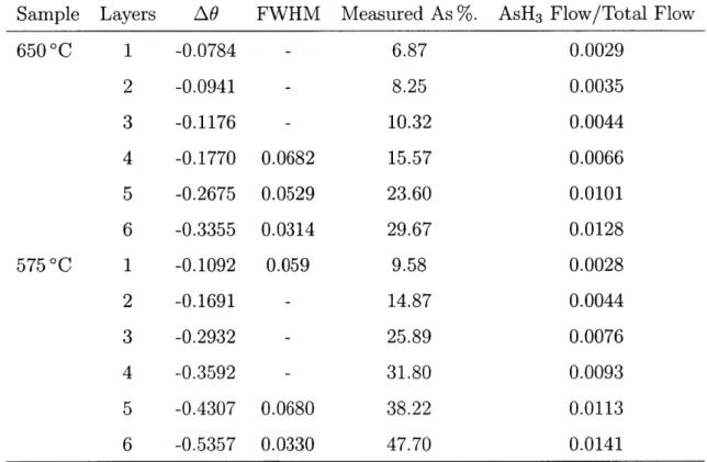
650 C 1 -0.0784 - 6.87 0.0029 2 -0.0941 - 8.25 0.0035 3 -0.1176 - 10.32 0.0044 4 -0.1770 0.0682 15.57 0.0066 5 -0.2675 0.0529 23.60 0.0101 6 -0.3355 0.0314 29.67 0.0128 575 C 1 -0.1092 0.059 9.58 0.0028 2 -0.1691 - 14.87 0.0044 3 -0.2932 - 25.89 0.0076 4 -0.3592 - 31.80 0.0093 5 -0.4307 0.0680 38.22 0.0113 6 -0.5357 0.0330 47.70 0.0141
A calibration curve was constructed relating the As measured in the layers to the
AsH3 partial flow rate, figure 5. Lower growth temperatures consistently incorporated
changing the carrier gas between N2 and H2 was found to cause a small decrease in
As incorporation, although only three points of data are available for this compar-ison. Figure 5 shows a clear trend that at or below approximately 60 % As in the InAsP layer, the relationship to the AsH3 partial flow rate is linear. Above 60
%,
therelationship becomes asymptotic towards 100
%.
100
A80
A-A
E60-40
A85'C
o
6S0 *C N2 20--20
8 50CH
2575*C
N
20.00
0.05
0.10
0.15
0.20
0.25
AsH/(AsH,+PH,) Flow Fraction
Figure 5: Percentages of As incorporated into the layers as a function of temperature and the ratio of AsH3 in the gas flow.
Glancing incidence and glancing exit (224) scans were also performed on the six layer InAsP graded layers, figure 6. Again, the positions of the interior peaks were difficult to determine and the omission of FWHM data in table 3 indicates which measurements are most susceptible to error. The glancing angle scans for the sample
grown at 650 C have lower intensity than the (004) scan, and noise further compli-cates the challenge of determining peak positions. Accordingly, this scan has fewer FWHM values. 75.0 74.6 74.7 74.8 74.9 75.1 75.2 75.3 75.0 75.1 75.2 75.3 102' 101. 10'-104. 4.0 .ao 4.5 4.6 4.7 4.8 4 4.1 4.2 4.3 4.4 4.5 4.6 4.7 4.8
Figure 6: (224) diffraction of 6 layer InAsP graded layers grown at a & c) 575 C and
b & d) 650 0C.
Glancing angle measurements of the two six layer samples provided another mea-surement of a1 using equation 4 and the unique ability to assess all using equation 5.
A qualitative measurement of relaxation and strain within the sample can be obtained by comparing a1 to all, as they should be equal in fully relaxed, unstrained layers.
For most layers, ai = all, so the graded layers are fully relaxed. Layers that show a difference between the lattice constants had difficult to determine peak positions, so errors in Aw were carried into the calculation.
-L 100 74.9
I
9 1 s 102 10- 10'-10'_ 10'-.i
~ ~ ~c It i i i
-4 10'-102 _ 10'.Table 3: (224) glancing angle results for six layer InAsP graded layers
Sample Layers Awgi FWHM Awge FWHM a1
A
allA
650 C 1 -0.0503 - -0.0901 0.0580 5.8757 5.8801 2 -0.1131 - -0.1214 0.0666 5.8826 5.8835 3 -0.1583 - -1.1724 - 5.9145 6.0269 4 -0.2230 0.0646 -0.2200 - 5.8959 5.8956 5 -0.3054 0.0650 -0.2994 - 5.9060 5.9054 6 -0.3698 0.0312 -0.3714 0.0154 5.9142 5.9144 575 C 1 -0.1446 0.0600 -0.1504 0.0434 5.8864 5.8871 2 -0.2614 0.0517 -0.2564 0.0134 5.9006 5.9000 3 -0.3856 0.0920 -0.3894 0.0410 5.9162 5.9167 4 -0.4606 - -0.4547 0.0285 5.9253 5.9251 5 -0.5486 0.0930 -0.5574 0.0150 5.9368 5.9377 6 -0.6565 0.0358 -0.6591 0.0379 5.9502 5.9505 31.034 31 .144 31.255 31.365 31.475 omega 31.586 31.696 31.807 31.917 32.028 -0.3 -0.25 -0.2 -0.15 -0.1 -0.05 -0 -- 0.05 -- 0.1 -- 0.15 -- 0.2 7-0.25 -- 0.3 5.986E3 4.561 E3 3.476E3 2.649E3 2.018E3 1.172E3 8 9316E2 6.80562 5.186E2 3.92E2 3.8 3.6 1807 31.917 32.028. . 31.034 31.144 31.255 31.365 3 1.475' 31.586' 31.6 96 31.80i 197 3.2 omega
Figure 7: w versus relative w scan of the six layer InAsP sample grown at 650 C.
An w versus relative w scan was used to determine if any layer tilt was developed between the grown layers and the substrate, figure 7. All layers were found to have considerably broad peaks, spanning over 0.3 degrees w. Only the top layer had
suffi- 0.303- 0.242- 0.182-0.121 - 0.061-0 -0.061 0.121 - -0.182- -0.242--0.303
cient intensity to deteiinie a peak position in a; relative cc, but the tilt in the layer
was found to be minimal, only -0.0120 degrees. This shift corresponds to a difference of -0.02 % in the calculated As incorporation from the symmetric (004) diffraction scan.
TEM Measurements
SEL1086.I1.11.tit
SEL1086 InAsP/InP 575C Adam's 100 nm
(220 )BF Whole Structure HV=200.OkV
Cal: 1.178pix/nm Direct Mag: 12000x
17:33 03/22/10
Figure 8: TEM of the six layer InAsP sample grown at 575 C. The interfaces between layers are visible as clusters of dislocations.
Layer thicknesses were determined by measuring the perpendicular distance between dislocation clusters visible in on-pole TEM images. Figure 8 shows the six layers of the graded layer grown at 575 C separated by dislocations. The top capping layer is thicker than the five others, which explains the greater intensity of the top layer observed in all of the HRXRD scans. Accurate determination of each layer's thickness is difficult, given the dispersed nature of the dislocations. Thickness measurements are listed in table 4, as well as the growth rates. Since the growth rate remains relatively constant throughout the entire graded layer, it can be assumed that growth rate is independent of As incorporation. Thickness measurements for the three layer samples have less accuracy than those for the six layer samples, as the surface was nonuniform and the measurement was an average approximation.
Table 4: Layer Layer total 1 2 3 4 '5 6 total 1 2 3 4 5 650 C 3 layer sample H2 650 C 3 layer sample N2 6 total total
thicknesses from TEM
Thickness (nm) Growth Rate (nm/s)
1251 0.391 134.43 0.336 142.58 0.356 171.10 0.428 175.17 0.438 161.96 0.405 458.30 0.382 1319 0.413 162.93 0.407 165.65 0.414 173.14 0.433 105.91 0.265 105.91 0.265 648.34 0.540 1008 0.420 920 0.383 Sample 650 C 575 C
Thermoelectrics
HRXRD Analysis of the Superlattice Structures
Results of the HRXRD of the (004) plane of the AlAs/GaAs superlattice structures are displayed in figure 9.
104 10 2 10 1 26.4 26.6 26.8 27.0 104 b) 102 0 Z 10 0 26.6 26.8 27.0 27.2 27.4 27.2
10
4 C 102 10 -1Pet 32.6 32.8 33.0 33.2 33.410
44
)
10 2 32.6 32.8 33.0 e) -20 (deg) 33.2 33.4Figure 9: (004) diffraction of AlAs/GaAs superlattice structures with a) 20 % varia-tion, b) 10 % variavaria-tion, c) 5 % variavaria-tion, and d) 0 % variation.
The satellite peaks normally associated with superlattice structures lose intensity and broaden as the variation in the superlattice period increases. By 10 % variation, the satellite peaks disappear completely. The 10 % and 20 % variation samples were grown on offcut substrates, and to retain peak intensity the scans were collected from an offset w angle. This offcut would shift the satellite peak position, but extended
i
1]
scans performed on both the 10 % and 20 % variation samples revealed no satellite peaks were present [14]. The w position and FWHM values of all material and satellite peaks are listed in table 5 for all four superlattice samples.
Table % Variation Satellite FWHM AlAs FWHM GaAs FWHM Satellite FWHM
5: Superlattice w peak positions
0% 5% 10% 32.6495 32.6213 -0.0069 0.0101 -32.9947 32.9699 27.0976 2 0.0067 0.0082 0.0057 0 33.0462 33.0197 27.1422 2 0.0114 0.0080 0.0066 0 33.3413 33.3200 -0.0062 0.0097 -20% 3.9077 .0074 3.9545 .0068
A Leptos model of the perfect AlAs/GaAs superlattice with 8 nm thick layers
was also created and plotted over the 0 % variation sample in figure 10. The shift between the model and sample AlAs and GaAs peak positions is due to a slight sample tilt. Taking the tilt into account, the small satellite peak on the left is brought into alignment, while the larger satellite peak on the right is brought further out of alignment. Using equation 6, the periods of the superlattices was extracted for each satellite peak of the Leptos model, the 0 % variation sample, and the 5 % variation sample. The periods are listed in table 6 and show the thickness is greater for the Leptos model, but by less than 1 nm. The Bragg diffraction peak of AlAs was used for these calculations, as the peak was centered between the satellite peaks.
10 6 10 5 CD 0 CI) C (D
10
4-10 3_ 102 10-32.5 32.6 32.7 32.8 32.9 33.0 33.1 33.2 33.3 33.4 33.5 o-20 (deg)Figure 10: A Leptos model of a (004) x-ray diffraction of a perfect AlAs/GaAs su-perlattice is overlayed on the HRXRD results from the 0 % variation superlattice.
Table 6: Superlattice period from satellite peaks
Sample Bragg w Satellite w Superlattice Period (nm)
Leptos Model 33.0059 33.333 16.8147 Leptos Model 33.0059 32.674 16.1487 0% left peak 32.9947 32.6495 15.5052 0% right peak 32.9947 33.3413 15.8669 5% left peak 32.9699 32.6213 15.3226 5% right peak 32.9699 33.3200 15.6795 -I * I
i~-.J.
I z-TEM Measurements
TEM images were collected of the superlattice samples to provide another measure of layer thicknesses and observe the variation in layer thickness in samples with variation. Figure 11 contains TEM images of all four superlattice samples displaying the different degrees of variation.
b)
AA
1000 nm
Figure 11: TEM images of the a) 0 % variation, b) 5% variation, c) 10 % variation, and d) 20 % variation superlattices.
Average thickness measurements of individual layers for each sample are listed in table 7 along with the difference between the smallest and largest measured layer thicknesses. The TEM magnifications were only calibrated to +10 %, so these mea-surements are only quoted as a compliment to the more accurate x-ray meamea-surements. The variation in thickness within each image was found to increase for samples with greater percent variation, except for the 0 % variation AlAs layer. Aside from this one rogue measurement, the TEM images support the assertion that samples designed with more variation will have layers with greater differences in thickness. The av-erage thickness of each layer showed some fluctuation from the targeted 8nm size, but the average of the AlAs and GaAs layers was never more than 1 nm greater than
8 nm. Large differences between average thickness measurements of AlAs and GaAs
are likely due to the small sampling area used for the measurements and if averaged over the whole structure should approach 8 nm.
Table 7: Measured superlattice layer thicknesses from TEM
Sample Layer Average Thickness (nm) Greatest AThickness (nm)
0 % Variation AlAs 10.17 4.21 GaAs 7.71 1.05 5 % Variation AlAs 8.96 2.04 GaAs 8.69 1.22 10 % Variation AlAs 9.92 3.82 GaAs 8.14 2.29 20 % Variation AlAs 6.79 4.07 GaAs 11.31 4.07
Thermal Conductivity of the Superlattice Structures
The thermal conductivities of the superlattice structures were tested at two temper-atures and at four different pump modulation frequencies. The results of these mea-surements are summarized in figure 12. Thermal conductivities were approximately 2W/m-K lower for samples tested at 296K compared to those tested at 202K. As the pump modulation frequency was increased from 3.62 MHz to 11.5 MHz, the ther-mal conductivity for all samples decreased by approximately 0.5 W/m.K. The 10 %
and 20 % variation samples' thermal conductivities were also suppressed by about 1 W/m-K compared to the 0 % and 5 % variation samples' thermal conductivities. At 202 K, the thermal conductivity decreases as the variation in the sample increase, but at 296 K, the thermal conductivity of the perfect 0 % variation superlattice is less thermally conductive than the 5 % variation superlattice.
200 220 240 260 280 300
o0
0 0
200 220 240 260 2;0 300
Figure 12: Thermal conductivity measurements at pump modulation frequencies of a) 3.62 MHz, b) 5.83 MHz, c) 9.1 Mhz, and d)11.5 Mhz for superlattices with 0 %, 5%,
10 %, and 20 % variation in period length.
Discussion
Thermophotovoltaics
Comparison to Literature MOCVD
Growth temperatures and AsH3 flow fractions for the samples analyzed in this thesis
differed from those in the guiding literature, so direct comparison to previous work is limited. For example, the calibration sample grown at 650 'C in an N2 atmosphere
IA
I
I
I
13- 12- 11- 10- 9- 13- 12-11. 10. 4 o -M-&I -U- ~*5 jf o Vmd 13 11- 10-9. 20 220 240 260 280 30 14- 12- 11- 10-92 200 220 240 260 280 30 IA l -MV&Idmhad AsH3 flow ratios of 0.0253-0.225, nearly double the maximum flow ratios from
previously discussed work [19]. This translated to more than 50 % incorporation of As, which is above the concentration plateau predicted for 650 C from literature [19]. For As percentages below 60 %, a linear relationship exists between the percentage of incorporation and the flow ratio, but for percentages above 60 %, a sublinear relation-ship is observed that plateaus at 100 % incorporation. This saturation point is much higher than that observed in strained quantum well growth, which rejects additional As to prevent further strain development [19]. As the samples analyzed in this thesis are largely unstrained, the energetic barriers to further As incorporation associated with adding strain to the lattice are removed and allow for continued incorporation up to 100 %. The sublinear incorporation beyond 60 % is likely due to the competing presence of PH3, which must be displaced entirely to completely halt P incorporation.
Temperature Effects
The two six layer InAsP samples grown at 650 C and 575 C possessed AsH3 flow
ratios comparable to those used in the previously discussed work, allowing for com-parison of the temperature effects on incorporation. For the 650 C growth, all As percentages were below those measured at 625 C for the same AsH3 flow ratio [19].
This trend is expected, giving the temperature dependence of the decomposition of PH3 within this range of temperatures [19]. The percentages of As within the layer
structure for the sample grown at 575 C were found to be between the literature values for 550'C and 600'C, as was expected [19].
Glancing Angle HRXRD
Asymmetric HRXRD scans of the six layer InAsP samples grown at 650 C and 575 C revealed minimal to nonexistant differences between ai and all. With both lattice parameters equal, the layers must be fully relaxed. This conclusion is supported
by the TEM images that show a large concentration of dislocations at the layer
interfaces. Layers with reported large differences between the in-plane and out-of-plane lattice parameter were based on broad peaks with low intensities. Given the
difficulty of correctly identifying the positions of these peaks, errors in determining Aw were possible and likely carried through into calculations of the lattice constant. It is therefore advisable to disregard layers with wide or unreported FWHM values.
TEM Image Measurements
Measurements of layer thicknesses in the on-pole TEM images revealed the growth rates of the InAsP layers remained relatively constant despite changing levels of As incorporation and growth temperature. This suggests the growth rate is limited by the availability of In from the TMI.
Thermoelectrics
Satellite PeaksAnalysis of the satellite peaks in the (004) HRXRD scan of the superlattice structures offers useful information about the regularity of the superlattice structure up to the point of its disappearance in the 10 % variation sample. The inclusion of 5 % variation is enough to reduce the intensity of the satellite peaks by half, and nearly double the FWHM value. The locations of the satellite peaks remain constant, however, provid-ing Aw values that correspond to a superlattice period of approximately 15-16 nm. This period size is also extracted from the Leptos model of the perfect superlattice and complimented with TEM measurements.
Thermal Conductivity
The thermal conductivity measurements show a clear pairing of the perfect super-lattice with the 5 % variation supersuper-lattice and the 10 % variation with the 20 % vari-ation superlattices. Despite the difficulty of obtaining reliable thermal conductivity measurements in thin film system and differences in testing procedure, the thermal conductivities of the superlattices show agreement with the literature results
[6].
The decrease in thermal conductivity with increasing temperature also agrees with pre-vious work, and can be explained by the increase in Umklapp scattering due to theincrease in available energy
[6].
The suppression of thermal conductivity in the 10 % variation and the 20 % variation superlattices is a novel result and corresponds to the disappearance of the satellite peak in the (004) x-ray diffraction. The effect may be the result of increased interference for phonon propagation through the medium owing to the variable superlattice period length. This situation may be similar to a reflective grading, in which a periodic arrangement of materials with different dielectrics can be used to reflect or transmit specific wavelengths of light. If the periodicity of the different dielectrics is modified, a larger spectrum of wavelengths can be selected for reflection or transmission.Summary and Conclusions
Thermophotovoltaics
The MOCVD growth system was calibrated by growing three InAsP gradings with a variety of targeted As percentages. Arsenic incorporation was assessed using (004) HRXRD scans and Bragg's law, assuming the layers were completely relaxed. Two more InAsP gradings were grown with six layers each at 650 C and 575 C. The As concentration in each layer was determined by (004) HRXRD, and (224) glancing angle diffraction scans were performed to analyze the in-plane lattice parameter. The in-plane and out-of-plane lattice parameters were found to be roughly equal, verifying the earlier assumption that the layers were fully relaxed.
The ratio of As incorporation to the AsH3 partial gas flow was found to be roughly
linear when As incorporation was under 60 %, above which the ratio was sublinear. Saturation at 100 % As incorporation was not expected for strained quantum well structures, but since these layers were fully relaxed, the growth of pure InAs should be the limit. The growth rate of the InAsP graded layers was also found to be independent of the AsH3 partial flow rate and growth temperature, suggesting In
Thermoelectrics
AlAs/GaAs superlattice structures were grown with different variations in the period length with samples targeted at 0 %, 5 %, 10 %, and 20 % variation. Satellite peaks present in the 0 % and 5 % variation samples were used to calculate the period size, and were compared to a model generated in Leptos. The 10 % and 20 % variation superlattices did not possess satellite peaks, a trait which corresponded to a decrease in thermal conductivity of approximately 1-1.5 W/m.K. The irregular spacing of the superlattice interfaces likely creates additional phonon interference, so samples with higher irregularity experienced greater thermal conductivity suppression.
Suggestions for Further Work
Thermophotovoltaics
Future work on thermophotovoltaics should perfect the growth of the InAsP graded layer and develop a single junction. Tests of quantum efficiency of this junction could determine the success of the project up to this point and would provide the ground work for further optimizing the efficiency of the cell.
Thermoelectrics
Future work on thermoelectrics should analyze the effects variations in superlattice periodicity have on the power factor-the electrical conductivity and Seebeck coeffi-cient. If the power factor remains unaffected, varied superlattice structures of other thermoelectric materials such as Bi2Te3should be investigated.
Appendix
Growth Ambient AsH3 Flow PH3 Flow Total Flow AsH3 Flow/Total Flow TMI Flow As Fraction in Film
650 N2 0 400 400 0 360 0 650 N2 1.155398587 398.8446014 400 0.002888496 360 6.87 650 N2 1.387487386 397.457114 398.8446014 0.003478767 360 8.25 650 N2 1.735620585 395.7214934 397.457114 0.004366812 360 10.32 650 N2 2.618567104 393.1029263 395.7214934 0.006617197 360 15.57 650 N2 3.969054827 389.1338715 393.1029263 0.010096732 360 23.6 650 N2 4.989909183 384.1439623 389.1338715 0.012823117 360 29.67 650 N2 0 395 395 0 100 0 650 N2 10 385 395 0.025316456 100 59.46 650 N2 30 370 400 0.075 100 82.63 650 N2 90 310 400 0.225 100 96.53 650 H2 0 400 400 0 100 0 650 H2 10 385 395 0.025316456 100 56.61 650 H2 30 370 400 0.075 100 78.93 650 H2 90 310 400 0.225 100 95.67 575 N2 0 400 400 0 360 0 575 N2 1.129450601 398.8705494 400 0.002823627 360 9.58 575 N2 1.753124263 398.2468757 400 0.004382811 360 14.87 575 N2 3.052346145 396.9476539 400 0.007630865 360 25.89 575 N2 3.749115775 396.2508842 400 0.009372789 360 31.8 575 N2 4.506012733 395.4939873 400 0.011265032 360 38.22 575 N2 5.623673662 394.3763263 400 0.014059184 360 47.7 575 N2 0 400 400 0 100 0 575 N2 3 397 400 0.0075 200 575 N2 5 395 400 0.0125 200 42.41 575 N2 7 393 400 0.0175 200 74.49 575 N2 10 390 400 0.025 200 82.24 575 N2 30 370 400 0.075 200 98.57 575 N2 90 310 400 0.225 200 104.61
Figure 13: AsH3 flow rate, growth temperature, and flow gas of each sample layer
Bibliography
[1] http://www.eia.doe.gov/.
[2] LE Bell. Cooling, heating, generating power, and recovering waste heat with
thermoelectric systems. Science, 321(5895):1457, 2008.
[3] T E Bird, M Sheldon, R C Bresnahan, M L O'Steen, D W Gotthold, B
Werns-man, S D Link, and R L Messham. Volume manufacturing of 0.6 ev bandgap thermophotovoltaic devices on inasp lattice mismatched buffers by mbe. 2005
International Conference on Indium Phosphide and Related Materials, pages 98
- 101, Nov 2005.
[4] H B6ttner, G Chen, and R Venkatasubramanian. Aspects of thin-film
superlat-tice thermoelectric materials, devices, and. MRS bulletin, 31:211, 2006.
[5] D A Broido and T L Reinecke. Effect of superlattice structure on the
thermo-electric figure of merit. Phys. Rev. B, 51(19):13797-13800, Mar 1995.
[6] WS Capinski, HJ Maris, T Ruf, M Cardona, K Ploog, and DS Katzer.
Thermal-conductivity measurements of gaas/alas superlattices using a picosecond optical
pump-and-probe technique. Phys. Rev. B, 59(12):8105-8113, 1999.
[7] JG Cederberg, JD Blaich, GR Girard, SR Lee, DP Nelson, and CS Murray. The
development of (inga) as thermophotovoltaic cells on inp using strain-relaxed in
(pas) buffers. J Cryst Growth, 310(15):3453-3458, 2008.
[8] G Chen, MS Dresselhaus, G Dresselhaus, JP Fleurial, and T Caillat.
Re-cent developments in thermoelectric materials. International Materials Reviews,
48(1):45-66, 2003.
[9] G Chen, CL Tien, X Wu, and JS Smith. Thermal diffusivity measurement of
gaas/algaas thin-film structures. ASME Transactions Journal of Heat Transfer,
116:325-331, 1994.
[10] P Van der Sluis. Determination of strain in epitaxial semiconductor layers
by high-resolution x-ray diffraction. Journal of Physics D: Applied Physics,
26:A188-A191, 1993.
[11] FJ DiSalvo. Thermoelectric cooling and power generation. Science,

![Figure 2: Thermal conductivity taken from Capinski, et al. [6].](https://thumb-eu.123doks.com/thumbv2/123doknet/14171758.474704/21.917.112.741.114.680/figure-thermal-conductivity-taken-capinski-et-al.webp)